Natural Science
Vol.5 No.3(2013), Article ID:29181,11 pages DOI:10.4236/ns.2013.53052
Annealing effect on the optical and solid state properties of cupric oxide thin films deposited using the Aqueous Chemical Growth (ACG) method
![]()
1Department of Science Laboratory Technology, School of Applied Sciences, Rivers State Polytechnic, Bori, Nigeria; sylvestermammah@yahoo.com
2Department of Physics, Faculty of Science, Rivers State University of Science and Technology, Port Harcourt, Nigeria; Erfopara2002@yahoo.com
3Federal College of Education, Obudu, Nigeria
4Department of Physics and Astronomy, Western University—Canada, London, Canada; sezugwu@uwo.ca
5Department of Physics and Astronomy Faculty of Science, University of Nigeria, Nsukka, Nigeria; fiezema@yahoo.com
Received 21 January 2013; revised 20 February 2013; accepted 5 March 2013
Keywords: Component; Formatting; Style; Styling; Insert
ABSTRACT
Thin films of CuO having an average thickness of 720 nm were deposited on clean glass substrates using the Aqueous Chemical Growth (ACG) method with Cu(NO3)2 and C6H12N4 as precursors and annealed at different temperatures in order to determine the effect of annealing temperature on their optical and solid state properties. The study was carried out using Rutherford Backscattering (RBS) spectroscopy for t thickness and chemical composition, X-Ray Diffraction (XRD) for crystallographic structure and a UV-VIS spectrophotometer for spectral analysis. The results indicate that the absorbance and absorption/extinction coefficient of the films vary inversely with annealing temperature while the transmittance, reflectance, direct band gap, real/imaginary dielectric constants and refractive index vary directly with annealing temperature. The results further indicate an improvement in crystallinity as annealing temperature increases. The as-deposited and annealed ACG CuO thin films were found to be suitable for use as window layer in solar cells among other electronic and optoelectronic applications.
1. INTRODUCTION
Copper oxide exist in two stable forms [cupric oxide or copper monoxide (CuO) and cuprous oxide (Cu2O)] and an unstable state [paramelaconite (Cu4O3)] [1]. Copper monoxide has a monoclinic structure having the following lattice parameters a = 4.684 Å, b = 3.425 Å, c = 5.129 Å and β = 99.28˚ [2,3]. CuO exhibit a square-planar co-ordination.
Cupric oxide has been known to be a p-type semiconductor having a narrow band-gap of about 1.2 eV - 1.36 eV [4-7]. Bulk CuO exhibit a second-order transition from paramagnetism to incommensurate antiferromagnetism at a Neel temperature of about 230 k and also exhibit a first-order transition from incommensurate to commensurate antiferromagnetism at a temperature of about 213 k [8-12].
Since the chemical and physical properties of CuO solely depend on its size and morphology [13], so many researchers have concentrated their effort on the synthesis of nano structures of CuO in order to apply them in nanoelectronics, optoelectronics, biosensors etc. [14].
Some of the nanostructures of CuO that has been synthesized include nanorods, [Xu C.K., Lin Y.K., Xu G.D., Wang G.H. (2002)] mater, res. Bull, 372,365 nanoribbons [15,16], nanowires [17], nanobelts, nanosheets [18], nanoplatelets [19] nanoneedles [20].
CuO, an inexpensive substance, does not pollute its environment and is often used in the manufacture of Li/CuO primary cells [21,22]. Other known applications of CuO are in catalysts [23,24], field emission devices [25], gas sensors [26-29], photovoltaic device [30-35], superconductors [36-38]. Several techniques have been used to synthesis CuO. These include, rapid precipitation, spin coating [40,42], solid state reaction [42], chemical vapor deposition, sonochemical reaction, sol-gel techniques [43], chemical bath deposition, solvothermal route [44,45], electrochemical route [46], spray pyrolysis, thermal oxidation, hydrothermal method [47].
We have used a relatively novel method, the aqueous chemical growth method, introduced by Lionel Vaysirres [48] to deposit thin films of cupric oxide on glass substrates from a solution of 0.1 M Cu(NO3)2, 0.1 M C6H12N4 and 80 ml, H2O. Some of the samples were annealed at different temperatures. The solid state and optical properties of the annealed samples were then determined and compared with those of the as-prepared sample.
This method has the advantages of simplicity, low cost of production, ease of reproduction, local availability of production materials, environmental friendliness, non requirement of surfactants, templates and complexing agents, ability to produce nanostructures and suitability for large scale production among others [49-51]. This paper presents the effect of annealing temperature on the optical and solid state properties of cupric oxide thin films deposited using the aqueous chemical growth method.
2. THEORY
In order to control and optimizethe physical and optical properties of nanomaterials, the most important parameter to observe and control is the interfacial free energy of the system (solution) [52].
In order to control the interfacial tension of a system, we have to control its nucleation, growth and ageing using experimental method [53].
The occurrence of adsorption (deposition of a layer of solid liquid or gas) at an interface reduces the interfacial or surface tension at the interface.
The reduction in surface tension due to adsorption is quantitatively given as
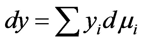
This is Gibb’s adsorption equation where y is the superficial adsorption density and μ is the chemical potential of the adsorbed species.
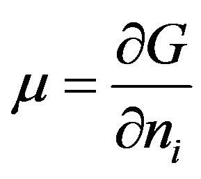
where G is Gibb’s free energy and ni is the amount of substance of the component or specie i.
Using Gibb’s adsorption equation as a basis, the variation of water oxide surface (interfacial) tension with ionic strength (I) maximum surface charge density (σmax), and pH has been developed from Gibbs adsorption equation. It is given as
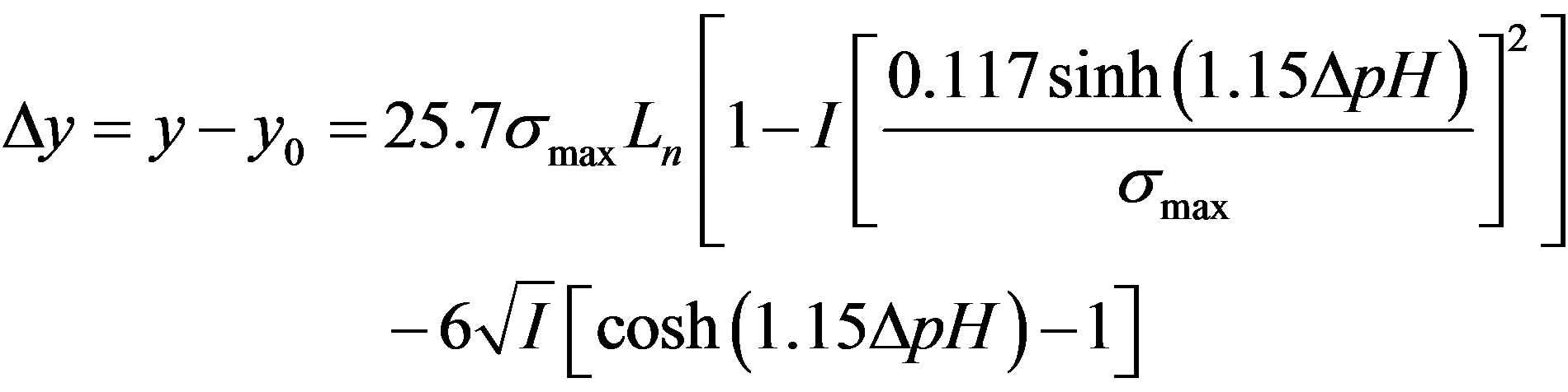
where y is given in  (interfacial tension) I is given in
  (ionic strength)
  is given in
  (max.surface charge) y0 means interfacial tension at equilibrium [52].
We assume that at equilibrium, all the chemical potentials of the different species in the solution are the same and the interfacial tension is zero (point of zero, interfacial tension (PZIT).
This assumption is correct if our system is compared with microemulsion systems which have very low (ultralow) surface tension at equilibrium [54].
The quantitative stable thermodynamic condition for the precipitation (growth) of metal ions in an alkaline medium is given as

pH above PZIT where secondary growth (Ostwald ripening) does not occur and the nanoparticles have definite stage is the stable state.
The size of the nanoparticles is directly related to the conditions for nucleation. These include pH, ionic strength and concentration of precursors [55].
Solid phases (particles, crystals thin films) evolve from solutions through nucleation and growth processes. The nucleation in this case occurs heterogeneously since the nuclei forms on an external object (glass slide).
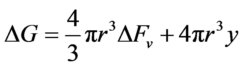
The total change in free energy of the system is given as
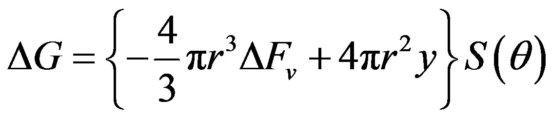
where 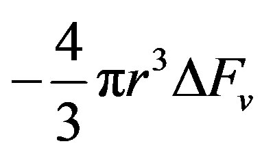 is the chemical component while
 is the surface component
  is the free energy per unit volume.
We assume that the new phase is spherical and therefore has a volume of  .
.
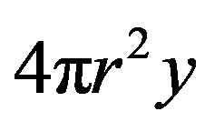
 is the surface component of the free energy due to surface tension
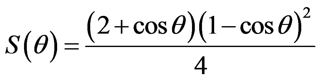
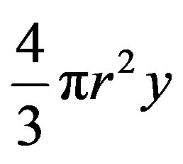
where θ is the wetting angle S(θ) differentiates the expression for change in free energy of the system from that of homogeneous nucleation.
Otherwise, they are basically the same.
Hence, for homogeneous nucleation,
 and the critical radius of the nucleus for nucleation to occur is obtained from the operation,
Or 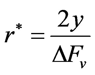
The free energy barrier for nucleation at r* (ΔG*) is obtained by substituting the value of r* in the expression for ΔG.
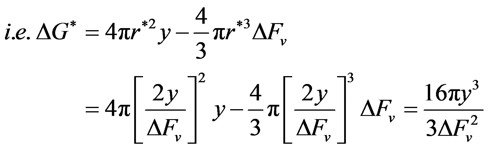
Hence, the barrier for nucleation at r* varies directly as the third power of the interfacial tension.
However, interfacial tension is dependent on pH, ionic strength and concentration of solution.
Thus ΔG* can be reduced by reducing the interfacial tension through the control of the pH, ionic strength or concentration of the solution [56-59].
This paper examines the effect of annealing temperature on the optical and solid state properties of the solid phase (thin film of cupric oxide) which evolved from a solution of 0.1 M Cu(NO3)2, 0.1 M C6H12N4 and 80 ml of H2O through heterogeneous nucleation and growth processes.
3. EXPERIMENTAL DETAILS
CuO thin films were deposited on clean glass substrates using Aqueous Chemical Growth Method.
The precursors used were equimolar (0.1 M) concentration of Cu(NO3)2 and C6H12N4 in 80 ml water.
We used a laboratory analytical microbalance to measure the masses of the chemicals while a measuring cylinder was used to determine the volume of water. All the component chemicals were put into a 100 ml pyrex bottle and were thoroughly mixed using a magnetic stirrer.
Labeled clean glass substrates were inserted in the pyrex bottle containing the chemicals after which the pyrex bottle was properly corked.
The pyrex bottle was then placed in an oven and the temperature of the oven was adjusted to 80˚C.
The pyrex bottle was left in the oven for an average of six hours for deposition to occur. After deposition, one of the samples (XB1) was left as-deposited while three (XB2, XB3 and XB4) were annealed at different temperature of 150˚C, 200˚C and 250˚C respectively.
We propose that the following chemical reactions resulted in the crystallization of CuO on the glass substrates.


Cu2+ was obtained from (Cu(NO3)2 in solution [60].
4. RESULTS AND DISCUSSION
We obtained the analysis of the elemental composition of sample XB1 using Rutherford Backscattering (RBS) spectroscopy. A 1.7 MV pelletron Tandem accelerator was used for this purpose.
This is shown in Figure 1.
Considering the elemental composition of sample XB1 shown in Table 1, it is established that the elements contained in sample XB1 are Cu (0.150%) and 0 (0.850%) while the glass substrate upon which the film was deposited consist of 0 (0.500%), Si (0.120%), Ca (0.100%), Al (0.100%) ad Na (0.180%). This is as contained in Figure 2.
The film thickness obtained is 720 nm.
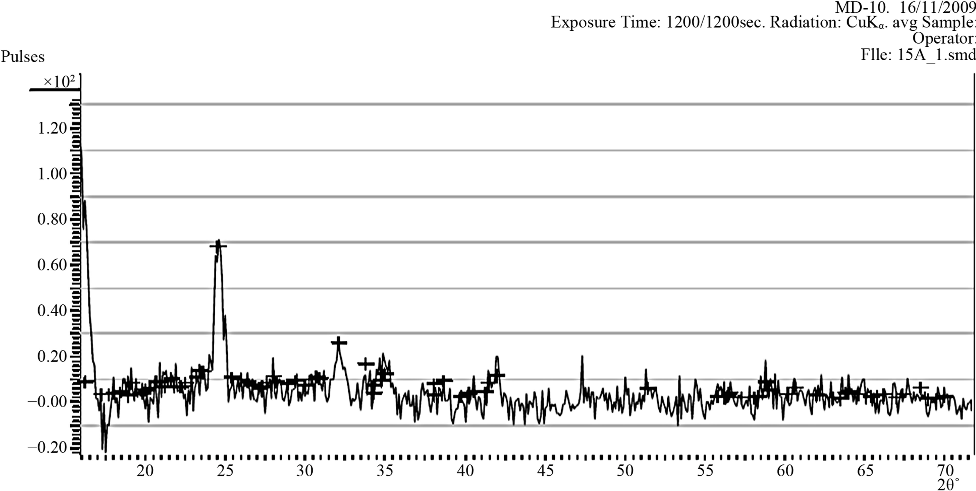
The CuO thin film samples (XB1 and XB2) were scanned continuously between 2θ = 0 and 2θ = 70˚ at step size of 0.03 and at time per step of 0.15 s using a diffractometer with a CuKα radiation source having a
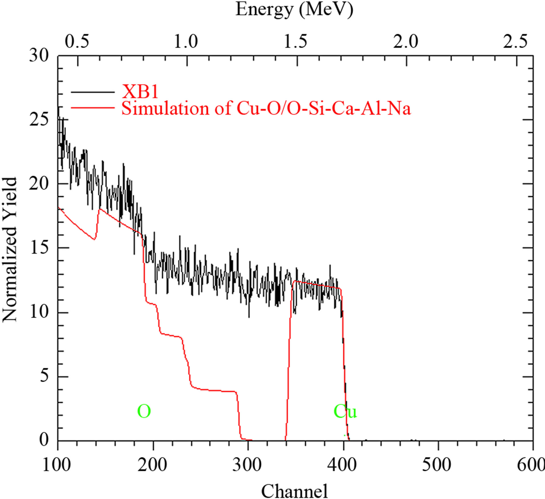
Figure 1. RBS analysis for ACG CuO thin film (sample XB1).
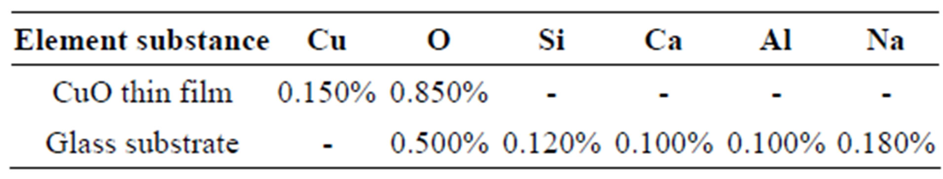
Table 1. Elemental composition of CuO thin film and substrate from RBS analysis.
 (a)
(a)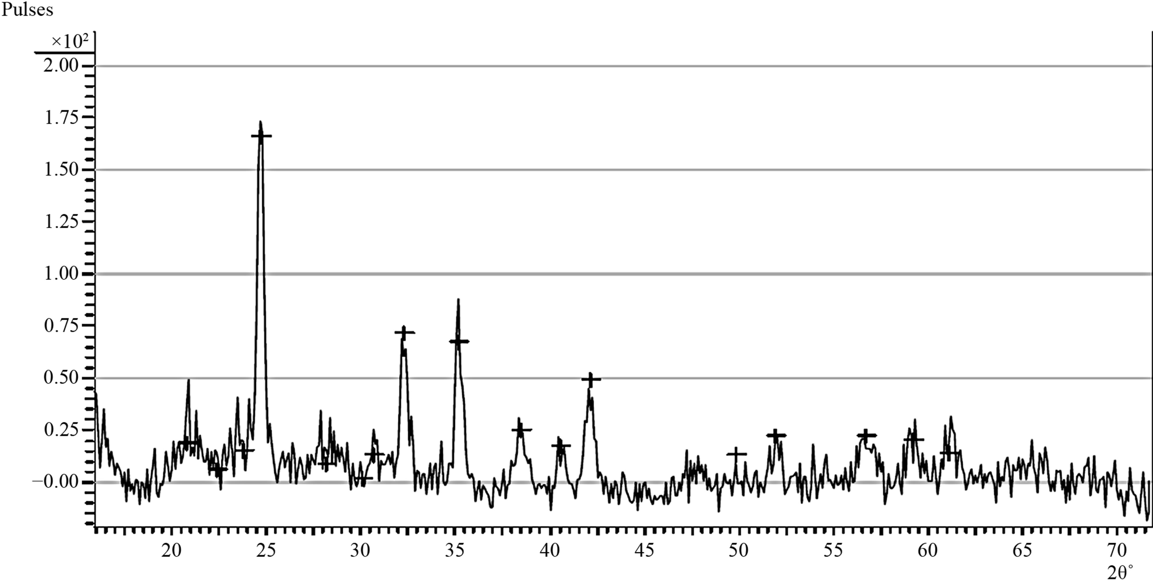 (b)
(b)
Figure 2. (a) Diffraction pattern of the as-prepared samples (XB1); (b) Diffraction pattern of the sample XB2 annealed XB2 at 150˚ for 2.5 hours.
wavelength of 1.54056 Å. This was done to enable us determine the crystalline nature of the thin film samples.
Figures 2(a) and (b) show the diffraction patterns of the as-deposited sample (XB1) and the sample annealed at 150˚C (XB2) for 2.5 hours.
As it is in Figure 2(a), all diffraction peaks can be indexed clearly to the monoclinic CuO phase having lattice constants a = 4.684 Å, b = 3.425 Å, c = 5.129 Å and β = 99.47˚ [61].
Figure 2(a) did not indicate the presence of impurities such as Cu2O or Cu(OH)2 as no other peaks except those of CuO are observed.
This suggests that the as-prepared sample is made purely of CuO molecules as confirmed from the RBS result.
However, this position does not rule out the possibility of the presence of small quantities of impurity molecules such as Cu(OH)2 which may have accumulated along grain boundaries of the crystallites that make up the film.
Figure 2(a) further indicate that reflections are strongest in the directions 2θ = 32.22˚ and 2θ = 35.13˚. These directions approximately correspond to the crystal planes having miller indices 110 and 111 respectively.
The diffraction patterns for CuO presented by F. Bayansal et al. (2011) [13], UnlingZou et al. (2011) [14] and A. Sagadevan et al. (2012) indicate that reflection is strongest along the 2θ = 35.13˚ and 2θ = 38.5˚ which correspond to the 110 and 111 planes respectively. Their diffraction patterns also indicate that reflection occurred in the 2θ = 32.22˚ direction but with a low intensity compared to the 2θ = 35.13˚ direction.
The difference in the planes along which the strongest reflections occur may be due to preparation method. Figure 2(b) indicates increase in intensities and decrease in widths of peaks resulting from annealing. This is indicative of high crystallinity. Thus, annealing improves the crystallinity of CuO thin films deposited using the Aqueous Chemical Growth Method. This is in agreement with the results of F. Bayansal et al. (2011) [13].
Figures 3-11 are the spectral analysis for the absorbance, transmittance, reflectance, absorption coefficient, direct band gap, extinction coefficient, real dielectric constant, imaginary dielectric constant and refractive index of the CuO ACG thin films investigated.
A Unico UV-2102 PC spectrophotometer was used for the spectral analysis.
Absorbance decreases with increasing annealing temperature.
The absorbance of all the samples decrease sharply from a common value of about 1.50 a.u at about 329.41 nm to about 0.81 a.u (XB1), 0.63 a.u (XB2), 0.52 a.u (XB3) and 0.45 a.u (XB4) at 400 nm.
Within the visible range, the absorbance value of some of the samples decrease from about 0.81 a.u to 0.75 a.u (XB1), 0.63 a.u to 0.62 a.u (XB2), 0.59 a.u to 0.52 a.u (XB3). However the absorbance of sample XB4 increases slowly from about 0.45 a.u to about 0.48 a.u within the visible range.
Between 700 nm and 900 nm, the absorbance values of the samples are fairly constant. While the value for samples XB1 and XB2 are about 0.75 a.u and 0.62 a.u within this range, the value for samples XB3 and XB4 are about 0.52 a.u and 0.45 a.u respectively.
Beyond 900 nm, absorbance value of all the samples decreases slowly with increasing wavelength.
Transmittance of the samples increases with increasing annealing temperature.
The transmittance of all the samples rises from a common value of about 3.16% at about 306 nm to peak values of about 35.67% (XB4), 26.32% (XB3), 22.90% Absorbance vs. wavelength
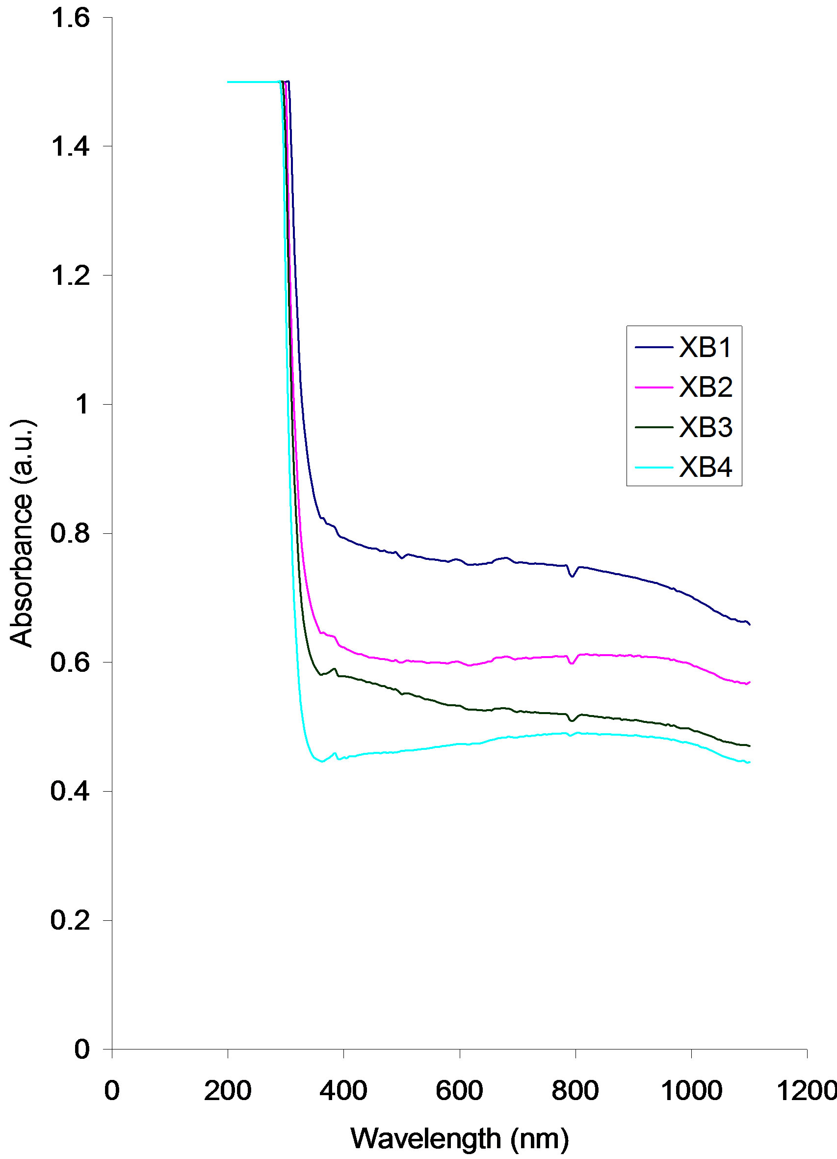
Figure 3. Absorbance vs. wavelength for ACG CuO thin films at different annealing temperatures.
Transmittance vs. wavelength
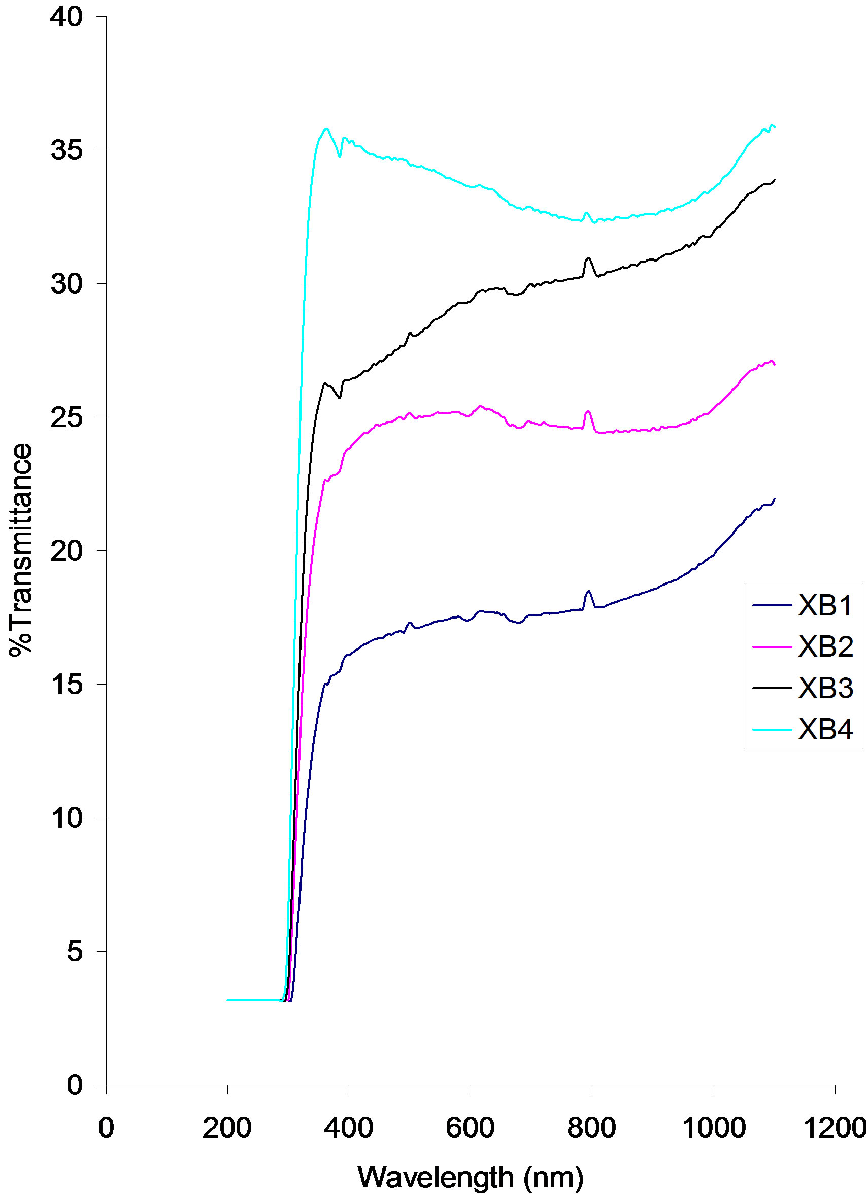
Figure 4. Transmittance vs. Wavelength for ACG CuO thin films at different annealing temperatures.
Reflectance vs. Wavelength
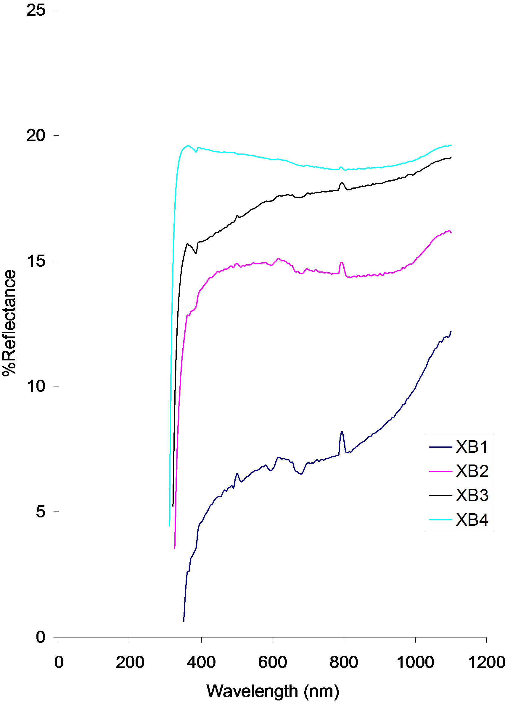
Figure 5. Reflectance vs. wavelength for ACG CuO thin films at different annealing temperature.
Absorption Coefficient
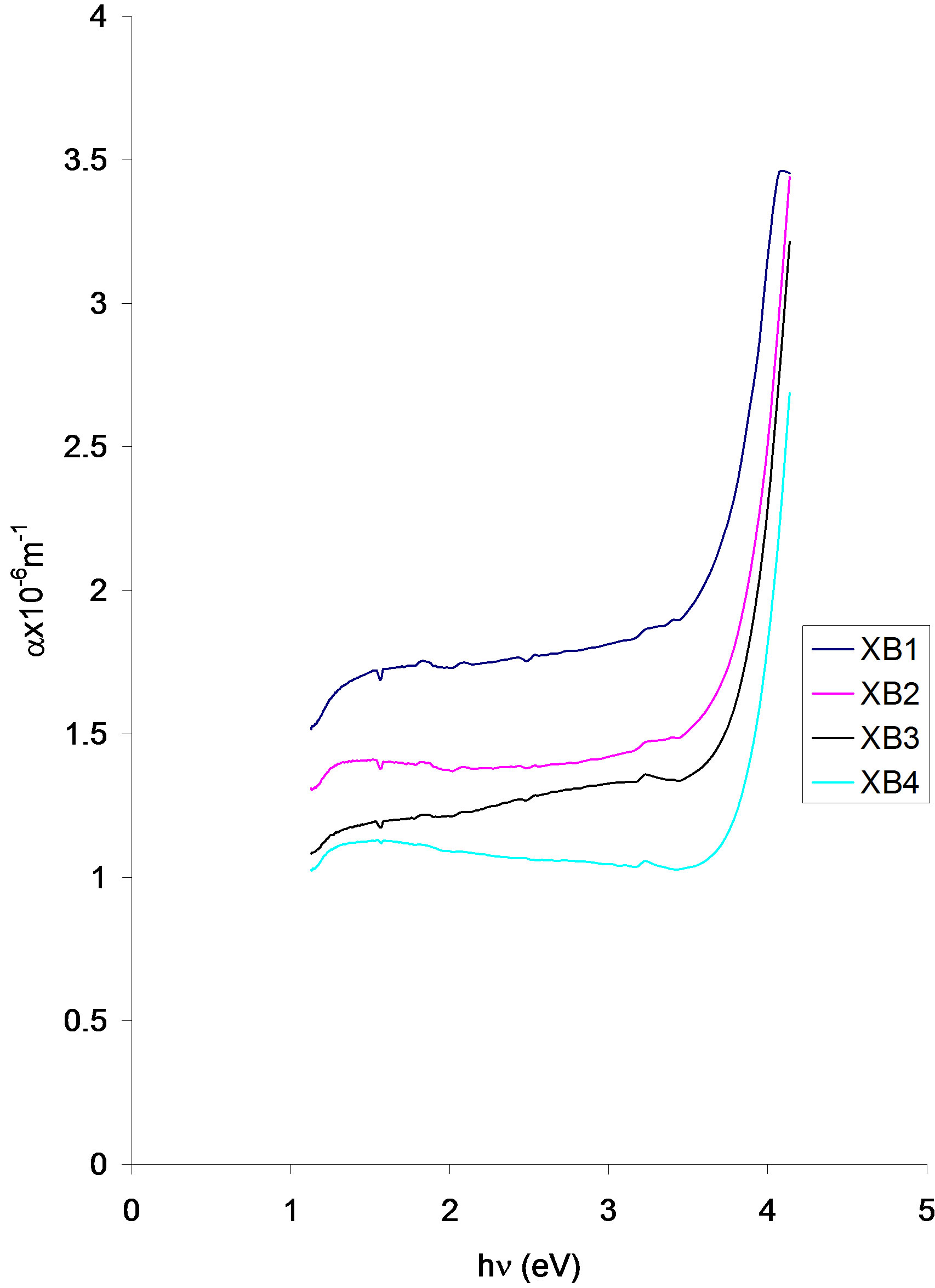
Figure 6. Absorption coefficient vs. photon energy for ACG CuO thin films at different annealing temperatures.
Direct band gap
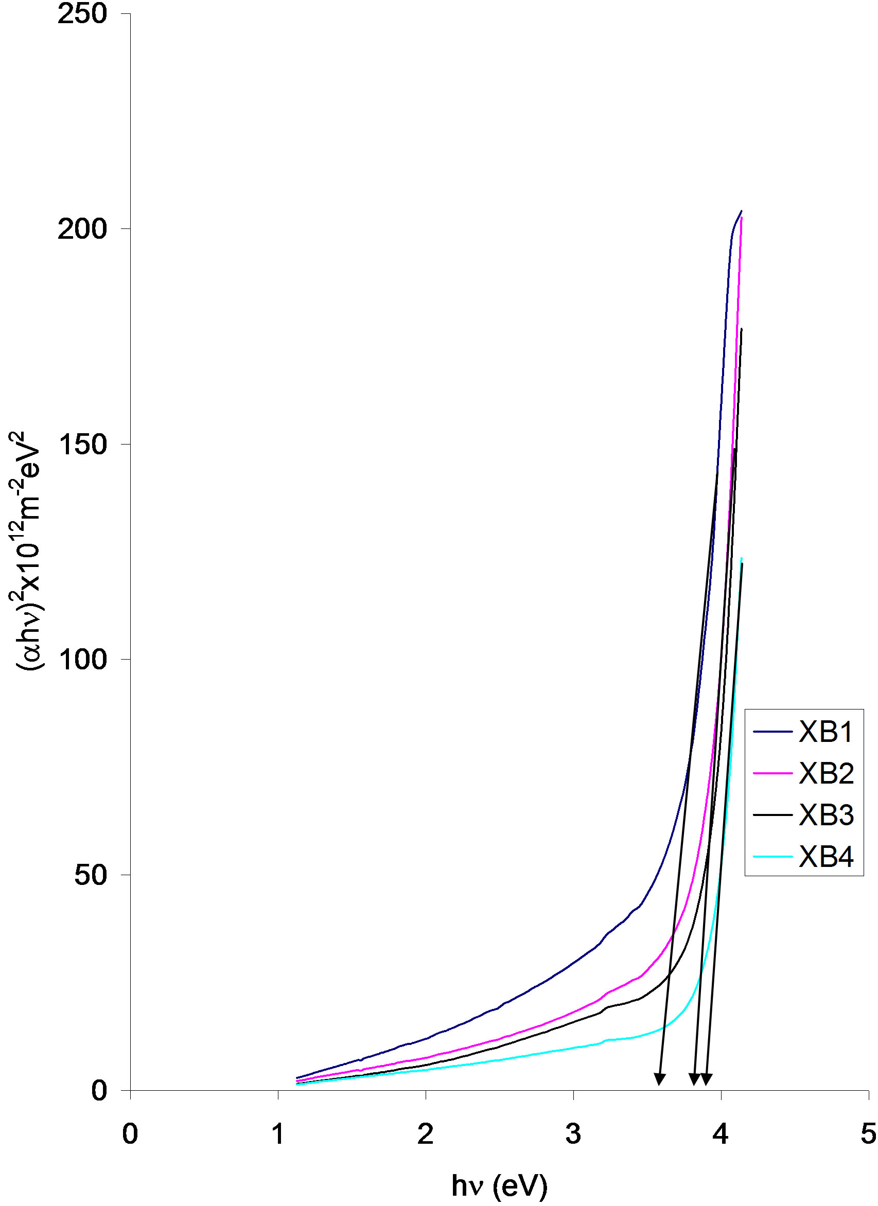
Figure 7. Direct band gap plot for ACG CuO thin films at different annealing temperature.
Extinction coefficient vs. photon energy
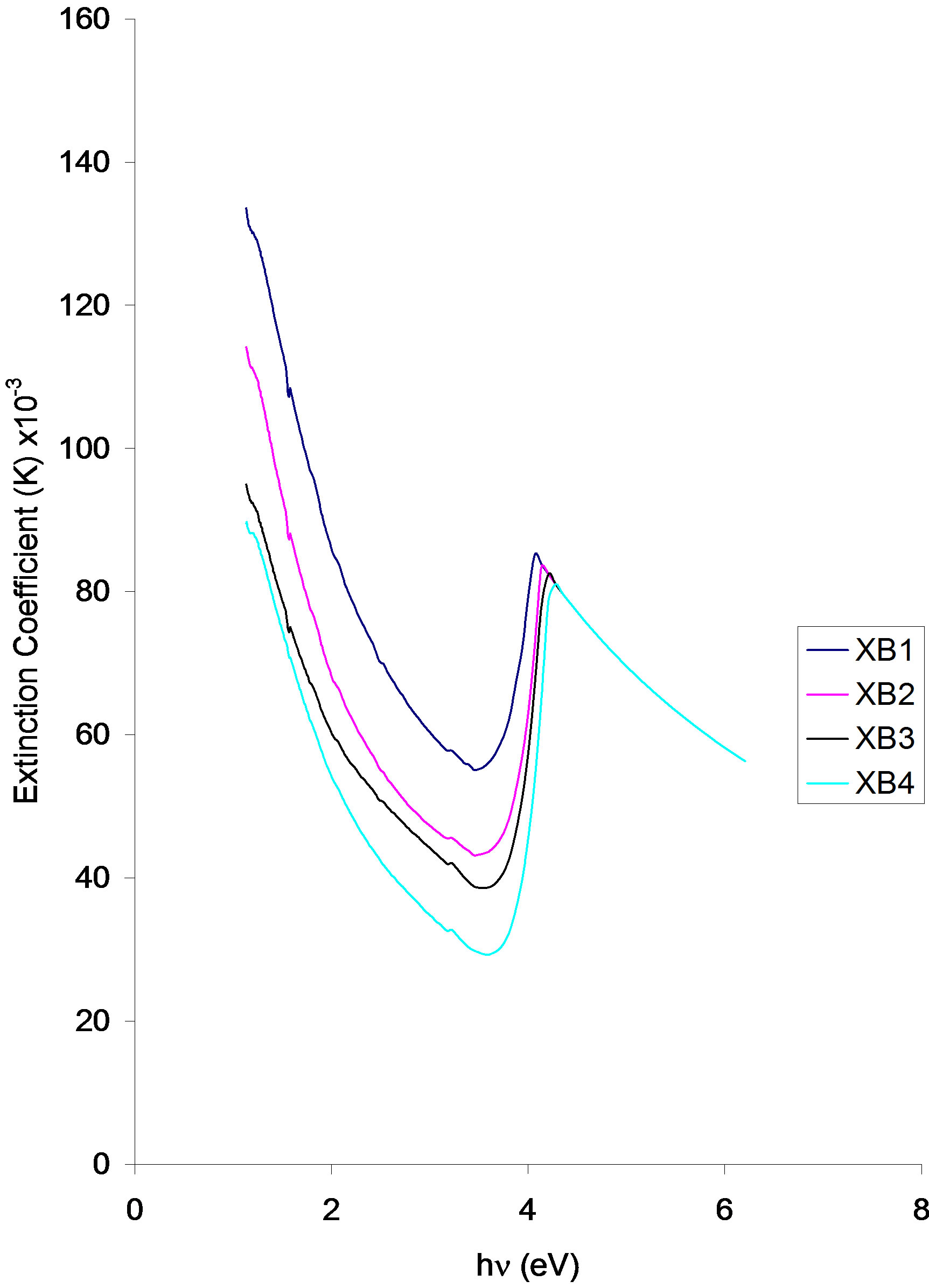
Figure 8. Extinction coefficient vs. photon energy for ACG CuO thin films at different annealing temperatures.
Real dielectric constant vs. photon energy
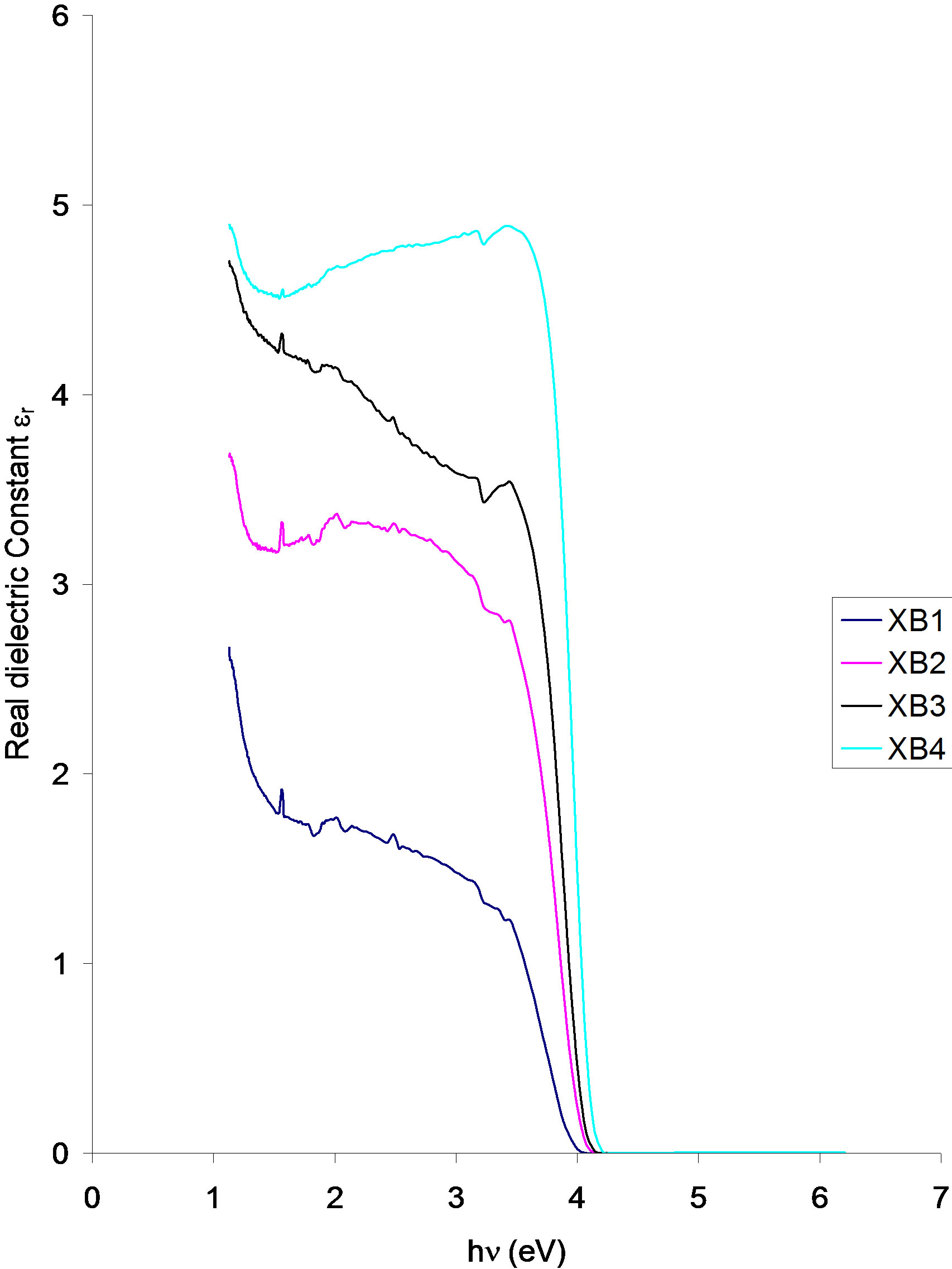
Figure 9. Real dielectric constant vs. Photon energy for ACG CuO thin films at different annealing temperatures.
Imaginary dielectric constant vs. photon energy
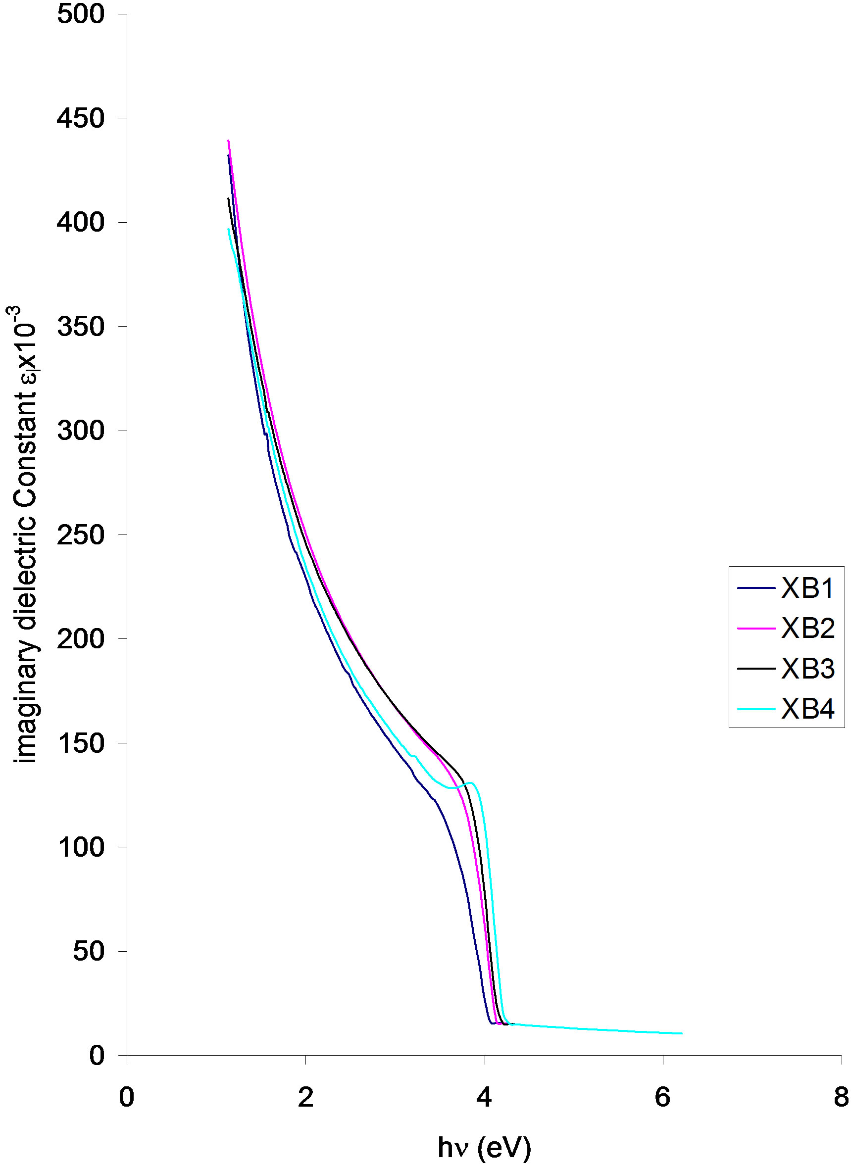
Figure 10. Imaginary dielectric constant vs. photon energy for ACG CuO thin film at different annealing temperatures.
Reflective index vs. photon energy
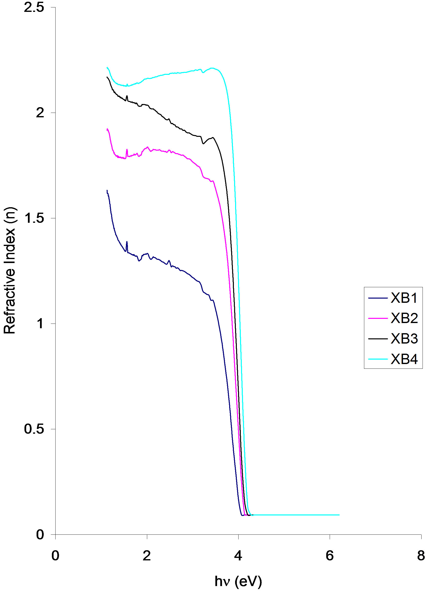
Figure 11. Refractive index vs. photon energy for ACG CuO thin films at different annealing temperatures.
(XB2) ad 15.53% (XB1) in the infra-red region.
A small decrease in transmittance occurs around 400 nm in all the samples. Between 400 nm and 700 nm, the transmittance of samples XB1, XB2 and XB3 rise from 15.53% to 17.50%, 22.90% to 25.00% and 26.32% to 29.61% respectively while the transmittance of sample XB4 decreases from 35.00% to about 33.29%.
Above 700 nm the transmittance of samples XB1, XB2 and XB3 increases while that of sample XB4 follows a parabolic path.
Reflectance of the samples increases with increasing annealing temperature. The reflectance of the as-prepared sample (XB1) rises from about 0.67% at about 347.06 nm to 4.5% at 400 nm while the reflectance of samples XB2, XB3 and XB4 rise sharply from 3.58%, 5.17% and 7.00% at 329.41 nm, 323.53 nm and 317.65 nm respectively to about 13.50%, 15.75 and 19.50% respectively at 400 nm.
Within the visible region, the reflectance of the XB4 sample decreases slowly to 19.08% while the reflectance of samples XB3, XB2 and XB1 increases to 17.33%, 14.75% and 7.00% respectively in the direction of increasing wavelength.
In the infra-red region, reflectance increases in the direction of increasing wavelength.
Absorption coefficient decreases with increasing annealing temperature. The absorption coefficient of three samples increased from 1.58 × 10⁻⁶ (XB1), 1.29 × 10⁻⁶ (XB2) and 1.08 × 10⁻⁶ (XB3) at about 1.14 eV in the infra-red region to about 1.93 × 10⁻⁶ (XB2), 1.58 × 10⁻⁶ (XB2) and 1.29 × 10⁻⁶ (XB3) at about 3.62 eV in the visible region.
The absorption coefficient of sample XB4 increases in the direction of increasing photon energy in the infra-red region and thereafter decreased slowly until it attained the value of about 1.03 × 10⁻⁶ at 3.62 eV.
Between 3.62 eV and 400 eV, the absorption coefficient of the samples rises sharply and attained different peak values which decreases with increasing annealing temperature.
There is an increasing blue shift with increasing annealing temperature. The direct band gap of the as-prepared sample (XB1) is about 3.55, while that of the XB2 and XB3 samples is about 3.80. The XB4 sample has a direct band gap of about 3.85.
Aiping Chen et al. (2009) [61] estimated the direct band gap of CuO thin films deposited on Si (100) substrates using pulsed laser deposition technique to be 2.12 eV.
By comparison, our values are higher. These relatively high values of direct band gap for CuO thin films are attributable to preparation method. Several researchers have reported that the band gap of CuO can be changed to a wide range depending on the preparation conditions of CuO [62-67].
The high values of direct band gap obtained for ACG CuO thin films make them highly suitable for use as window layer in solar cells.
The Extinction coefficient of the samples decreases with increasing annealing temperature.
The extinction coefficient of the samples decreases parabolically from 133.89 × 10⁻³ (XB1), 11.89 × 10⁻³ (XB2), 93.89 × 10⁻³ (XB3) and 89.44 × 10⁻³ (XB4) at about 1.15 eV in the infra-red region to about 81.11 × 10⁻³ (XB1), 82.22 × 10⁻³ (XB2), 83.33 × 10⁻³ (XB3) and 84.44 × 10⁻³ (XB4) at 4.0 eV (XB1), 4.08 eV (XB2), 4.15 eV (XB3) and 4.23 eV (XB4) respectively.
The minimum values of the extinction coefficient of the samples are 57.78 × 10⁻³ (XB2) and 29.44 × 10⁻³ (XB1) and they all occurred at about 3.54 eV.
The extinction coefficient values of the samples at 2.0ev are approximately 94.44 × 10⁻³ (XB1), 72.78 × 10⁻³ (XB2), 64.44 × 10⁻³ (XB3) and 59.44 × 10⁻³ (XB4).
The real dielectric constant of the samples increases with increasing annealing temperature. The real dielectric constant of the samples decreases parabolically from about 4.92 (XB4), 4.73 (XB3), 3.67 (XB2) and 2.65 (XB1) at about 1.16 eV in the infra-red region to about 4.73 (XB4), 4.16 (XB3), 3.35 (XB2) and 1.82 (XB2) respectively at 2.0 eV.
In the visible region, the real dielectric constant of the XB4 sample increased slowly from 4.73 at 2.0 eV in the direction of increasing photon energy to about 4.92 at 4.0 eV. However, the dielectric constant of the other samples decreases from 4.16 (XB3), 3.35 (XB2) and 1.82 (XB1) in the direction of increasing photon energy to about 3.69 (XB3), 2.84 (XB2) and 1.26 (XB1) at about 3.5 eV in the visible region.
Beyond 3.5 eV and in the direction of increasing photon energy, the real dielectric constant of all the samples decreases sharply to 0. This occurs at about 4.13 eV (XB4), 406 eV (XB3 and XB2) and 4.0 eV (XB1).
The imaginary dielectric constant of the samples increases with increasing annealing temperature. The imaginary dielectric constant of the samples decreases parabolically from approximately 39.67 × 10⁻³ (XB4), 410.00 × 10⁻³ (XB3), 433.33 × 10⁻³ (XB2) and 440 × 10−3 (XB1) at about 1.04 eV in the infra-red region to 130.00 × 10⁻³ at about 4.0 eV (XB4), 3.38 eV (XB3), 3.85 eV (XB2) and 3.77 eV (XB1).
The values of the imaginary dielectric constant of the samples at 2.0 eV are about 243.33 × 10⁻³ (XB1), 250 (XB4) and 263.33 × 10⁻³ (XB2 and XB3).
The imaginary dielectric constant for all the samples decreases sharply from about 130.00 × 10⁻³ to about 15 × 10−3 at 4.0 eV (XB1), 4.08 eV (XB2, XB3 and 4.15 eV (XB4).
Refractive index of the samples increases as annealed temperature increases. All the samples have their peak refractive index at 1.15eV in the infra-red region. The values are 1.63 (XB1), 1.93 (XB2), 2.17 (XB3) and 2.20 (XB4).
The refractive indices for all the samples however followed a parabolic path with increasing photon energy within the infra-red region. A small peak in the refractive index occurred at 2.0 eV for all the samples. The values are 1.33 (XB1), 1.83 (XB2), 2.03 (XB3) and 2.17 (XB4). Except for sample XB4 in which its refractive index increases slowly with increase in photon energy up to 3.54 eV, the refractive index of each of the samples decreases with increase in photon energy from 2.0 eV up to 3.54 eV.
From 3.54 eV, the refractive index of each of the samples decreases sharply to about 0.08 in the direction of increasing photon energy up to 4.0 eV (XB1), 4.08 eV (XB2) and (XB3) and 4.15 eV (XB4).
5. CONCLUSIONS
We have successfully deposited thin films of CuO having average thickness of 720nm on clean glass substrates and have also determined the effect of annealing temperature on their optical and solid state properties.
Our findings indicate that while absorbance and absorption/extinction coefficients of the deposited films decreases with increasing annealing temperature, the transmittance, reflectance, direct band gap, real/imaginary dielectric constants and refractive index of the films increases with increasing annealing temperature. Also, there is an improvement in the crystallinity of deposited films as annealing temperature increases.
The high direct band gap of the as-deposited ACG CuO thin films and those annealed at different temperatures indicate their suitability for use as window layer in solar cells among other opto-electronic applications.
REFERENCES
- Li, J., Vizkelethy, G., Revesz, P., Mayer, J.W. and Tu, K.N. (1991) Oxidation and reduction of copper oxide thin films. Journal of Applied Physics, 69, 1020. doi:10.1063/1.347417
- Ohya, Y., Ito, S., Ban, T. and Takahashi, Y. (2000) Preparation of CuO thin films and their electrical conductivity. Eng. Mater, 181, 113-116.
- Balamurugan, B. and Mehta, B.R. (2001) Optical and structural properties of nanocrystalline copper oxide thin films prepared by activated reactive evaporation. Thin Solid Films, 396, 90-96. doi:10.1016/S0040-6090(01)01216-0
- Tang, F., Yao, W.Y., Zhang, Y.F., Ma, Y.T., Teng, Y., Xu, T.G., Lang, S.H. and Zhu, Y.F. (2008) Synthesis of flowerlike CuO nanostructures as a sensitive sensor for catalysis. Sensors and Actuators, B134, 761-768.
- Jeong, Y.K. and Choi, G.M. (1996) Nanostoichiometry and electrical conduction of CuO. Journal of Physics and Chemistry of Solids, 57, 81-84. doi:10.1016/0022-3697(95)00130-1
- Herrain, J., Mandayo, G.G. and Castan, E. (2007) Physical behavior of BaTiO3-CuO thin film under carbon dioxide atmosphere. Sensors and Actuators B: Chemical, 127, 370-375. doi:10.1016/j.snb.2007.04.035
- Marabelli, F., Parrsavinciny, G.B. and Driolli, F.S. (1995) Optical gap of CuO. Physical Review B, 52, 1433-1436. doi:10.1103/PhysRevB.52.1433
- Yang, B.X., Thurston, T.R., Tranquada, J.M. and Shirane, G. (1989) Magnetic neutron scattering study of single crystal cupric oxide. Physical Review B, 39, 4343-4349
- Forsyth, J.B., Brown, P.J. and Wanklyn, B.M. (1988) Magnetism in cupric oxide. Journal of Physics C: Solid State Physics, 21, 2917-2929. doi:10.1088/0022-3719/21/15/023
- Ota, S.B. and Gmelin, E. (1992) Incommensurate antiferromagnetism in copper(II) oxide: Specific-heat study in a magnetic field. Physical Review B, 46, 11632-11635. doi:10.1103/PhysRevB.46.11632
- Qin, H.W., Zhang, Z.L., Liu, X., Zhang, Y.J. and Hu, J.F. (2010) Room-temperature ferromagnetism in CuO sol-gel powders and films. Journal of Magnetism and Magnetic Materials, 322, 1994-1998. doi:10.1016/j.jmmm.2010.01.021
- Eliseev, A.A., Lukashin, A.V., Vertegel, A.A., Heifets, L.I., Zhirov, A.I. and Tretyakov, Y.D. (2000) Complexes of Cu(II) with polyvinyl alcohol as precursors for the preparation of CuO/SiO2 nanocomposites. Material Research Innovations, 3, 308-312. doi:10.1007/PL00010877
- Bayansal, F., Kahraman, S., Cankaya, G., Cetinkara, H.A. Guider, H.S. and Cakaya, H.M. (2011) Growth of homogeneous CuO nano-structured thin films by a simple solution method. Journal of Alloys and Compounds, 509, 2094- 2098. doi:10.1016/j.jallcom.2010.10.146
- Zou, Y.L., Li, Y., Zhang, N. and Liu, X.L. (2011) Flowerlike CuO Synthesized by CTAB-assisted hydrothermal method. Bulletin of Materials Science, 34, 976-971.
- Liu, B. and Zeng, H.C. (2004) Mesoscale organization of CuO nanoribbons: Formation of “dandelions”. Journal of the American Chemical Society, 126, 8124-8125. doi:10.1021/ja048195o
- Gao, P., Chen, Y.J., Lv, H.J., Li, H.L. and Gao, H.J. (2009) Synthesis of CuO nanoribbon arrays with noticeable electrochemical hydrogen storage ability by a simple precursor dehydration route at lower temperature. International Journal of Hydrogen Energy, 34, 3065-3069. doi:10.1016/j.ijhydene.2008.12.050
- Su, Y.K., Shen, C.M., Yang, H.T., Li, H.L. and Gao, H.J. (2007) Controlled synthesis of highly ordered CuO nanowire arrays by template-based sol-gel route. Transactions of Nonferrous Metals Society of China, 17, 783-786. doi:10.1016/S1003-6326(07)60174-5
- Zheng, L.K. and Liu, X.J. (2007) Solution-phase synthesis of CuO hierarchical nanosheet at near-neutral pH and near room-temperature. Materials Letters, 61, 2222-2226. doi:10.1016/j.matlet.2006.08.063
- Zarate, R.A., Hevia, F., Fuentes, S., Fuenzalida, V.M. and Zuniga, A. (2007) Novel route to synthesize CuO nanoplatelets. Journal of Solid State Chemistry, 180, 1464- 1469. doi:10.1016/j.jssc.2007.01.040
- Dar, M.A., Kim, W.B., Sohn, J.M. and Shin, H.S. (2008) Structural and magnetic properties of CuO nanoneedles synthesized by hydrothermal method. Applied Surface Science, 254, 7477-7481.
- Morales, J., Sánchez, L., Martín, F., Ramos-Barrado, J.R. and Sánchez, M. (2004) Nanostructured CuO thin film electrodes prepared by spray pyrolysis: A simple method for enhancing electrochemical performance of CuO in lithium cells. Electrochemical Acta, 49, 4589-4597. doi:10.1016/j.electacta.2004.05.012
- Poizor, P., Laruella, S., Dupont, L. and Tarascon, J.M. (2000) Nano-sized transition metal oxides as negative electrode materials for lithium-ion batteries. Nature, 407, 496-499. doi:10.1038/35035045
- Awgouropoules, G., Joaminides, T., Papadopoulou, C., Batista, J, Hocever, S. and Matralis, H.K. (2002) A comparative study of Pt/γ-Al2O3, Au/α-Fe2O3 and CuO-CeO2 catalyst for the selective oxidation of carbon monoxide in excess hydrogen. Catalysis Today, 75, 157-167. doi:10.1016/S0920-5861(02)00058-5
- Nagase, K., Zhang, Y., Kodama, Y. and Kakuta, J. (1999) Dynamic study of the oxidation state of copper in the course of carbon monoxide oxidation over powdered CuO and Cu2O. Journal of Catalysis, 187, 123-130. doi:10.1006/jcat.1999.2611
- Chen, J. Huang, N.Y., Deng, S.Z., She, J.C., Xu, N.S., Zhang, W.X., Wen, X.G. and Yang, S.H. (2005) Effects of light illumination on field emission from CuO nanobelt arrays. Applied Physics Letters, 86, 157-159.
- Liao, L., Zhang, Z., Yan, B., Zheng, Z., Bao, Q.L., Wu, T., Li, C.M., Shen, Z.X., Zhang, J.X., Gong, H., Li, J.C. and Yu, T. (2009) Multifunctional CuO nanowires devices: p-type field effect transistors and selective CO gas sensors. Nanotechnology, 20, 085203. doi:10.1088/0957-4484/20/8/085203
- Frietsh, M., Zudock, F., Goschnick, J. and Bruns, M. (2000) CuO catalytic membrane asselectivity trimmer for metal oxide gas sensors. Sensors and Actuators B: Chemical, 65, 379-381. doi:10.1016/S0925-4005(99)00353-6
- Chowdhuri, A., Gupta, V., Streenvas, K., Kumar, R., Mozundar, S. and Patanjali, P.K. (2004) Response speed of SnO2-based H2S gas sensors with CuO nanoparticals. Applied Physics Letters, 84, 1180-1182. doi:10.1063/1.1646760
- Vasiliev, R.B., Rumyanteva, M.N., Yakovlev, N.V. and Gaskor, A.M. (1998) CuO/SnO2 thin film heterostructures as chemical sensors to H2S. Sensors and Actuators B: Chemical, 50, 186-193. doi:10.1016/S0925-4005(98)00235-4
- Nakamura, Y., Zhuang, H., Kishimoto, A., Okada, O. and Yanagida, H. (1998) Enhanced CO and CO2 gas sensitivity of the CuO/ZnO heterocontact made by quenched CuO ceramics. Journal of the Electrochemical Society, 145, 632-637. doi:10.1149/1.1838315
- Liu, Y.L., Liao, L., Li, J.C. and Pan, C.X. (2007) From Copper nanocrystalline to CuOnanoneedle array: Synthesis, growth mechanism and properties. Journal of Physical Chemistry C, 111, 5050-5056. doi:10.1021/jp069043d
- Ray, S.C. (2001) Preparation of copper oxide thin film by the sol-gel-like dip technique and study of their structural and optical properties. Solar Energy Materials and Solar Cells, 68, 307-312.
- Maruyama, T. (1998) Copper oxide thin films prepared by chemical vapor deposition from copper dipivaloylmethanate. Solar Energy Materials and Solar Cells, 56, 85-92.
- Yoon, K.H., Choi, W.I. and Kang, D.H. (2000) Photoelectrochemical properties of copper oxide thin films coated on an n-Si substrate. Thin Solid Films, 372, 250- 256. doi:10.1016/S0040-6090(00)01058-0
- Rakhshani, A.E. (1986) Preparation, characteristics and photovoltaic properties of cuprous oxide—A review. Solid-State Electron, 29, 7-17.
- Dai, P.C., Mook, H.A., Aeppli, G., Hayden, S.M. and Dogan, F. (2000) Resonance as a measure of pairing correlations in the high-Tc superconductor YBa2Cu3O6.6. Nature, 406, 965-968. doi:10.1038/35023094
- Eskes, H., Tjeng, L.H. and Sawatzky, G.A. (1990) Cluster mode calculation of the electronic structure of CuO. Physical Review B, 41, 288-292. doi:10.1103/PhysRevB.41.288
- Patake, V.D., Joshi, S.S., Likhande, C.D. and Joo, O.-S. (2009) Electrode posited porous and amorphous Copper oxide film for application in super capacitor. Materials Chemistry and Physics, 114, 6-9. doi:10.1016/j.matchemphys.2008.09.031
- Muller, K.H. (2001) High-Tc supperconductors and related materials. Kluwer Academic, Dordrecht.
- Brookshier, M.A., Chusuei, C.C. and Goodman, D.W. (1999) Control of CuO particle size on SiO2 by spin coating. Langmuir, 15, 2043-2046. doi:10.1021/la981325k
- Bae, H.Y. and Choi, G.M. (1999) Electrical and reducing gas sensing properties of ZnO and ZnO-CuO thin films fabricated. Sensors and Actuators B: Chemical, 55, 47-54. doi:10.1016/S0925-4005(99)00038-6
- Xu, J.F., Ji, W., Shen, Z.X., Tang, S.H., Ye, X.R., Jia, D.Z. and Xin, X.Q. (1999) Preparation of CuO and characterization nanocrystals. Journal of Solid State Chemistry, 147, 516-519. doi:10.1006/jssc.1999.8409
- Su, Y.K., Shen, C.M., Yang, H.T., Li, L. and Gao, H.J. (2007) Controlled synthesis of highly ordered CuO nanowire arrays by template based sol-gel route. Transactions of Nonferrous Metals Society of China, 17, 783-786. doi:10.1016/S1003-6326(07)60174-5
- Tang, X.L., Ren, L., Sun, L.N., Tian, W.G., Cao, M.H. and Hu, C.W. (2006) A solvothermal route to Cu2O nanocubes and Cu nanoparticles. Chemical Research in Chinese Universities, 22, 547-551. doi:10.1016/S1005-9040(06)60159-1
- Song, X., Yu, H. and Sun, S. (2005) Single Crystalline CuOnanobelts fabricated, by aconvenient route. Journal of Colloid and Interface Science, 289, 588-591.
- Yuan, C.O., Jiang, H.F., Lin, C. and Liao, S.J. (2007) Shape and size-controlled electrochemical synthesis of cupric oxide nanocrystals. Journal of Crystal Growth, 303, 400-406. doi:10.1016/j.jcrysgro.2006.12.047
- Chen, J.T., Zhang, F., Wang, J., Zhang, G.A., Mian, B.B., Fan, X.Y., Yan, D. and Yan, P.X. (2008) CuO nanowires synthesized by thermal oxidation route. Journal of Alloys and Compounds, 454, 268-273.
- Vayssieres, L. (2004) On the design of advanced metal oxide nanomaterials. International Journal of Nanotechnology, 1, 1-41.
- Hu, X., Masuda, Y., Olyi T. and Kato, K. (2009) Fabrication of ZnO nanowhiskers array film by forced-hydrolysisinitiated-nucleation technique using various templates. Thin Solid Films, 518, 621-624.
- Zhang, X., Wang, L. and Zhow, G. (2005) Synthesis of well-aligned ZnO nanowires with catalysts. Reviews on Advanced Materials Science, 10, 69-72.
- Mammah, S.L., Opara, F.E., Sigalo, F.B., Ezugwu, S.C. and Ezema, F.I. (2012) Effect of concentration on the optical and solid state properties of ZnO thin films deposited by Aqueous Chemical Growth (ACG) method. Journal of Modern Physics, 3, 947-954. doi:10.4236/jmp.2012.39124
- Vayssières, L., Chanéac, C., Tronc, E. and Jolivet, J.P. (1998) size tailoring of magnetite particles formed by aqueous precipitation: An example of thermodynamic stability of nanometric oxide particles. Journal of Colloid and Interface Science, 205, 205-212. doi:10.1006/jcis.1998.5614
- Vayssieres, L. (1995) Précipitation de Nanoparticilues d'- oxydes en solution Aqueuse: Controleôle de la croissance et de la tension interfaciale. Ph.D. Thesis, Universite Pierre et Marie Curie, Paris, 1-145.
- Aveyard, R. (1987) Ultralow tensions and microemulsions. Chemistry & Industry, 14, 474-478.
- Edelstein, H., Rahman, Z. and Schubert, U. (2002) Nanostructured material. Springer-Verlage, Berlin.
- Mendez-Villuendas, E. and Bowles, R.K. (2007) Surface nucleation in the freezing of gold nanoparticles. Physical Review Letters, 498, 159901.
- Abraham, F.F. (1974) Homogeneous nucleation: Theory. Academy Press, New York.
- Anisimov, M.P. (2003) Nucleation: Theory and experiment. Russian Chemical Reviews, 72, 591-600. doi:10.1070/RC2003v072n07ABEH000761
- Schmelzer, J. (Ed), Fokin, Yuritsyn, Zanotto (2005) Nucleation theory and application, nucleation and crystallization kinetics in silicate glasses: Theory and experiment. Wiley-VCH, Verlag, GmbH and Co., Berlin, 76-83.
- Lee, S.F., Lee, L.Y. and Change, Y.P. (2009) A nanostructural zinc oxide electrode prepared by a hydrothermal method. Journal of Science and Engineering Technology, 5, 13-20.
- Cheng, A.P., Yang, G., Long, H., Li, F., Li, Y.H. and Lu P.X. (2009) Non linear optical properties of laser deposited CuO thin films. Thin Solid Films, 517, 4277-4280.
- Serin, T., Yildiz, A., Sahin, S.H. and Serin, N. (2001) Extraction of important electrical parameters of CuO. Physics B, 408, 575-578.
- Alkoy, E.M. and Kelly, P. (2000) The structure and properties of copper oxide and copper aluminium oxide coatings prepared by pulsed magnetron sputtering of powder targets. Vacuum, 79, 221-230. doi:10.1016/j.vacuum.2005.03.011
- Ray, S.C. (2001) Preparation of copper oxide thin film by the sol-gel-like dip technique and study of their structural and optical properties. Solar Energy Materials and Solar Cells, 68, 307-312. doi:10.1016/S0927-0248(00)00364-0
- Pierson, J.F., Thobor-Keck, A. and Billiard A. (2003) Cuprite, paramelaconite and tenorite films deposited by reactive magnetron sputtering. Applied Surface Science, 210, 359-367. doi:10.1016/S0169-4332(03)00108-9
- Nair, M., Guerrero, L., Arenas, O.L. and Nair, P.K. (1999) Chemically deposited copper oxide thin films: Structural, optical and electrical characteristics. Applied Surface Science, 150, 143-153. doi:10.1016/S0169-4332(99)00239-1
- Seto, J.Y.W. (1975) The electrical properties of polycrystalline silicon thin films. Journal of Applied Physics, 46, 5247-5254. doi:10.1063/1.321593