Materials Sciences and Applications
Vol. 4 No. 4 (2013) , Article ID: 30659 , 6 pages DOI:10.4236/msa.2013.44034
Enhancement of Performance of Organic Light Emitting Diodes by Using Tiand Mo-Oxide Nano Hybrid Layers
![]()
1University of Engineering and Technology, Vietnam National University Hanoi, Hanoi, Vietnam; 2Water Resources University, Hanoi, Vietnam; 3Institute of Materials Science, Vietnamese Academy of Science and Technology, Hanoi, Vietnam; 4Department of Physics, Concordia University, Montreal, Canada.
Email: dinhnn@vnu.edu.vn
Copyright © 2013 Nguyen Nang Dinh et al. This is an open access article distributed under the Creative Commons Attribution License, which permits unrestricted use, distribution, and reproduction in any medium, provided the original work is properly cited.
Received November 21st, 2012; revised December 12th, 2012; accepted January 14th, 2013
Keywords: Organic Light Emitting Diodes (OLED); Hybrid Heterojunctions; Curent-Voltage (I-V) Characteristic; Luminous Efficiency
ABSTRACT
Nanorod-like TiO2 (nc-TiO2) and MoO3 (nc-MoO3) films were thermally grown from Tiand Mo-metallic wafers. Nanohybrid films of N,N’-diphenyl-N,N’-bis(1-naphthyl)(1,1’-biphenyl)-4,4’diamine (NPB)/TiO2 and NPB/MoO3 used as anode/hole transport layer (HTL) heterojunctions in blue organic light emission diodes (OLEDs) were prepared by coating NPB onto the nc-TiO2 and nc-MoO3 and TiO2. Characterization of the nanostructured hybrid layers showed that both the photoluminescent property and current-voltage (I-V) characteristics of the hybrid materials were significantly enhanced in comparison with the standard NPB polymer. The electroluminous efficiency of the hybrid devices was considerably enhanced in comparison with the standard device. This suggests a useful application for fabricating “reverse” OLEDs, where the emission light goes-out through the semitransparent cathode, instead of the indium tin oxide (ITO) anode. For this, the ohmic contacts of conducting wires to metallic electrodes can be made much better than to ITO anodes.
1. Introduction
Recently, there has an been increasing interest in both theoretical and experimental works on conducting polymers and polymer-based devices, due to their potential application in optoelectronics, organic light emitting diode (OLED) displays, solar flexible cells, etc. [1-4]. Similar to inorganic semiconductors, from the viewpoint of energy bandgap, semiconducting polymers also have a bandgap—the gap between the highest occupied molecular orbital (HOMO) and the lowest unoccupied molecular orbital (LUMO). When sufficient energy is applied to a semiconducting polymer, electrons from the HOMO level (valence band) are excited to the LUMO level (conduction band). This excitation process leaves holes in the valence band, and thus creates “electron-hole-pairs (EHPs)”. When these EHPs are in intimate contact (i.e., the electrons and holes have not dissociated) they are termed “excitons”. In presence of an external electric field, the electron and the hole will migrate (in opposite directions) in the conduction and valence bands, respectively. It is well-known that inorganic semiconductors when reduced to the nanometer regime possess characteristics between the classic bulk and molecular descriptions, exhibiting properties of quantum confinement. Thus, adding metallic, semiconducting, and dielectric nanocrystals into polymer matrices enables the enhancement of efficiency and service duration of the devices [5,6]. The inorganic additives usually were nanoparticles. The influence of nanocrystalline oxides on the properties of semiconducting polymers has been largely investigated by many groups [7-9]. It has been found that nanostructured composites and nanohybrid layers or heterojunctions can be applied to a variety of practical purposes. Among these applications, two main directions have been set: one is focused on the interaction between electrons and photons in devices such as OLEDs, where the electricity generates light and the other aim at the generation of electricity as in organic solar cells (OSCs). For OLEDs, efficient device operation requires optimization of three factors: 1)
equalization of injection rates of positive (hole) and negative (electron) charge carriers; 2) recombination of the charge carriers to form singlet exciton in the emitting layer (EL); and 3) radiative decay of the excitons. Of the two carriers, electrons have the lower mobility and hence limit the current conduction process [10]. By adding a hole transport layer (HTL) and an electron transport layer (ETL) to the three-layer device one can expect the equalization of injection rates of holes and electrons, consequently leading to a higher electroluminescent efficiency of the OLEDs. This is because of the better balance of a high work function between the indium tin oxide (ITO) and the HTL, and a low work function between the cathode and the ETL in OLEDs. However, a large difference in the structures of an inorganic material like ITO and polymers usually leads to a poor interface contact, such as ITO/PEDOT and ITO/MEH-PPV in OLEDs emitting red-colour light (R-OLEDs). The interface contact could be improved by embedding TiO2 nanoparticles within the polymers, in the so-called nanocomposite films [11,12]. The other way to make nanocomposites or nanohybrid layers is spincoating a thin layer of MEH-PPV onto nanorod-like TiO2 particles grown directly from Ti foils (MEH-PPV/nc-TiO2). The I-V characteristics of the devices made from MEH-PPV/nc-TiO2 have thus been improved [13].
This work presents recent achievements on the other type of nanocomposite materials used for OLEDs emitting blue-colour light (B-OLEDs). Those are nano-hybrid heterojunctions of N,N’-diphenyl-N,N’-bis(1-naphthyl)(1,1’- biphenyl)-4,4’diamine (NPB) and nanoporous inorganic oxide films which were done by evaporating NPB onto nc-TiO2 and nc-MoO3 grown on Ti and Mo wafers, respectively.
2. Experimental
To grow nanocrystalline metallic oxide (nc-MoO3 and nc-TiO2) on metallic foils, Ti and Mo wafers with a size of 2 mm in thickness, 6 mm in width and 8 mm in length were carefully polished using synthetic diamond paste. The polished surface of Mo and Ti was ultrasonically cleaned in distilled water, followed by washing in ethylene and acetone. Then the dried Mo and Ti wafers were put in a furnace, whose temperature profile could be controlled automatically. We used different annealing temperature for Mo and Ti, from room temperature, the furnace was heating up to 500˚C and 700˚C, respectively for Mo and Ti, kept at these temperatures with duration of two hours, then followed by cooling down to room temperature during three hours.
NPB was used for HTL and 2-methyl-9,10-bis(naphthalene-2-yl)anthracene (MADN)—for EL and tris (8- hydroxyquinolinato) aluminum(III) (Alq3)—for ETL layers. To characterize photoluminescent (PL) spectra of hybrid heterojunctions, using spincoating technique, several NPB thin films were deposited onto Ti and Mo wafers, nc-TiO2/Ti and nc-MoO3/Mo layers (i.e. NPB/Ti, NPB/Mo, NPB/TiO2/Ti and NPB/MoO3/Mo samples). The detailed parameters of the spin coating process can be found elsewhere [13].
The organic layers of NPB, MADN and Alq3 onto the porous MoO3 and TiO2 layers were evaporated through shadow mask in a high-vacuum chamber (1.33 × 10⁻⁴ Pa). Then a semi-transparent aluminum coating served as cathode was successively evaporated. The working area of OLED pixels defined by the overlap of electrodes layouts is 3 × 3 mm2. By this way, B-OLEDs with the structure of Al/Alq3/MADN/NPB/nc-TiO2/Ti and Al/Alq3/ MADN/NPB/nc-MoO3/Mo, respectively for Ti and Mo substrates, were prepared and abbreviated to TBD and MBD for convenience in further discussions. These OLEDs emit light through the semitransparent Al cathode. The thickness (d) of the layers prepared by spin coating and vacuum evaporation is listed in Table 1.
Crystalline structures and surface morphology of TiO2 and MoO3 were checked on a “Brucker D8-Advance” X-ray diffractometer using filtered Cu Kα radiation (λ = 0.15406 nm) and on a “Hitachi S-4800” Field Emission Scanning Electron Microscope (FE-SEM) using a high Dc-voltage of 5 kV, respectively. Current-Voltage (I-V) curves were measured by a Keithley 2400 source meter. Photoluminescence spectra (PL) were carried-out by using a FL3-2 spectrophotometer. To measure electroluminescent characteristics (EL) and luminous efficiency (ξ) of the devices we used a “Labsphere LCS-100” system with an accessory for OLEDs. The luminous efficiency (cd/A) was determined as the ratio of the luminance density (cd/m2) and corresponding current density (A/m2) obtained at the same Dc bias.
3. Results and Discussion
The structure and thickness of the annealed Ti and Mo substrate layers were found to be dependent of the annealing conditions such as temperature and time. The samples used in devices were annealed during 1.5 h at 700˚C for Ti and 500˚C for Mo, and abbreviated to PTL and PML, respectively.
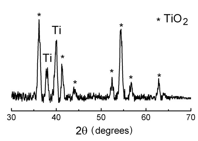
The structure of the films was determined by performing X-ray incident beam experiment with Cu tube (λ = 1.5406 Å). In Figure 1, there are presented XRD patterns of a PTL and a PML samples. The fact that the peak width is rather large shows that both the TiO2 and MoO3 layers were formed by nanocrystalline grains. Besides, the appearance of the intensive peaks of the titanium and molybdenum on the XRD patterns proves that X-ray went through the TiO2 and MoO3 layers and interacted
Table 1. The thickness of the layers for heterojunctions and devices.

 (a)
(a)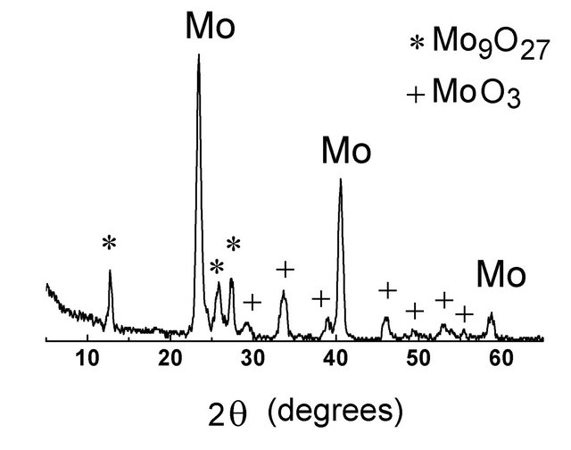 (b)
(b)
Figure 1. XRD patterns of a metallic Ti and Mo wafers annealed 1.5 h, at 700˚C and 500˚C, respectively, showing nanocrystalline TiO2 and MoO3 grown on Ti-wafer surface (a) and Mo-wafer surface (b).
with the titanium and molybdenum crystalline lattice. Although the metallic oxide layers are thin (~150 nm), in the XRD patterns all the key characteristic peaks of a rutile TiO2 crystal are revealed, those are peaks denoted by “star” symbols in Figure 1(a) (PDF card No. 00-021- 1276). In the XRD patterns of the annealed Mo-wafer (Figure 1(b)) there are seven diffraction peaks (denoted by “plus” symbols) corresponding MoO3 (PDF card No. 00-005-0508) and three other peaks (“star” symbol) characterize a crystalline structure of Mo9O27 (PDF card No. 00-012-0753) that was also formed upon annealing.
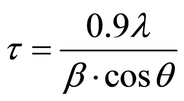
To determine the grain size (τ), we used Scherrer’s formula [14]:
 (1)
(1)
where λ is X-ray wavelength used, β is the full width at half maximum in radians, and θ is the Bragg angle of the considered diffraction peak. The average value of the particles calculated from XRD peaks was found to be of ca. 30 nm for the PTL and 40 nm for the PML sample.
The surface morphology of PML and PTL samples is revealed by FE-SEM micrographs (Figure 2). This figure shows the porous molybdenum and titanium surface layers, where Mo and Ti oxides were grown in form of nanorods. The images in Figure 2 reflect such a high resolution of the FE-SEM, that from them, one can determine approximately both the size on the surface and the length of TiO2 and MoO3 nanorods grown in the Moand Ti-wafers. The PTL sample is much more porous than the PML. By measuring the width and length of the rods from the FE-SEM micrographs for both samples, one can determine an average value for the rods. The results show that TiO2 rods in the PTL sample have a width of ~30 nm and a length of about 100 nm; the rods of MoO3 in the PML are 35 nm in width and 120 nm in length. This result is in a good agreement with the data obtained from XRD patterns for the average size of grains. In the PTL a large number of the rods have orientation close to the vertical direction (Figure 2(a)), whereas in the PML (Figure 2(b)) MoO3 rods were randomly orientated.
We also annealed Ti and Mo wafers at temperatures of 400˚C and 800˚C. Even with different annealing processes, the features of the nanorods on molybdenum and titanium substrates were similar to those for PML. This shows that for growing nanorod-like MoO3 and TiO2 on metallic molybdenum and titanium surfaces, the temperature can be maintained at 500˚C and 700˚C for 1.5 h, respectively. The PTL and PML layers further have been coated by NPB to get heterojunctions of NPB/nc-TiO2 and NPB/nc-MoO3. To characterize PL spectra of the NPB/nc-TiO2 and NPB/nc-MoO3 samples in comparison with the PL of the NPB/Ti and NPB/Mo ones, all the samples were put on the pathway of a He-Cd laser beam. The results of PL measurements of the samples excited at short wavelengths (namely 325 nm) are presented in Figure 3.
As seen in Figure 3, the PL intensity of the hybrid heterojunctions were increased in comparison with those of the polymer coated onto metallic wafes (NPB/Ti and NPB/Mo). This is similar to the reported results [15], when a nanorod-like composite of MEH-PPV + TiO2 was excited by photons of a large energy; its photoluminescence was enhanced in comparison with that of MEHPPV alone. Recently, we also observed the photoluminescent
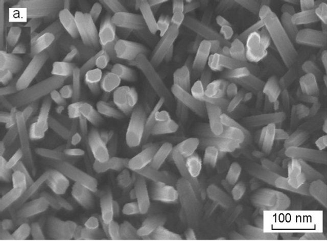
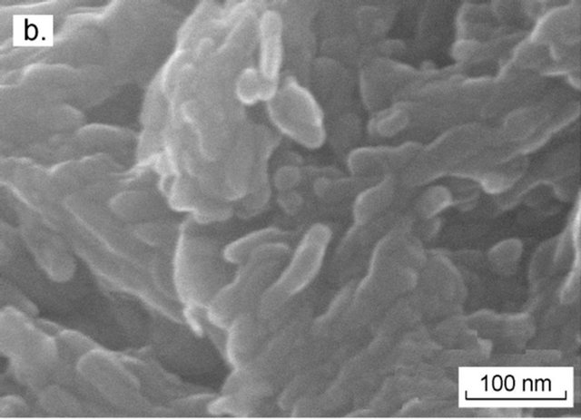
Figure 2. FE-SEM micrographs of Ti-wafer annealed at 700˚C for 1.5 h—PTL sample (a) and Mo-wafer annealed at 500˚C for 1.5 h—PML sample (b).

Figure 3. PL spectra of NPB/Mo (curve “1”), NPB/Ti (curve “2”), NPB/MoO3/Mo (curve “3”) and NPB/TiO2/Ti (curve “4”). Excitation wavelength λ = 325 nm.
enhancement of MEH-PPV/nc-TiO2 hybrid films [13]. From Figure 3, one can notice that all the samples have broad photoemission with a peak at 453 nm. A strongest PL enhancement occurred in NPB/nc-TiO2 film. In this hybrid film a small blue shift was observed, as it was obtained for MEH-PPV + nc-TiO2 [13] or for PPV + nc-SiO2 [16]. Although PL enhancement has been rarely mentioned, one can suggest that the increase PL intensity for such a PTL sample can be explained by the large absorption coefficient for TiO2 nanorods. This is similar to the effect observed for the MEH-PPV films, which is due to the non-radiative Förster resonant energy transfer [17] from TiO2 nanorods to polymer with excitation at a wavelength lesser than 350 nm. The obtained results on the photoluminescence for the hybrid samples indicate that the heterojunctions of NPB/nc-TiO2 and/or NPB/nc-MoO3 constituted a factor favouring electrons, which were generated in metallic oxide layers under the photon excitation, for faster transport in the polymeric layer. For measuring I-V and EL characteristics, the electrodes (anode and cathode) were connected to conducting wires by using a conductive silver paste. I-V characteristics of NPB/nc-TiO2/Ti and Al/Alq3/MADN/NPB/nc-MoO3/ Mo devices (abbreviated to TBD and MBD, respectively) showed that the turn-on voltage of the hybrid devices lowered from 5.4 V (standard device) to 4.8 V (TBD device) and 4.4 V (MBD device) (Figure 4).
The lowering of the turn-on voltage of hybrid deviecs may be explained due to following facts: 1) Ag/Mo and Ag/Ti contacts made from the silver paste are “metalto-metal”, consequently much better (more ohmic) than the Ag/ITO one (metal-to-oxide); 2) the work function of nc-MoO3 (6.80 eV [18]) is much larger than that of TiO2 (5.25 eV [19]) and ITO (4.50 eV [20]). This results in the decrease of the applied Dc bias, and also the increase of hole injection efficiency from the MoO3/Mo and TiO2/Ti electrodes to the hole transport layer (NPB).
The fact that the improvement in I-V of the TBD and MBD occurred due to replacing ITO by the thin MoO3 and TiO2 layers sandwiched between the polymer and metallic substrates proves that the nc-MoO3 and nc-TiO2
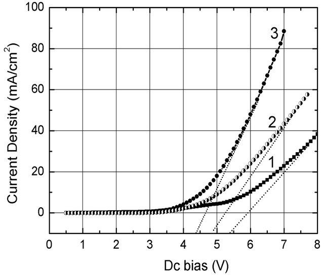
Figure 4. I-V characteristics of OLEDs made from different layers: (1) Al/Alq3/MADN/NPB/ITO (standard device); (2) Al/Alq3/MADN/NPB/nc-TiO2/Ti (TBD device); (3) Al/Alq3/ MADN/NPB/nc-MoO3/Mo (MBD device).
layers played the role of an anode for OLEDs. For such OLEDs, instead of the transparent anode like the ITO used, a semi-transparent or transparent Al-cathode was coated on the device top.
To compare luminous efficiency (ξ) of TBD and MBD devices with the Al/Alq3/MADN/NPB/ITO (standard device), all the Al-coatings were prepared with the same thickness, namely 45 nm; their transmittance in the wavelength region from 480 nm to 560 nm reached a value as large as 55%. The ξ-V curves are plotted in Figure 5. To compare ξ of the hybrid OLEDs with the one of the standard device, the ITO surface was absolutely dark-covered. The fact that the features of the I-V (Figure 4) and ξ-V curves (Figure 5) are quite similar proves that the efficient performance of an OLED can be preliminarily estimated from the I-V characteristics.
Indeed, the abrupt increase in luminous efficiency related to the most effective current corresponding to the turn-on voltage, where the current density raised with an abrupt value.
Comparing ξ-V curves of the devices, one can clearly see that ξ of heterojunction-based devices is much larger than the one of the standard device.
At a Dc bias of 6 V, the luminous efficiency of the TBD and MBD device reached a value as large as ~0.16 cd/A and ~0.73 cd/A, respectively. Whereas, for the standard device ξ » 0.23 cd/A in case the emission light is collected from the semitransparent cathode (Al-cathode).
The result of the ξ-V measurements on the standard device with the light collection from the ITO anode (Figure 6, curve “1b”) shows a ξ much larger, namely 1.50 cd/A (at 6 V)—more than 6 times larger than ξ obtained in the case of the semitransparent cathode (Figure 6, curve “1a”). This demonstrates that the Al-cathode reflected back a large part of the emission light. Thus, one can qualitatively estimate that for the heterojunctionbased OLEDs the luminous efficiency may attain a large value up to ~1.0 cd/A (with nc-TiO2/Ti based device) and ~4.3 cd/A—more than 15 times larger than ξ of the standard device (with nc-MoO3/Mo based device) in case the transparent cathode is successfully coated onto the ETL layer.
4. Conclusions
Nanostructured hybrid layers of NPB/TiO2 and NPB/ MoO3 were prepared by coating NPB onto nanorod-like TiO2 and MoO3 films thermally grown from titanium and molybdenum wafers. The nanocrystalline structure of the MoO3 and TiO2 films was revealed by XRD analysis; the size of the nanorods measured on FE-SEM was found to be of 30 nm in width and 100 nm in length for TiO2, and 35 nm in width and 120 nm in length for MoO3. In comparison with a pure NPB, under excitation of a largeenergy photon beam (λ = 325 nm), the intensity of the PL
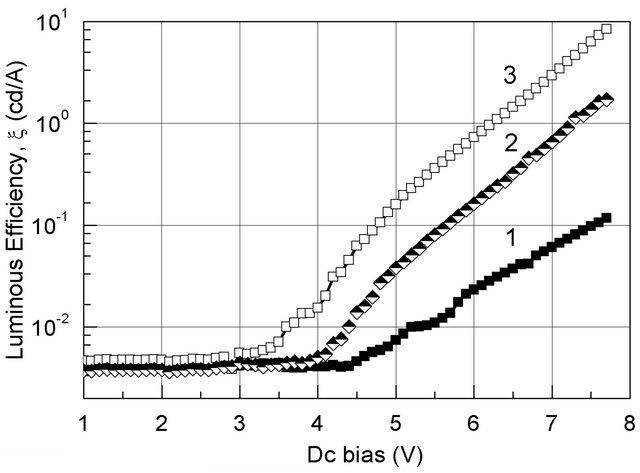
Figure 5. Luminous efficiency (x) vs. Dc bias of B-OLEDs for the standard (1), TBD (2) and MBD devices (3).
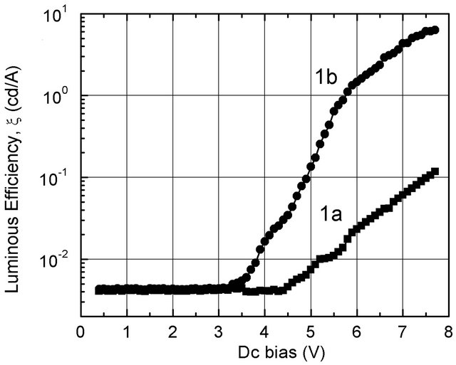
Figure 6. x-V plots of the standard device obtained from light emitting through Al-cathode (1a) and ITO anode (1b).
spectra of the hybrid layers considerably increased.
The turn-on voltage of the devices was found to be lowering from 5.4 V (for a standard B-OLED) to 4.8 V (for Al/Alq3/MADN/NPB/nc-TiO2/Ti) and 4.4 V (for Al/Alq3/MADN/NPB/nc-MoO3/Mo). The electroluminous efficiency of the hybrid devices was considerably enhanced in comparison with the standard device. This suggests a useful application for fabricating “reverse” OLEDs, where the emission light goes-out through the semitransparent cathode, instead of the ITO anode. Moreover, the ohmic contacts of conducting wires to metallic electrodes can be made much better than to the ITO anode.
To research technology for depositing an electrically conducting transparent cathode onto the electron transport layer is the aim of our further work.
5. Acknowledgements
Financial support by Vietnam Ministry of Science and Technology (1/2010/HD-DTNCCBUD) is gratefully acknowledged. We are grateful to Dr. Hung Manh Do, Institute of Materials Science, Vietnamese Academy of Science and Technology for measuring FE-SEM micrographs. All the experimental data left were measured on the equipments which were invested by Vietnamese Government through a VNU project on “Nanotechnology and Application” in the period of 2010-2013.
REFERENCES
- J. S. Salafsky, “Exciton Dissociation, Charge Transport, and Recombination in Ultrathin, Conjugated Polymer, TiO2 Nanocrystal Intermixed Composites,” Physical Review B, Vol. 59, No. 16, 1999, pp. 10885-10894. doi:10.1103/PhysRevB.59.10885
- W. U. Huynh, J. J. Dittmer and A. P. Alivisatos, “Hybrid Nanorod, Polymer Solar Cells,” Science, Vol. 295, No. 5564, 2002, pp. 2425-2427. doi:10.1126/science.1069156
- J. Dittmer, R. Lazzaroni, P. Leclere, P. Moretti, M. Granstrom, K. Petritsch, E. A. Marseglia, R. H. Friend, J. L. Bredas, H. Rost and A. B. Holmes, “Crystal Network Formation in Organic Solar Cells,” Solar Energy Materials and Solar Cells, Vol. 61, 2000, pp. 53-61. doi:10.1016/S0927-0248(99)00096-3
- V. M. Burlakov, K. Kawata, H. E. Assender, G. A. D. Briggs, A. Ruseckas and I. D. W. Samuel, “Discrete Hopping Model of Exciton Transport in Disordered Media,” Physical Review B, Vol. 72, No. 7, 2005, Article ID: 075206. doi:10.1103/PhysRevB.72.075206
- P. S. Thomas, J. Kuruvilla and T. Sabu, “Mechanical Properties of Titanium Dioxide-Filled Polystyrene Microcomposites,” Materials Letters, Vol. 58, No. 3-4, 2004, pp. 281-289. doi:10.1016/S0167-577X(03)00470-1
- S. A. Choulis, M. K. Mathai and V.-E. Choong, “Influence of Metallic Nanoparticles on the Performance of Organic Electrophosphorescence Devices,” Applied Physics Letters, Vol. 88, No. 21, 2006, Article ID: 213503. doi:10.1063/1.2200285
- S. A. Carter, J. C. Scott and J. Brock, “Enhanced Luminance in Polymer Composite Light Emitting Diodes,” Applied Physics Letters, Vol. 71, No. 9, 1997, pp. 1145-1147. doi:10.1063/1.119848
- A. Petrella, M. Tamborra, P. D. Cozzoli, M. L. Curri, M. Striccoli, P. Cosma, G. M. Farinola, F. Babudri, F. Naso and A. Agostiano, “TiO2 Nanocrystals—MEH-PPV Composite Thin Films as Photoactive Material,” Thin Solid Films, Vol. 451-452, 2004, pp. 64-68. doi:10.1016/j.tsf.2003.10.106
- A. A. Madhavan, G. G. Kumar, S. Kalluri, J. Joseph, S. Nagarajan, S. Nair, K. R. V. Subramanian and A. Balakrishnan, “Effect of Embedded Plasmonic Au Nanoparticles on Photocatalysis of Electrospun TiO2 Nanofibers,” Journal of Nanoscience and Nanotechnology, Vol. 12, No. 10, 2012, pp. 7963-7967. doi:10.1166/jnn.2012.6492
- K. J. Klabunde, “Nanoscale Materials in Chemistry,” John Wiley & Sons, Hoboken, 2001. doi:10.1002/0471220620
- R. Nirmala, J. W. Jeong, R. Navamathavan and H. Y. Kim, “Synthesis and Electrical Properties of TiO2 Nanoparticles Embedded in Polyamide-6 Nanofibers via Electrospinning,” Nano-Micro Letters, Vol. 3, No. 1, 2011, pp. 56-61.
- N. N. Dinh, L. H. Chi, T. T. Chung-Thuy, T. Q. Trung and Vo-Van Truong, “Enhancement of Current-Voltage Characteristics of Multilayer Organic Light Emitting Diods by Using Nanostructured Composite Films,” Journal of Applied Physics, Vol. 105, 2009, pp. 093518-1- 093518-5.
- T. T. Chung-Thuy, L. H. Chi and N. N. Dinh, “Study of Photoluminescent and Electrical Properties of Nanostructured MEH-PPV/TiO2 Hybrid Films,” JKPS, Vol. 54, 2009, pp. 291-295. doi:10.3938/jkps.54.291
- B. D. Cullity, “Elements of X-Ray Diffraction,” 2nd Edition, Addison-Wesley Publishing Company, Boston, 1978,
- Y. T. Lin, T. W Zeng, W. Z. Lai, C. W. Chen, Y. Y. Lin, Y. S. Chang and W. F. Su, “Efficient Photoinduced Charge Transfer in TiO2 Nano-Rod/Conjugated Polymer Hybrid Materials,” Nanotechnology, Vol. 17, No. 23, 2006, pp. 5781-5785. doi:10.1088/0957-4484/17/23/012
- S. H. Yang, T. P. Nguyen, P. Le Rendu and C. S. Hsu, “Optical and Electrical Properties of PPV/SiO2 and PPV/ TiO2 Composite Materials,” Composites Part A: Applied Science and Manufacturing, Vol. 36, No. 4, 2005, pp. 509-513. doi:10.1016/j.compositesa.2004.10.008
- G. Heliotis, G. Itskos, R. Murray, M. D. Daw-Son, I. M. Watson and D. D. C. Bradley, “Hybrid Inorganic/Organic Semiconductor Heterostructures with Efficient Non-Radiative Energy Transfer,” Advanced Materials, Vol. 18, No. 3, 2006, pp. 334-338. doi:10.1002/adma.200501949
- Z. Chen, I. Santoso, R. Wang, L. F. Xie, H. Y. Mao, H. Huang, Y. Z. Wang, X. Y. Gao, Z. K. Chen, D. Ma, A. T. S. Wee and W. Chen, “Surface Transfer Hole Doping of Epitaxial Graphene Using MoO3 Thin Film,” Applied Physics Letters, Vol. 96, No. 21, 2010, pp. 213104- 213107. doi:10.1063/1.3441263
- S. Gutmann, M. A. Wolak, M. Conrad, M. M. Beerbom and R. Schlaf, “Effect of Ultraviolet and X-Ray Radiation on the Work Function of TiO2 surfaces,” Journal of Applied Physics, Vol. 107, No. 10, 2010, pp. 103705-103708. doi:10.1063/1.3410677
- R. Schlaf, H. Murata and Z. H. Kafafi, “Work Function Measurements on Indium Tin Oxide Films,” Journal of Electron Spectroscopy and Related Phenomena, Vol. 120, No. 1-3, 2001, pp. 149-154. doi:10.1016/S0368-2048(01)00310-3

