Materials Sciences and Applications
Vol. 3 No. 11 (2012) , Article ID: 24939 , 8 pages DOI:10.4236/msa.2012.311117
Future Semiconductor Devices for Multi-Valued Logic Circuit Design
![]()
1Intel Corporation, Hillsboro, USA; 2Department of Electrical & Computer Engineering, University of Connecticut, Storrs, USA.
Email: *mr.karmakar@yahoo.com
Received August 6th, 2012; revised September 7th, 2012; accepted October 5th, 2012
Keywords: MVL; Quantum Dots; FET; QDCFET; QDGFET; SWSFET
ABSTRACT
This paper introduces future devices for multi-valued logic implementation. Quantum dot gate field effect transistor (QDGFET) works based on the change in threshold voltage due to stored charge in the quantum dots in the gate region. Quantum dot channel field effect transistor (QDCFET) produces more number of states in their transfer characteristics because of charge flow through the mini-band structure formed by the overlapping energy bands of the neighboring quantum dots in the channel region of the FET. On the other hand spatial wave-function switched field effect transistor (SWSFET) produces more number of states in its transfer characteristic based on the switching of charge carriers from one channel to other channel of the device. In this paper we discuss QDGFET, QDCFET and SWSFET in detail to explore their application in future multi-valued logic circuits.
1. Introduction
The basic building block to implement binary logic is the metal-oxide-semiconductor field-effect transistor (MOSFET). The trend predicted by Moore’s Law has called for these MOS devices to shrink in half every 18 - 24 months [1,2]. As feature sizes have started to approach sub-22 nm regime, several issues have begun to make further miniaturization difficult [3-5]. As transistors have decreased in size, the thickness of the gate dielectric needs to be decreased to increase the gate capacitance, and thereby the drive current and device performance [6-9]. As the gate dielectric thickness is scaled down below 2 nm, leakage currents due to the tunneling of charge carriers increase drastically, which increases the unwieldy power consumption of the device and reduces device reliability [10-12]. Another approach to increase integration is to increase the bit handling capacity of a fabricated device. Traditional MOSFETs can only process one bit at a time.
Higher level of bit density can be achieved using multi-valued logic (MVL) [13]. Multi-value logic is defined as a non-binary logic and involves the switching between more than 2 states.
Research is ongoing towards the development of devices that are suitable for multi-valued operation. Resonant tunneling transistors (RTTs) [14-16] and resonant tunneling diodes (RTDs) [17,18] are the major promising semiconductor devices for MVL applications. All these devices produce negative differential resistance (NDR) in the specific voltage range of operations.
All the devices that have been proposed so far however, until now are not matured yet for MVL circuit implementation. These devices have more serious problems than complementary metal-oxide-semiconductor (CMOS) devices, such as excess leakage current, being unable to operate at room temperature, or requiring complex fabrication processes. Research is ongoing to find a better combination of stack materials for resonant tunneling devices. A common problem in the NDR devices is to reduce the valley current, which is due to the unintentional excess leakage current. In this paper we propose some new devices which can be promising circuit element in future to implement multi-valued logic with better performance. Before discussing new devices, we will highlight other two existing devices like resonant tunneling diode (RTD) and resonant tunneling transistor (RTT) in Sections 2 and 3. Three new devices, quantum dot gate field effect transistor (QDGFET), quantum dot channel field effect transistor (QDCFET) and spatial wave-function switched field effect transistor (SWSFET) are discussed in Section 4 which is followed by conclusions in Section 5.
2. Resonant Tunneling Diode (RTD)
A resonant tunneling device is similar in construction to a p-n junction diode with two terminals [19]. The device has a quantum well layer separated from two conducting regions by quantum barriers (on the order of 50 Å to 100 Å thick). The barriers can be higher bandgap AlGaAs, for example, while the well and conduction regions can be lower bandgap GaAs.
Electrons tunnel through two barriers separated by a well when flowing from source to drain in a resonant tunneling diode, which is also known as quantum mechanical tunneling [20]. The flow of electrons is controlled by diode bias. This matches the energy levels of the electrons in the source to the quantized level in the well so that electrons can tunnel through the barriers. The energy level in the well is quantized because the well is small. When the energy levels are equal, a resonance occurs, which allows electron flow through the barriers as shown in Figure 1(b). No bias or too much bias, in Figures 1(a) and (c) respectively, yields an energy mismatch between the source and the well, and electrons can not conduct.
When the bias is increased from zero across the RTD, the current increases, then decreases, correspond to off, on and off states. Figure 2 shows the I-V characteristic of a resonant tunneling diode. This makes simplification of conventional transistor circuits possible by substituteing a pair of RTD for two transistors. The potential application of RTD is to reduce the component count, area, and power dissipation of conventional transistor circuits by replacing some, though not all, transistors.
RTDs have allowed us to realize certain applications that will be beyond the capability of CMOS technology [21,22]. These low-power, high speed, and small devices are especially important as we continue to scale down to the size of atoms, where heat and parasitic effects are a major problem. However, in order for RTD to reach its full potential, more mature fabrication techniques are necessary. Precise barrier thickness control is required to ensure uniformity across the whole wafer. Also, the output power of RTDs is limited. More research is required to realize RTD circuits without an amplifier or other drivers. This will minimize the power and area of the integrated circuit (IC).
3. Resonant Tunneling Transistor (RTT)
A Resonant Tunneling Transistor [23] is similar to the resonant tunneling device which has source, drain and a gate electrode attached to its well region [24]. Electrons are injected into the device through the source electrode. An applied gate voltage adjusts the energy of the well levels with respect to the energy range of the occupied conduction states in the source region. Carriers tunnel through the barrier into the well from the source region when the energy of a well state falls within the energy
 (a)
(a)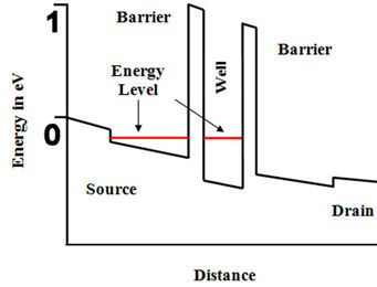 (b)
(b) (c)
(c)
Figure 1. Resonant tunneling diode (RTD): (a) No bias, source and well energy levels not matched, no conduction. (b) Small bias causes matched energy levels (resonance); conduction results. (c) Further bias mismatches energy levels, decreasing conduction.
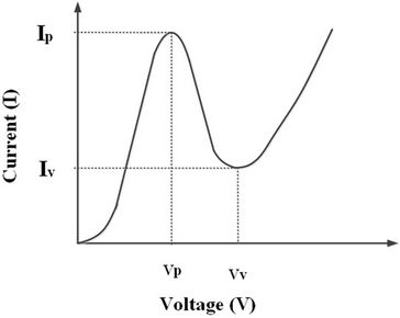
Figure 2. RTD I-V characteristic.
range of the occupied conduction states in the source [25, 26]. With a voltage applied from the source region to drain region, the charge then flows into the drain region.
4. New Proposed Devices
4.1. Quantum Dot Gate Field Effect Transistor (QDGFET)
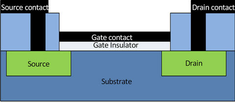
The device structure of a quantum dot gate field effect transistor (QDGFET) is shown in Figure 3(b). Unlike conventional FET (Figure 3(a)), a quantum dot layer is deposited on top of the gate insulator in QDGFET.
FEI Strata 400S Dual-Beam FIB instrument was used to prepare the sample for cross-sectional TEM imaging. A 1 µm thick membrane having dimension of 10 µm across and 5 µm in height was cut through the sample using Ga+ ion beam. Platinum layer was deposited onto the surface of the FET to minimize the ion beam damage to the device during FIB machining.
A JEOL 2010 FasTEM was used to examine the TEM specimens. This instrument is equipped with a high-resolution objective lens pole-piece and operate at 200 kV and produce a point-to-point resolution of <0.19 nm in phase contrast images. Chemical microanalysis was also performed in situ using an EDAX Phoenix atmospheric thin window EDXS. TEM image (Figure 4) obtained from the experiment shows the deposition of two layers of SiOx cladded-Si quantum dots in the gate region of the QDGFET.
QDGFETs exhibit an intermediate state between “ON” and “OFF” states in their transfer characteristic because of stored charge in the quantum dots in the gate region.
 (a)
(a)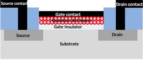 (b)
(b)
Figure 3. Cross-sectional schematic of (a) conventional FET, (b) quantum dot gate FET (QDGFET).
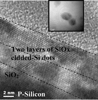
Figure 4. HRTEM picture of fabricated QDGFET, (inset) TEM image of fabricated SiOx-Si quantum dots.
In the intermediate state the drain current (ID) is independent over a range of gate voltages, which is determined by the thicknesses of tunnel gate insulator, quantum dot cladding as well as their core diameter [27-29].
This novel three-state characteristic of QDGFET provides new versatility in designing MVL implementation with significantly reduced FET counts. In previous work, we have shown the usage of these novel transistors in the construction of three state complement functions and memory cells [30]. Different ternary logics can be implemented using this three state property of the QDGEFT.
Theory of Operation
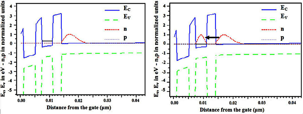
Figures 5(a)-(d) show the energy band diagrams and the carrier concentration plots in the quantum well channel and two quantum dot gate layers at various gate voltages. Figure 5(a) shows the state of the device at a gate voltage before the dots are charged. In Figure 5(b), the first layer of dots closest to the channel is charged via tunneling of charge carriers from inversion channel. The buildup of the charge in the first quantum dot layer as the energy levels in the second quantum dot layer are not lined up is shown in Figure 5(c). In Figure 5(d), the resonant tunneling occurs to the second quantum dot layer due to alignment of the bound states in the first quantum dot layer and the second quantum dot layer. Table 1 shows different simulation parameters for device simulation.
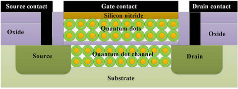
4.2. Quantum Dot Channel Field Effect Transistor (QDCFET)
Quantum dot channel FET (QDCFET) is another promising circuit element to implement MVL. Jain et al. [31, 32] already discussed the fabrication and theory of operation of QDCFET. The structural difference between a QDCFET and a conventional FET is the presence of
 (a)
(a)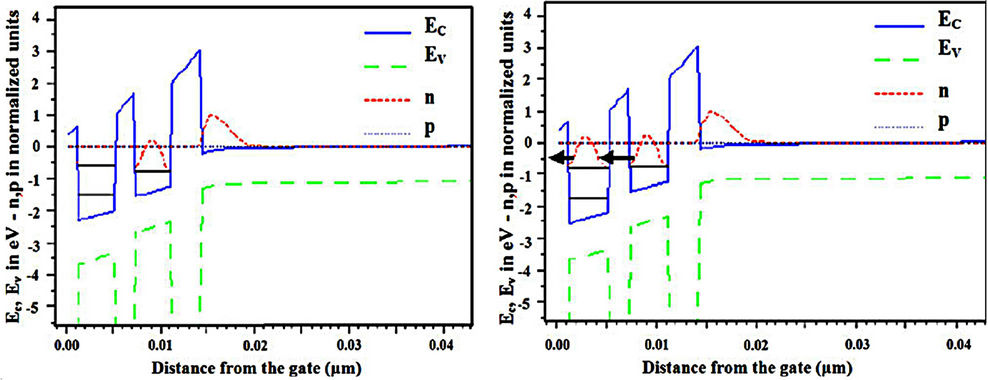 (b)
(b)
Figure 5. Device simulation shows the tunneling of electron wave function from inversion channel to different quantum dot layers when gate voltage increases from (a) to (d) gradually [30].
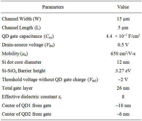
Table 1. QDGFET parameters for charge control simulation.
quantum dot layers between the source and drain region in the QDCFET. The presence of quantum dots in the channel region produces four states in the transfer characteristic of the QDCFET which can be used to implement four state inverter and MVL.
The device structure of a QDCFET is shown in Figure 6(a). The presence of quantum dots in the channel region is shown in Figure 6(b).
The current transport in a QDCFET depends on the carrier concentration in the inversion layer and their transport in the quantum dot channel as a function of the gate voltage [32]. Quantum dots inside the channel formed like a super lattice. The transfer of the charge carriers from the source to the drain region of QDCFET depends on the mini band structure formed by overlapping of energy bands of different quantum dots in the channel region. These mini-bands are occupied by charge carriers based on the drain-to-source voltage (VDS). As
 (a)
(a)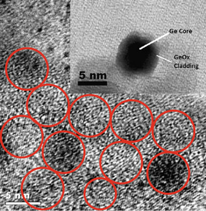 (b)
(b)
Figure 6. (a) The device structure of a QDCFFET, (b) HRTEM image of quantum dots in the channel region of QDCFET, (Inset) TEM image of GeOx cladded-Ge quantum dots.
VDS is increased, the next level of mini-band is filled and charge flows through both mini-bands. The quantum dots in the gate region change the threshold voltage of the device because of tunneling of the charge carriers from the quantum dot channel to the quantum dot layer in the gate region. The generation of the steps in the transfer characteristic of QDCFET is the cumulative effects of the quantum dots in the channel region as well as in the gate region of the device. Figure 7 shows the transfer characteristic of a fabricated QDCFET having four states in its transfer characteristic. The two intermediates states are at around 1.6 V and 2.15 V of gate voltage which is shown in Figure 7.
The generation of four states in the transfer characteristic of a QDCFET can be used to implement quaternary logic in future. More research is necessary to explore this device as a circuit element to implement multi-valued logic in future.
4.3. Spatial Wave-Function Switched FET (SWSFET)
Spatial wave-function switched (SWS) FET is a promis-
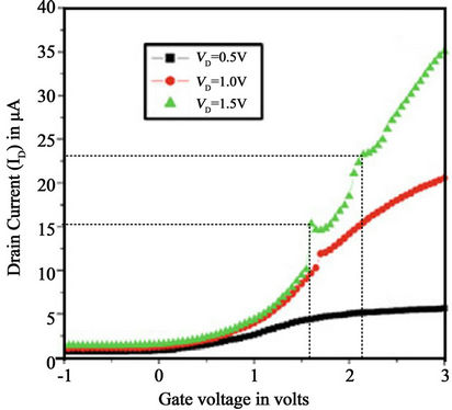
Figure 7. ID vs. VGS characteristic of a fabricated QDCFET.
ing circuit element for digital integrated circuits. Based on the applied gate voltage, the charge flows through different channels in a SWSFET. When the gate voltage is low but above the threshold voltage (Vth1) of the device, charge carriers are confined in the lower quantum well channel and flows from source to drain region. As the gate voltage is increased (Vth2), charge carriers transfer from the lower channel to the upper quantum well channel and current flows through the upper channel of the device. The device structure of a SWSFET is shown in Figure 8. Based on the applied gate voltage, the electron concentration as well as the electron wave function switches from one channel to the other channel and current flows through different drain terminals.
The energy band-diagram of the SWSFET is schematically shown in Figure 9 [33]. Figure 10 shows the capacitance-voltage (C-V) characteristics of a fabricated two quantum well channel InGaAs-AlInAs SWSFET [33]. The C-V curves show distinct peak before the accumulation regime (gate voltage less than –2V) where the capacitance becomes constant. The capacitance of the SWS device reaches to first maximum value at a gate voltage ~–0.1 V. This occurs when the holes are in the lower quantum well channel #1. When the gate voltage is reduced further, holes are transferred from the first quantum well layer (channel #1) to the second quantum well layer (channel #2). The capacitance increases as the carriers are in the proximity of gate until total accumulation is reached. The detailed device operation is already published elsewhere [33].
The circuit model of a SWSFET is developed in Berkeley short channel IGFET model (BSIM 3). In the circuit model, SWSFET effect is introduced by modifying the threshold voltage of conventional FET model in BSIM. The simulated transient characteristic of the SWSFET model is shown in Figure 11 [34,35]. Because of two drain terminals, a two-channel SWSFET is also

Figure 8. Device structure of SWSFET.
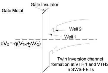
Figure 9. Energy band diagram of a SWSFET [33].
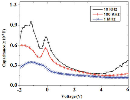
Figure 10. C-V characteristics of SWSFET [35].

Figure 11. Transfer characteristic of the SWSFET model [34,35].
known as a twin-drain SWSFET. In this simulation we connect two drains of the twin SWSFET and simulate the transfer characteristic (ID vs. VGS) of the device. The simulation result shows that the drain current initially flows through the lower channel which is farther from the gate terminal. When the gate voltage increases further, charge carriers transfer from the lower channel to the upper channel (closer to the gate terminal) and current flows decreases in the lower channel and increases in the upper channel and ultimately all current flows through the upper channel.
5. Conclusion
In this paper, we introduce three new devices to implement multi-valued logic in future. These devices produce more stable output because of the cladded quantum dots in their structure. All these devices work based on different mechanism of charge storage in their device structure. In QDGFET, three states generate because of stored charge in the quantum dots in the gate region. Whereas in QDCFET, the multi-states generate because of formation of mini band structure in the channel region and the stored charge in the gate region. In the SWSFET, the multi valued logic can be implemented base on the charge in different quantum well channel in their device structure. The improved noise margin and the existing CMOS fabrication mechanism can make these quantum dot based devices as promising circuit element for multi valued logic implementation in future.
REFERENCES
- G. E. Moore, “Cramming More Components onto Integrated Circuits,” Electronics, Vol. 38, No. 8, 1965, pp. 114-117.
- G. E. Moore, “No Exponential Is Forever: But ‘Forever’ Can Be Delayed!” Solid-State Circuits Conference, IEEE International Digest of Technical Papers, Vol. 1, 2003, pp. 20-23. doi:10.1109/ISSCC.2003.1234194
- E. J. Nowak, “Maintaining the Benefits of CMOS Scaling When Scaling Bogs Down,” Journal of Research and Development, Vol. 46, No. 2-3, 2002, pp. 169-180.
- T. N. Theis, “Beyond the Silicon Transistor: Personal Observations,” Computing in Science & Engineering, Vol. 5, No. 1, 2003, pp. 25-29.
- S. Borkar, “Design Perspectives on 22 nm CMOS and beyond,” Design Automation Conference, San Francisco, 26-31 July 2009, pp. 93-94.
- M. Goto, S. Kawanaka, S. Inumiya, N. Kusunoki, M. Saitoh, K. Tatsumura, A. Kinoshita, S. Inaba and Y. Toyoshima, “The Study of Mobility-Tin, Trade-Off in Deeply Scaled High-k/Metal Gate Devices and Scaling Design Guideline for 22 nm-Node Generation,” 2009 Symposium on VLSI Technology, Kyoto, 16-18 June 2009, pp. 214-215.
- R. Huang, H. M. Wu, J. F. Kang, D. Y. Xiao, X. L. Shi, X. An, Y. Tian, R. S. Wang, L. L. Zhang, X. Zhang, et al., “Challenges of 22 nm and beyond CMOS Technology,” Science in China Series F: Information Sciences, Vol. 52, No. 9, 2009, pp. 1491-1533.
- S. Thompson, et al., “A 90 nm Logic Technology Featuring 50 nm Strained Silicon Channel Transistors, 7 Layers of Cu Interconnects, Low k ILD, and 1 μm2 SRAM Cell,” International Electron Devices Meeting Technical Digest, Vol. 6, 2002, pp. 61-64.
- K. Mistry, et al., “A 45 nm Logic Technology with High-k + Metal Gate Transistors, Strained Silicon, 9 Cu Interconnect Layers, 193 nm Dry Patterning, and 100% Pb-Free Packaging,” International Electron Devices Meeting Technical Digest, Washington DC, 10-12 December 2007, pp. 247-250.
- P. Bai, et al., “A 65 nm Logic Technology Featuring 35 nm Gate Lengths, Enhanced Channel Strain, 8 Cu Interconnect Layers, Low-k ILD and 0.57 μm2 SRAM Cell,” International Electron Devices Meeting Technical Digest, San Francisco, 13-15 December 2004, pp. 657-660.
- H. K. Lim and J. G. Fossum, “Threshold Voltage of ThinFilm Silicon-on-Insulator (SOI) Mosfet’s,” IEEE Transactions on Electron Devices, Vol. 30, No. 10, 1983, pp. 1244-1251. doi:10.1109/T-ED.1983.21282
- J. P. Colinge, “Transconductance of Silicon-on-Insulator Mosfets,” IEEE Electron Device Letters, Vol. EDL-6, 1985, pp. 573-574. doi:10.1109/EDL.1985.26234
- L. J. Micheel, A. H. Taddiken and A. C. Seabaugh, “Multiple-Valued Logic Computation Circuits Using Microand Nanoelectronics Devices,” Proceedings of 23rd IEEE International Symposium on Multiple-Valued Logic, Sacramento, 24-27 May 1993, pp. 164-169.
- A. C. Seabaugh, W. R. Frensley, J. N. Randall, M. A. Reed, D. L. Farrington and R. J. Matyi, “Pseudomorphic Bipolar Quantum Resonant-Tunneling Transistor,” IEEE Transaction on Electron Devices, Vol. 36, No. 10, 1989, pp. 2228-2234.
- J. Stock, J. Malindretos, K. M. Indlekofer, M. Pottgens, A. Forster and H. Luth, “A Vertical Resonant Tunneling Transistor for Application in Digital Logic Circuits,” IEEE Transaction on Electron Devices, Vol. 48, No. 6, 2001, pp. 1028-1032.
- F. Capasso and R. A. Kiehl, “Resonant Tunneling Transistor with Quantum Well Base and High-Energy Injection: A New Negative Differential Resistance Device”, Journal of Applied Physics, Vol. 58, No. 3, 1985, pp. 1366-1368.
- H. C. Lin, “Resonant Tunneling Diodes for Multi-Valued Digital Applications,” Proceedings of 24th IEEE International Symposium on Multiple-Valued Logic, Boston, 25- 27 May 1994, pp. 188-195.
- A. Forster, “Resonant Tunneling Diodes: The Effect of Structural Properties on Their Performance,” Advances in Solid State Physics, Vol. 33, 1993, pp. 37-62.
- T. Waho, K. J. Chen and M. Yamamoto, “ResonantTunneling Diode and HEMT Logic Circuits with Multiple Thresholds and Multi-Level Output,” IEEE Journal of Solid-State Circuits, Vol. 33, No. 2, 1998, pp. 268-274.
- H. C. Lin, “Resonant Tunneling Diodes for Multi-Valued Digital Applications,” Proceedings of 24th IEEE International Symposium on Multiple-Valued Logic, Boston, 25- 27 May 1994, pp. 188-195.
- P. Mazumder, S. Kulkarni, M. Bhattacharya, J. P. Sun and G. I. Haddad, “Digital Circuit Applications of Resonant Tunneling Diodes,” Proceedings of IEEE, Vol. 86, No. 4, 1998, pp. 664-686. doi:10.1109/5.663544
- J. P. A. van der Wagt, H. Tang, T. P. E. Broekaert, A. C. Seabaugh and Y.-C. Kao, “Multibit Resonant Tunneling Diode SRAM Cell Based on Slew-Rate Addressing,” IEEE Transactions on Electron Devices, Vol. 46, No. 1, 1999, p. 5562. doi:10.1109/16.737441
- T. Waho, “Resonant Tunneling Transistor and Its Application to Multiple-Valued Logic Circuits,” Proceedings of 25th IEEE International Symposium on Multiple-Valued Logic, 1995, pp. 130-138.
- W. L. Chen, G. O. Mums, L. Davis, P. K. Bhattacharya and G. I. Haddad, “The Growth of Resonant Tunneling Hot Electron Transistors Using Chemical Beam Epitaxy,” The 4th International Conference in Chemical Beam Epitaxy, Section S-7, Nara, 21-23 July 1993.
- T. Futatsugi, Y. Yamaguchi, K. Ishii, K. Imamura, S. Muto, N. Yokoyama and A. Shibatomi, “A Resonant Tunneling Bipolar Transistor (RBT): A Proposal and Demonstration for New Functional Device with High Current Gains,” International Electron Devices Meeting Technical Digest, Washington DC, 7-10 December 1986, p. 286.
- A. C. Seabaugh, W. R. Frensley, Y. C. Kao, J. N. Randall and M. A. Reed, “Quantum-Well Resonant Tunneling Transistors,” The Proceedings of the 1989 IEEE Conference, Ithaca, 1989, p. 255.
- S. Karmakar, M. Gogna, E. Suarez, F. Alamoody, E. Heller, J. chandy and F. Jain, “3-State Behavior of Quantum Dot Gate FETs with Lattice Matched Insulator,” Proceedings of 2009 Nanoelectronic Devices for Defense and Security, Fort Lauderdale, 28 September-2 October 2009.
- S. Karmakar, J. A. Chandy and F. C. Jain, “Application of 25 nm Quantum Dot Gate FETs to the Design of ADC and DAC Circuits,” International Journal of High Speed Electronics and Systems, Vol. 20, No. 3, 2011, p. 653.
- S. Karmakar, A. P. Suresh, J. A. Chandy and F. C. Jain, “Design of ADCs and DACs Using 3-State Quantum DOT Gate FETs,” Proceedings of International Semiconductor Device Research Symposium, College Park, 9-11 December 2009.
- S. Karmakar, E. Suarez and F. Jain, “Quantum Dot Gate Three State FETs Using ZnS-ZnMgS Lattice-Matched Gate Insulator on Silicon,” Journal of Electronic Materials, Vol. 40, No. 8, 2011, pp. 1749-1756.
- F. Jain, S. Karmakar, R. A. Croce Jr., M. Gogna, E. Suarez, J. Chandy and E. Heller, “Multi-State Quantum Dot Channel (QDC) Field-Effect Transistors (FETs): A New Paradigm in Circuit Design,” 2011 Nanoelectronic Devices for Security Conference, Brooklyn, 29 August-1 September 2011.
- F. Jain, S. Karmakar, P.-Y. Chan, E. Suarez, M. Gogna, J. Chandy and E. Heller, “Quantum Dot Channel (QDC) Field-Effect Transistors (FETs) Using II-VI Barrier Layers,” Journal of Electronic Materials, Vol. 41, No. 10, 2012, pp. 2775-2784. doi:10.1007/s11664-012-2161-z
- F. C. Jain, B. Miller, E. Suarez, P.-Y. Chan, S. Karmakar, F. Al-Amoody, J. Chandy and E. Heller, “Spatial Wavefunction Switched (SWS) InGaAs FETs with II-VI Gate Insulators,” Journal of Electronic Materials, Vol. 40, No. 8, 2011, pp. 1717-1726. doi:10.1007/s11664-011-1667-0
- S. Karmakar, F. C. Jain, J. A. Chandy and E. Heller, “Circuit Model of SWSFET to Implement Multi-Valued Logic,” 21st CMOC Symposium, University of Connecticut, Storrs, 9 April 2012.
- S. Karmakar, J. A. Chandy and F. C. Jain, “Implementation of Unipolar Inverter Based on Spatial Wave-Function Switched (SWS) FET,” IEEE Lester Eastman Conference on High Performance Devices, Brown University, Providence, 7-9 August 2012.
NOTES
*Corresponding author.