Materials Sciences and Applications
Vol.3 No.8(2012), Article ID:21801,5 pages DOI:10.4236/msa.2012.38079
Microstructures and Photovoltaic Properties of Polysilane/C60-Based Solar Cells
![]()
Department of Materials Science, The University of Shiga Prefecture, Hikone, Japan.
Email: *oku@mat.usp.ac.jp
Received May 10th, 2012; revised June 12th, 2012; accepted July 9th, 2012
Keywords: Bulk heterojunction; Polysilane; Fullerene; Microstructure
ABSTRACT
Polysilane/C60-based solar cells were fabricated and investigated. Two-types of devices with bulk heterojunction and heterojunction structures were examined and characterized. Addition of silicon-based polymer to the organic solar cells improved the conversion efficiency by wide optical absorption and high carrier mobility. Microstructures of the solar cells were investigated by using X-ray diffraction and transmission electron microscopy. Energy levels in the present solar cells were discussed.
1. Introduction
Solar cells are one of the important candidates for renewable energy sources. Silicon (Si) solar cells which are the mainstream of renewable energy sources have highconversion efficiency with long lifetime. However, production processes are complicated, and the cost is high. Although organic thin film solar cells which are expected as an alternative to the Si-based solar cells have been investigated, the efficiencies have not been high enough for commercial application [1].
Recently, C60-based solar cells have been investigated and reported [2,3]. These organic solar cells have a potential for use in lightweight, flexible, inexpensive and large-scale solar cells [4-6]. By combining pand n-type organic semiconductors, the organic solar cells show wide wavelength absorption. However, significant improvements of photovoltaic efficiencies are mandatory for use in the future solar power plants. One of the improvements is to increase p-n heterojunction interface of the photoelectric conversion region in the devices by using blends of donor-like and acceptor-like molecules or polymers, which are called bulk heterojunction solar cells [7-9].
The bulk heterojunction solar cells based on copper tetrakis (4-cumylphenoxy) phthalocyanine (CuPc) with C60 have been studied in the previous work [10]. CuPc showed a wild optical absorption around 700 nm, which would suggest higher potential for photon harvesting. C60 has a property to attract an electron, which is suitable for solar cells. However, its conversion efficiency was not enough for commercial use, and it is necessary to improve the efficiencies of the solar cells further.
The purpose of the present work is to fabricate and characterize the CuPc/C60 solar cells with the Si-based polymers. The present work aimed at efficiency improvement for expansion of the absorption wavelength by silicon addition to CuPc/C60 solar cells. Two types of the Si-based polymers of poly [dimethylsiloxane-co-methyl (stearoyloxyalkyl) siloxane] (PDSi) and dimethylpolysilane (DMPS) were used. PDSi has been used as a nontoxicity and high resolvability. Polysilanes are σ-conjugated polymers exhibiting attractive characteristics such as photoconductivity, high hole mobility and effective light emission [11,12]. By blending C60 to polysilanes, it would suppress the recombination of photo-separated charge carriers by assisting the electron transfer from polysilanes [13]. The bulk heterojunction solar cells based on C60 with polysilane derivatives have also been studied [14]. To examine the additive effect of polysilane, DMPS/C60 solar cells were also produced. Device structures were produced, and the efficiencies, optical absorption and microstructure were investigated to improve efficiency of the organic solar cells with the polysilane.
2. Experimental Procedures
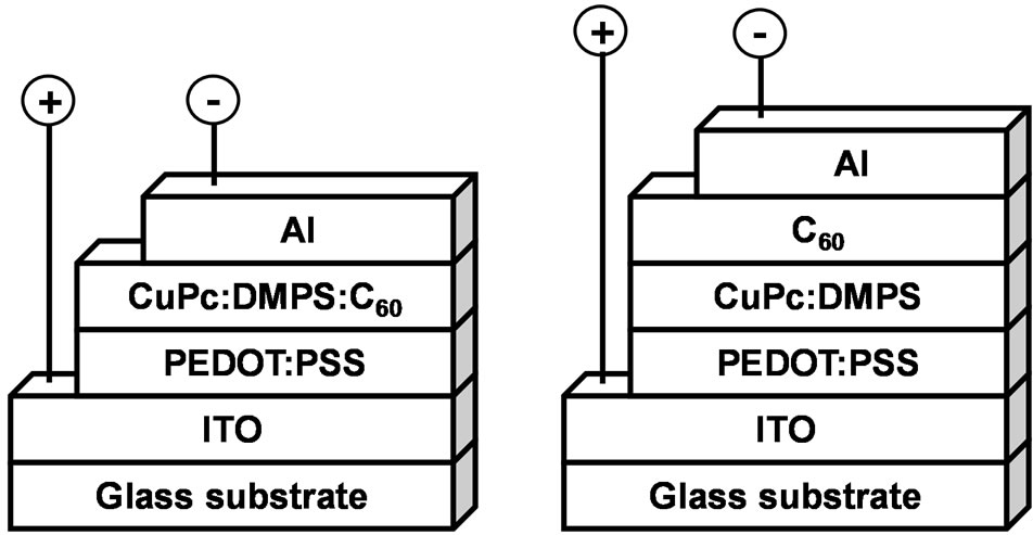
A thin layer of poly3,4-ethylenedioxythiophene doped with poly(-styrenesulfonate (PEDOT:PSS) (Sigma Aldrich) was spin-coated on pre-cleaned indium tin oxide (ITO) glass plates (Geomatec Co., Ltd., ~10 Ω/□). Then, semiconductor layers were prepared on a PEDOT:PSS layer by spin coating using a mixed solution of CuPc (Sigma Aldrich, 97%), C60 (Material Technologies Research, 99.98%) and PDSi (Sigma Aldrich) or DMPS (Strem Chemicals) in 1 ml o-dichlorobenzene. Weight ratios of CuPc:C60 were 1:8 (2 mg:16 mg), and PDSi (1 mg) or DMPS (3 mg) was added into the o-dichlorobenzene solution. The thickness of the blended device was approximately 150 nm. A schematic diagram of the bulk heterojunction solar cells of CuPc:(PDSi or DMPS): C60 is shown in Figure 1(a). Heterojunction solar cells were also fabricated by spin coating of CuPc:DMPS solution and spin coating of C60 solution, as shown in Figure 1(b). The bulk heterojunction indicates a one layered composite structures with pand n-type semiconductors, which is denoted as DMPS:C60. The common heterojunction solar cell with two separated layers was also investigated for comparison, which is denoted as DMPS/ C60. After annealing at 100˚C for 30 min in N2 atmosphere, aluminum (Al) metal contacts with a thickness of ~100 nm were evaporated as top electrodes, and annealed at 140˚C for 25 min in N2 atmosphere. To compare the performance, the solar cells without CuPc were also fabricated (DMPS:C60, DMPS/C60).
Current density-voltage (J-V) characteristics (Hokuto Denko Co., HSV-100) of the solar cells were measured both in the dark and under illumination at 100 mW/cm2 by using an AM 1.5 solar simulator (San-ei Electric, XES-301S). The solar cells were illuminated through the side of the ITO substrates, and the illuminated area is 0.16 cm2. Optical absorption of the solar cells was investigated by means of UV-visible spectroscopy (Hitachi, Ltd., U-4100). The microstructures of the thin films were investigated by X-ray diffractometer (XRD, PHILIPS X’Pert-MPD System) with Cu Kα radiation operating at 40 kV and 40 mA and a transmission electron microscope (TEM, Hitachi, Ltd., H-8100).
3. Results and Discussion
J-V characteristics of CuPc:C60, CuPc:DMPS:C60 and DMPS:C60 bulk heterojunction structures under illumination are shown in Figure 2. The J-V curves of the solar
 (a) (b)
Figure 1. Structures of (a) CuPc:DMPS:C60 bulk heterojunction and (b) CuPc:DMPS/C60 heterojunction solar cells.
cells showed a typical rectification behavior with open circuit voltage and short circuit current. Measured parameters of these solar cells are summarized in Table 1. Open-circuit voltage, short-circuit current density, fill factor and power conversion efficiency are denoted as VOC, JSC, FF and η, respectively. A solar cell with DMPS/C60 heterojunction structure provided η of 0.022%, FF of 0.33, JSC of 0.20 mA/cm2 and VOC of 0.34 V, which was better than those of other devices.
Figure 3 shows optical absorption of CuPc:C60, CuPc: DMPS:C60 and DMPS:C60 bulk heterojunction solar cells. The CuPc:DMPS:C60 and DMPS:C60 bulk heterojunction structures provided a increase of optical absorption in a wide range of 500 to 1200 nm (which correspond to 2.5 and 1.0 eV, respectively), compared to the CuPc:C60 structure. As a result, the conversion efficiencies were improved as listed in Table 1.
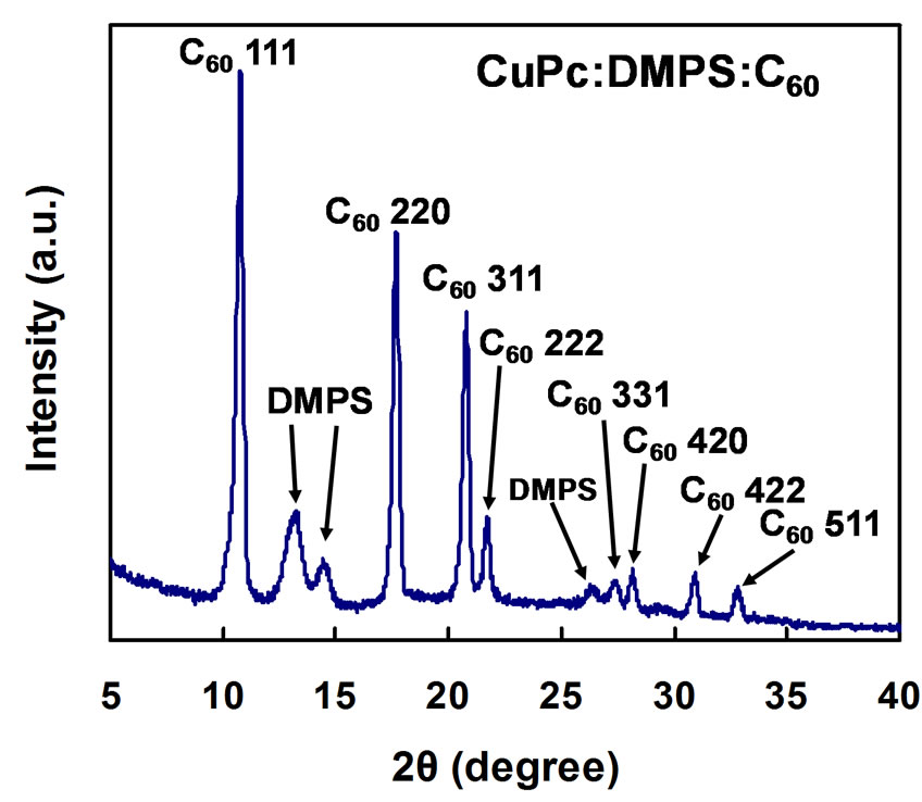
X-ray diffraction patterns of CuPc:DMPS:C60 and DMPS:C60 thin films were shown in Figures 4(a) and (b), respectively. The diffraction patterns showed several diffraction peaks, which were corresponded to DMPS and C60 [15]. Lattice spacings and crystallite sizes of DMPS and C60 in thin films of CuPc:DMPS:C60 and DMPS:C60 are listed in Tables 2(a) and (b), respectively. The crystallite sizes were estimated using Scherrer’s formula of D = 0.9λ/βcosθ. Where λ, β and θ represent
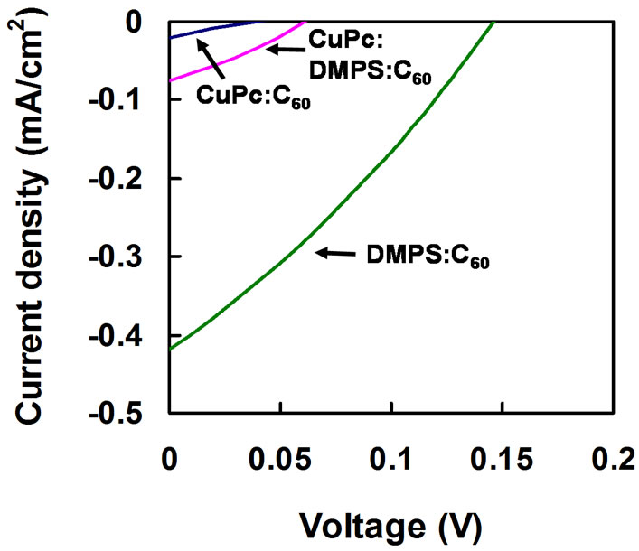
Figure 2. J-V characteristics of CuPc:C60, CuPc:DMPS:C60 and DMPS:C60 bulk heterojunction solar cells.
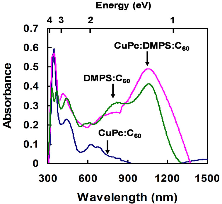
Figure 3. Optical absorption of bulk heterojunction solar cells.
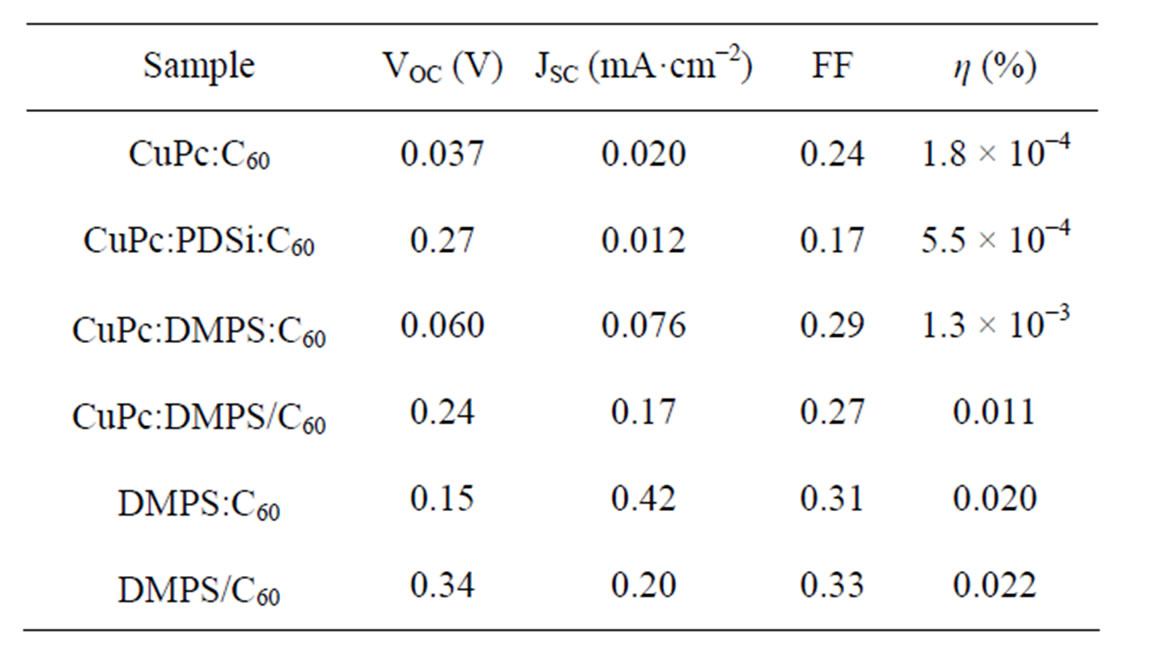
Table 1. Measured parameters of the solar cells.

Table 2. Lattice spacings and crystallite sizes of DMPS and C60 in (a) CuPc:DMPS:C60 and (b) DMPS:C60 thin films. Measured parameters of the solar cells.
the wavelength of the X-ray source, the full width at half maximum and the Bragg angle, respectively [16]. Although the peak positions and lattice spacings are similar, the crystallite sizes were different from one another as shown in Figure 4 and Table 2.
A TEM image and electron diffraction pattern of the DMPS:C60 composite film are shown in Figures 5(a) and (b), respectively. In Figure 5(a), many nanoparticles consisting of a Si element in the C60 matrix were observed. The electron diffraction pattern of Figure 5(b) showed many diffraction spots and Debye-Scherrer rings, which indicated microcrystalline structures of C60 and
 (a)
(a)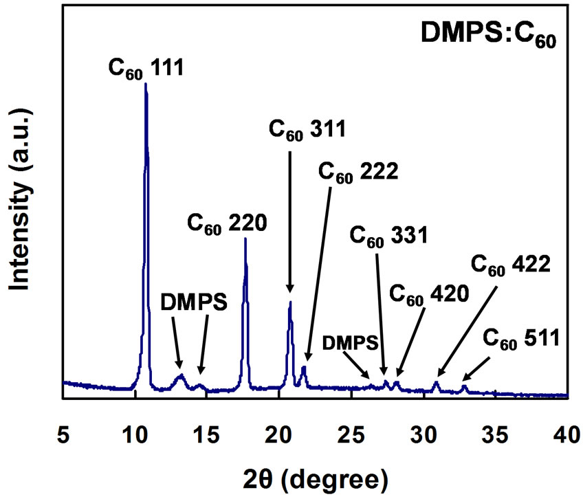 (b)
(b)
Figure 4. XRD patterns of (a) CuPc:DMPS:C60 and (b) DMPS:C60 thin films.
DMPS.
An energy level diagram of CuPc:DMPS:C60 solar cells was summarized as shown in Figure 6. Previously reported values [6,10,17-20] were used for the energy levels of the figures by adjusting to the present work. Electronic charge-transfer separation was caused by light irradiation from the ITO substrate side. Electrons are transported to an Al electrode, and holes are transported to an ITO substrate. It has been reported that VOC is nearly proportional to the band gap of the semiconductors, and control of the energy levels is important to increase efficiency [21].
Polysilane/C60-based solar cells were fabricated by a spin-coating method without vacuum evaporation in the present work. The heterojunction structures were also prepared only by spin-coating. In the Table 1, DMPS/C60 structure yielded the highest efficiency, compared to the other structures. It would be due to a mixture of pand nlayers formed by spin-coating. The photoelectron conversion region in the DMPS/C60 solar cells would be larger than those of the ordinary heterojunction structures, which results in the improvement of conversion efficiency.
 (a)
(a)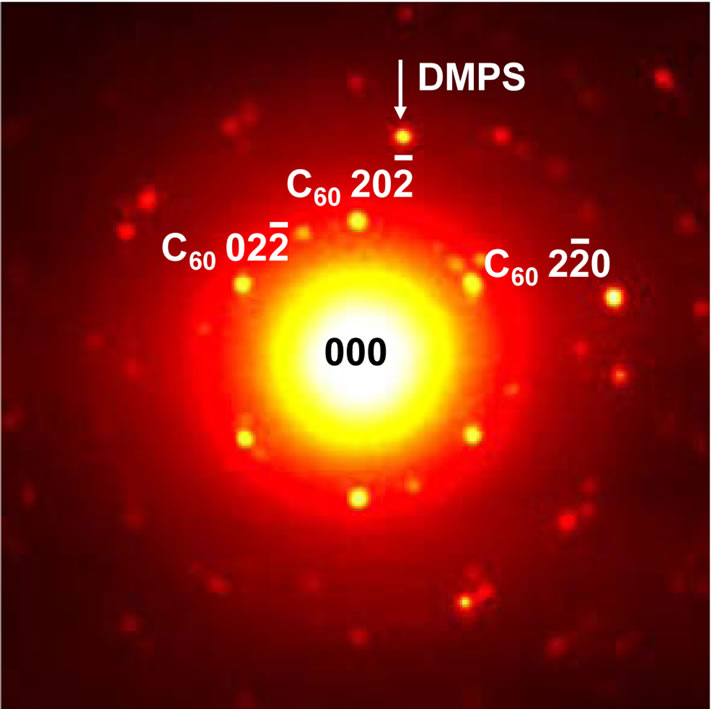 (b)
(b)
Figure 5. (a) TEM image and (b) electron diffraction pattern of DMPS:C60 structure.
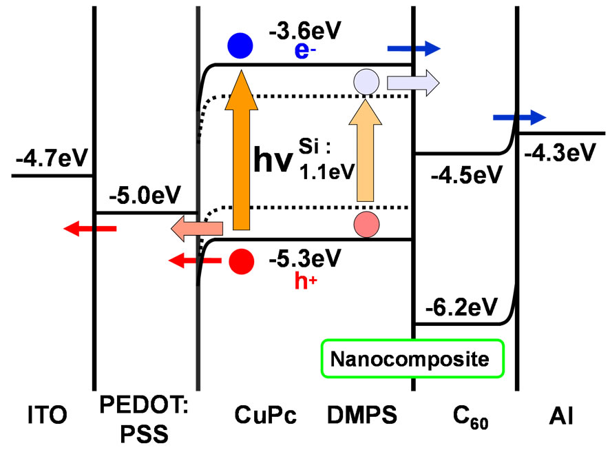
Figure 6. Energy level diagram of CuPc:DMPS:C60 solar cells.
As a factor of the low efficiency, carrier recombination would be a main cause. The defects produced by inadequate crystalline at the p-n interface would cause carrier recombination. Optimization of the microstructures would increase the efficiency of solar cells, which was expected by improving charge separation and the electronic charge transportation [22,23]. There might be carrier recombination of electrons and holes at the rear surface of n-type electrode (ITO). Energy conversion efficiency could be improved by addition of exciton-diffusion blocking layer such as BCP or PTCDA to inhibit carrier recombination at the contact surfaces [24,25].
4. Conclusion
Polysilane/C60-based solar cells were produced and characterized. A device based on the DMPS/C60 structure provided η of 0.022%, FF of 0.33, JSC of 0.20 mA/cm2 and VOC of 0.34 V, which was better than those of other devices in the present work. Microstructures of the solar cells were investigated by using XRD and TEM. The carrier transport mechanism was discussed by the energy level diagram using the experimental results.
REFERENCES
- L. J. A. Koster, V. D. Mihailetchi and P. W. M. Blom, “Ultimate Efficiency of Polymer/Fullerene Bulk Heterojunction Solar Cells,” Applied Physics Letters, Vol. 88, No. 9, 2006, Article ID: 093511. doi:10.1063/1.2181635
- N. S. Sariciftci, L. Smilowitz, A. J. Heeger and F. Wudl, “Photoinduced Electron Transfer from a Conducting Polymer to Buckminsterfullerene,” Science, Vol. 258, No. 5087, 1992, pp. 1474-1476. doi:10.1126/science.258.5087.1474
- T. Oku, T. Noma, A. Suzuki, K. Kikuchi and S. Kikuchi, “Fabrication and Characterization of Fullerene/Porphyrin Bulk Heterojunction Solar Cells,” Journal of Physics and Chemistry of Solids, Vol. 71, No. 4, 2010, pp. 551-555. doi:10.1016/j.jpcs.2009.12.034
- W. Ma, C. Yang, X. Gong, K. Lee and A. J. Heeger, “Thermally Stable, Efficient Polymer Solar Cells with Nanoscale Control of the Interpenetrating Network Morphology,” Advanced Functional Materials, Vol. 15, No. 10, 2005, pp. 1617-1622. doi:10.1002/adfm.200500211
- M. Granström, K. Petritsch, A. C. Arias, A. Lux, M. R. Andersson and R. H. Friend, “Laminated Fabrication of Polymeric Photovoltaic Diodes,” Nature, Vol. 395, No. 6699, 1998, pp. 257-260. doi:10.1038/26183
- T. Oku, A. Takeda, A. Nagata, T. Noma, A. Suzuki and K. Kikuchi, “Fabrication and Characterization of FullereneBased Bulk Heterojunction Solar Cells with Porphyrin, CuInS2, Diamond and Exciton-Diffusion Blocking Layer,” Energies, Vol. 3, No. 4, 2010, pp. 671-685. doi:10.3390/en3040671
- G. Yu and A. J. Heeger, “Charge Separation and Photovoltaic Conversion in Polymer Composites with Internal Donor/Acceptor Heterojunctions,” Journal of Applied Physics, Vol. 78, No. 7, 1995, pp. 4510-4515. doi:10.10631/1.359792
- F. Padinger, R. S. Rittberger and N. S. Sariciftci, “Effects of Postproduction Treatment on Plastic Solar Cells,” Advanced Functional Materials, Vol. 13, No. 1, 2003, pp. 85-88. doi:10.1002/adfm.200390011
- Y. Hayashi, I. Yamada, S. Takagi, A. Takasu, T. Soga and T. Jimbo, “Influence of Structure and C60 Composition on Properties of Blends and Bilayers of Organic Donor-Acceptor Polymer/C60 Photovoltaic Devices,” Japanese Journal of Applied Physics, Vol. 44, No. 3, 2005, pp. 1296-1300. doi:10.1143/JJAP.44.1296
- T. Oku, N. Kakuta, A. Kawashima, K. Nomura, R. Motoyoshi, A. Suzuki, K. Kikuchi and G. Kinoshita, “Formation and Characterization of Bulk Hetero-Junction Solar Cells Using C60 and Perylene,” Materials Transactions, Vol. 49, No. 11, 2008, pp. 2457-2460. doi:10.2320/matertrans.MB200807
- M. A. Abkowitz, “Electronic Transport in Polymers,” Philosophical Magazine Part B, Vol. 65, No. 4, 1992, pp. 817-829. doi:10.1080/13642819208204922
- F. Kajzar, J. Messier and C. Rosilio, “Nonlinear Optical Properties of Thin Films of Polysilane,” Journal of Applied Physics, Vol. 60, No. 9, 1986, pp. 3040-3044. doi:10.1063/1.337759
- C. H. Lee, G. Yu, N. S. Sariciftci, D. Moses, K. Pakbaz, C. Zhang, A. J. Heeger and F. Wudl, “Sensitization of the Photoconductivity of Conducting Polymers by C60: Photoinduced Electron Transfer,” Physical Review B, Vol. 48, No. 20, 1993, pp. 15425-15433. doi:10.1103/PhysRevB.48.15425
- J. Lee, C. Seoul, J. Park and J. H. Youk, “Fullerene/ Poly(Methylphenylsilane) (PMPS) Organic Photovoltaic Cells,” Synthetic Metals, Vol. 145, No. 1, 2004, pp. 11-14. doi:10.1016/j.synthmet.2004.04.022
- J. Feng, J. Han and X. Zhao, “Synthesis of CuInS2 Quantum Dots on TiO2 Porous Films by Solvothermal Method for Absorption Layer of Solar Cells,” Progress in Organic Coatings, Vol. 64, No. 2-3, 2009, pp. 268-273. doi:10.1016/j.porgcoat.2008.08.022
- N. G. Park, M. G. Kang, K. S. Ryu, K. M. Kim and S. H. Chang, “Photovoltaic Characteristics of Dye-Sensitized Surface-Modified Nanocrystalline SnO2 Solar Cells,” Journal of Photochemistry and Photobiology A: Chemistry, Vol. 161, No. 2-3, 2004, pp. 105-110. doi:10.1016/S1010-6030(03)00280-6
- C. W. Chu, V. Shrotriya, G. Li and Y. Yanga, “Tuning Acceptor Energy Level for Efficient Charge Collection in Copper-Phthalocyanine-Based Organic Solar Cells,” Applied Physics Letters, Vol. 88, No. 26, 2006, pp. 153504- 153506. doi:10.1063/1.2194207
- L. Lozzi, S. Santucci and S. La Rosa, “Photoemission Investigation on Copper Phthalocyanine: Fullerene Blend Film,” Applied Physics Letters, Vol. 88, No. 13, 2006, pp. 133505-133507. doi:10.1063/1.2186742
- T. Osasa, S. Yamamoto, Y. Iwasaki and M. Matsumura, “Photocarrier Generation in Organic Thin-Film Solar Cells with an Organic Heterojunction,” Solar Energy Materials and Solar Cells, Vol. 90, No. 10, 2006, pp. 1519-1526. doi:10.1016/j.solmat.2005.10.016
- Y. Terao, H. Sasabe and C. Adachi, “Correlation of Hole Mobility, Exciton Diffusion Length, and Solar Cell Characteristics in Phthalocyanine/Fullerene Organic Solar Cells,” Applied Physics Letters, Vol. 90, No. 10, 2007, pp. 103515-103517. doi:10.1063/1.2711525
- M. A. Green, K. Emery, D. L. King, Y. Hishikawa and W. Warta, “Solar Cell Efficiency Tables (Version 28),” Progress in Photovoltaics: Research and Applications, Vol. 14, No. 5, 2006, pp. 455-461. doi:10.1002/pip.720
- J. Xue, B. P. Rand, S. Uchida and S. R. Forrest, “A Hybrid Planar-Mixed Molecular Heterojunction Photovoltaic Cell,” Advanced Materials, Vol. 17, No. 1, 2005, pp. 66- 71. doi:10.1002/adma.200400617
- P. Sullivan, S. Heutz, S. M. Schultes and T. S. Jones, “Influence of Codeposition on the Performance of CuPcC60 Heterojunction Photovoltaic Devices,” Applied Physics Letters, Vol. 84, No. 7, 2004, pp. 1210-1212. doi:10.1063/1.1643549
- B. P. Rand, J. Genoe, P. Heremans and J. Poortmans, “Solar Cells Utilizing Small Molecular Weight Organic Semiconductors,” Progress in Photovoltaics: Research and Applications, Vol. 15, No. 8, 2007, pp. 659-676. doi:10.1002/pip.788
- V. Tripathi, D. Datta, G. S. Samal, A. Awasthi and S. Kumar, “Role of Exciton Blocking Layers in Improving Efficiency of Copper Phthalocyanine Based Organic Solar Cells,” Journal of Non-Crystalline Solids, Vol. 354, No. 19-25, 2008, pp. 2901-2904. doi:10.1016/j.jnoncrysol.2007.10.098
NOTES
*Corresponding author.