Circuits and Systems
Vol. 3 No. 2 (2012) , Article ID: 18544 , 7 pages DOI:10.4236/cs.2012.32024
Transformerless Battery Charger by Using Constant Current/Constant Voltage Controller
Department of Electrical and Electronics Engineering, Eastern Mediterranean University, Famagusta, North Cyprus
Email: falahalzobe@yahoo.com
Received March 4, 2012; revised April 3, 2012; accepted April 10, 2012
Keywords: Battery Charger; Flyback; Constant Currant; Constant Voltage; Snubber; Efficiency
ABSTRACT
The Battery Charger Specification presents solution for rechargeable batteries used in portable electronic equipment such as laptop computer systems, cellular telephones and video cameras and the demands for low cost battery chargers are rising these days without give attention for the performance. The goal of the paper was combining high efficiency and versatility with low-cost design and this paper includes the design of the snubber cell, and the components of the current/voltage control charge method. This charger applies a relatively constant current and constant voltage to the battery indefinitely regardless of the AC input rang voltage all the equations described in this paper. The design of prototype converter is verified through an experimental result.
1. Introduction
The main function of any battery charger is to cause current to flow back into a battery in the opposite direction from which current flowed during discharge. A battery on charge is not a fixed or static load. It has a voltage of its own and is connected to the charger so that the two voltages oppose each other. Thus, the current that flows is the result of the difference between the voltages of the charger and the battery and a function of the low ohmic resistance of the battery. The voltage of the battery itself rises during the charge, further opposing the flow of current as the charge progresses. The basic requirements of a charger as they relate to the battery are a safe value of charging current throughout the entire cycle, protection against conditions that would result in overcharge, and accurate termination of the charge when complete or reduction of the current to a level which provides a safe charge maintenance value. The desired characteristics of a charger as they relate to the user are Maximum reliability, Automatic operation to the degree practical in the application, Simplicity in design and construction, Good efficiency and power factor, Ease of operation, Reasonable cost and rapid charging.
Battery chargers are designed typically around two modes of operation, namely, constant-voltage charging and constant-current charging. The former utilizes a constant voltage source and an equivalent series resistance to control the amount of current that flows into the battery. As soon as the battery voltage is raised to the voltage sources, the converter must limit its current to prevent excessive dissipation. The latter, moreover, keeps the charging current constant until the battery voltage reaches a designated value [1].
Tiny switch reduces total component count, design size, weight and, at the same time increases efficiency when compared to MOSFET or RCC switch, Figure 1 shows the schematic of the basic battery charger, which also serves as the reference circuit for the design proposes.
2. Proposed Battery Charger Topology
A charger drive circuit that consists of a flyback DC-DC converter with a snubber cell and a constant output current and voltage control as a driver for battery charger is proposed. With this drive circuit, the charger system becomes small size, and has a higher efficiency especially. The configuration for the circuit to charge battery by constant current and constant potential method is shown in Figure 1, where NP and NS winding is a high-frequency transformer, CDC is the input filter capacitor, CP is the output filter capacitor, VDC is the DC input voltage generated by rectifying AC voltage using a bridge rectifier diode, Vo is the output voltage, Io is the output current, DR is a rectifier diode and U1 is a power management IC with a MOSFET incorporated in it connected to a photoelectrical coupler used for photo-electronic isolation. The proposed constant output current and voltage circuit is based on negative-feedback-control theory.
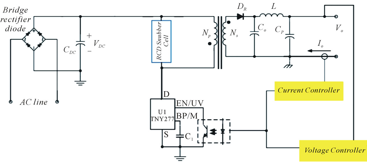
Figure 1. The basic battery charger circuit.
High-frequency transformer is used to transfer energy from input-end to output-end. During the “ON” period for the integrated MOSFET, transformer stores energy in its primary winding and the output current is supplied from the output filter capacity CP only. When the MOSFET Turns “OFF”, the energy stored in the power transformer is transferred to the battery load and to CP as it replaces the charge it lost when it was alone delivering load current. Current controller and voltage controller generates a control signals by comparing the detected voltage with a predetermined reference voltage. U1 regulates the “ON/OFF” time of the integrated MOSFET according to the corresponding control signals, providing a constant output current and constant output voltage with high efficiency converting to the battery at last.
2.1. Power Management IC
A piece of power management IC-TNY277, a member of TinySwitch-III family produced by Power Integrations Inc., is used in the drive circuit. TNY277 incorporates a high-voltage power MOSFET with a power supply controller in one device, using an “ON/OFF” control scheme and offers a design flexible solution with a low system cost and extended power capability. The pin configuretion of TNY277 is shown in Figure 1, where D pin is the power MOSFET drain connection, providing internal operating current for both start-up and steady-state operation and S pin is internally connected to the output MOSFET source for high voltage power return and control circuit common. EN/UV pin has dual functions: enable input and line under-voltage sense. During normal operation, switching of the power MOSFET is controlled by this pin [2].
2.2. RCD Snubber Cell Selection
When the power MOSFET is turned off, there is a high voltage spike on the drain due to the transformer leakage inductance. This excessive voltage on the MOSFET may lead to an avalanche breakdown and eventually failure of the Tiny switch. Therefore, it is necessary to use an additional network to clamp the voltage. The RCD snubber circuit and MOSFET drain voltage waveform are shown in Figures 2 and 3, respectively. The RCD snubber network absorbs the current in the leakage inductance by turning on the snubber diode Dsn once the MOSFET drain voltage exceeds the voltage of node X as depicted in Figure 2. In the analysis of snubber network, it is assumed that the snubber capacitor is large enough that its voltage does not change significantly during one switching cycle. The snubber capacitor used should be ceramic or a material that offers low ESR. Electrolytic or tantalum capacitors are unacceptable due to these reasons [3-5].
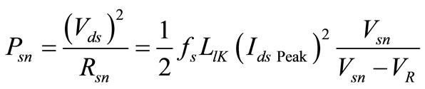
The first step in designing the snubber circuit is to determine the snubber capacitor voltage at the minimum input voltage and full load condition (Vsn). Once Vsn is determined, the power dissipated in the snubber network at the minimum input voltage and full load condition is obtained as
 (1)
(1)
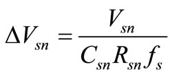
where Ids peak is the maximum peak current through the TNY277 at the minimum input voltage condition, fs is the TNY277 switching frequency, LlK is the leakage in-ductance, Vsn is the snubber capacitor voltage at the minimum input voltage and full load condition, VR is the reflected output voltage and Rsn is the snubber resistor. Vsn Should be larger than VR and it is typical to set Vsn to be 2.5 times VR. Too small a Vsn results in a severe loss in the snubber network as shown in Equation (1). The leakage inductance is measured at the switching frequency on the primary winding with all other windings shorted. Then, the snubber resistor with proper rated wattage should be chosen based on the power loss. The maximum ripple of the snubber capacitor voltage is obtained as
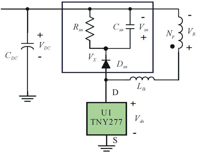
Figure 2. RCD snubber circuit.

Figure 3. MOSFET drain voltage and snubber capacitor voltage.
 (2)
(2)
where fs is the TNY277 switching frequency. The snubber capacitor voltage (Vsn) of Equation (7) is for the minimum input voltage and full load condition, When the converter is designed to operate in CCM under this condition, the peak drain current together with the snubber capacitor voltage decrease as the input voltage increases as shown in Figure 3. The peak drain current at the maximum input voltage and full load condition (Ids Peak) is obtained as
 (3)
(3)
where the maximum input power Pin, is given by
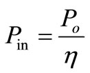 (4)
(4)
where Po is the output power and the η is the circuit efficiency.
And the transformer primary side inductance LP is given by
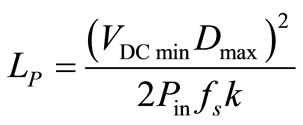 (5)
(5)
where k is the is the ripple factor in full load and minimum input voltage condition and VDC min is the minimum DC link voltage and the maximum duty cycle ratio Dmax is given by
 (6)
(6)
the snubber capacitor voltage under maximum input voltage and full load condition is obtained as
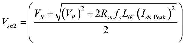 (7)
(7)
where fs is the TNY277 switch frequency, LlK is the primary side leakage inductance, VR is the reflected output voltage and Rsn is the snubber resistor.
From Equation (7), the maximum voltage stress on the internal MOSFET is given by
 (8)
(8)
where is maximum DC link voltage VDC max given by
 (9)
(9)
in this section the snubber cell elements selected successfully to improve the efficiency and performance of the proposed charger.
2.3. Analysis for the Constant-Output-Current and Constant-Output Voltage Circuit
In general, a battery charger employs constant current (CC)/constant voltage (CV) control circuit for an optimal charge of a battery. Figure 4 shown a constant current (CC)/constant voltage (CV) circuit based on the flyback converter is proposed in this paper, a simple, low cost circuit using a comparator (U3) and shunt regulator (U4), being validated with a parametric detailed analysis provided in this section.
DC input voltage VDC is generated by rectifying AC input voltage VAC using a bridge rectifier, and its maximum VDC max is specified in Equation (9).
Assume that the switching frequency and the “ON” period for the power MOSFET are fs and ton, respectively. Then duty ratio D is defined according to the following equation:
 (10)
(10)
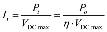
The input power Pi for the drive circuit is calculated by Equation (4) where Po is the output power and the η is the circuit efficiency. Thus the average primary current Ii is represented as follows:
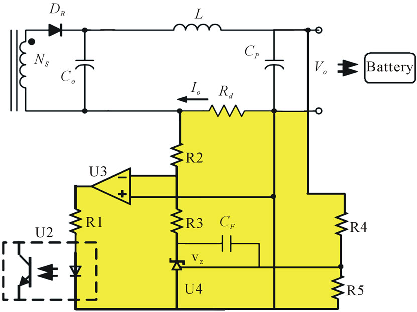
Figure 4. CC/CV control circuit for battery charger.
 (11)
(11)
Assume that the initial current in primary winding is zero ampere.
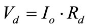
During the MOSFET “ON” period, there is a fixed voltage across primary winding and current in it ramps up linearly. At the end of the “ON” period, the primary current has ramped up to Ip, as shown in Figure 5(a). The relationship between Ii and Ip can be represented as follows:
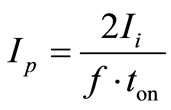 (12)
(12)
The power output of the flyback circuit is determined by the primary inductance LP and the primary current Ip, where LP can be calculated as
 (13)
(13)
When MOSFET turns “OFF”, the current in the magnetizing inductance forces a reversal of polarities on primary winding. Since the current in an inductor cannot change instantaneously, at the instant of turn “OFF”, the primary current transfers to the secondary at an amplitude
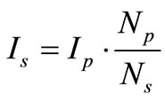 (14)
(14)
where Np, Ns, are the primary and secondary winding turns. During the MOSFET “OFF” period, the secondary current ramps down linearly, shown in Figure 5(b), with an average value calculated as
 (15)
(15)
Finally, from (10)-(14) and by using Equation (4), the circuit output voltage Vo can be represented as the following equation:
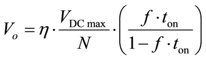 (16)
(16)
where N is the primary/secondary turns ratio. Assume that the reference voltage in Figure 4 is Vref, the voltage detected by Rd is Vd and the voltage across the zener diode U4 is Vz, then the Vr and Vd is given by follwing equations:
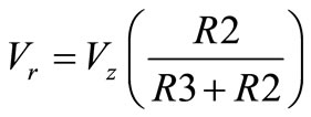 (17)
(17)
 (18)
(18)
when Vd > Vr the photoelectrical coupler (U2) and the MOSFET turns “OFF” to reduce the output current. On the contrary, if Vd < Vr, the photoelectrical coupler leaves off work and the MOSFET turns “ON”, helping increasing the output current.
Constant voltage (CV) control: The voltage divider network of R4 and R5 should be designed to provide Vz to the reference pin of the U4. The relationship between R4 and R5 is given by
 (19)
(19)
where Vo is the output voltage. By Assuming R4 it is easily to obtained R5.
The feedback capacitor (CF) introduces an integrator for CV control. To guarantee stable operation, CF of 470 nF is chosen.
R1 should be designed to provide proper operating current for the shunt regulator (U4) and to guarantee the full swing of the feedback voltage for the TINY 277 Switch.
Finally a snubber cell and constant output current and constant output voltage elements are obtained thus the final scheme of the proposed fly back converter is shown in Figure 6.
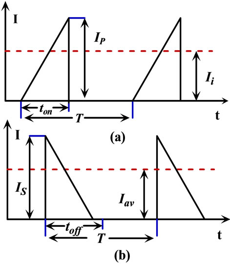
Figure 5. Current waveform in primary winding (a) and (b) secondary winding.
Figure 6. The final scheme of the proposed fly back converter.
3. Experimental Result of Proposed Charger
In order to show the validity of the proposed battery charger presented in this paper, the fly back converter with snubber cell and constant current/constant voltage controller has been built and fabricated with an input range of 85 - 256 AC voltage and the output of 5 V/1 A with 94% efficiency. All the circuit elements values and part number based on Figure 6 are given in Table 1 in Appendix.
Under a constant input of 85 V AC the output voltage vs the output currant is shown in Figure 7 and Figure 8 shows the TNY277 drain voltage Vds and drain current Ids waveforms under a constant input of 85 V AC.
Under an input range of 85 - 265 V AC the circuit output voltage approximately 5 V and the output current approximately 1 A as shown in Figures 9 and 10 respectively also the proposed circuit efficiency according the input AC voltage range is clearly shown in Figure 11.
4. Conclusion
A constant output current and constant output voltage and snubber circuit based on the flyback converter is investigated and a circuit prototype with an output of 5 V/1 A is designed and fabricated the experiments results suggest that the proposed driving method has a high accuracy, good stability and high efficiency. The simulations and experimental results have proven good performances and verify the feasibility of the proposed driving method, and it’s most effective under different
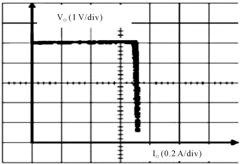
Figure 7. Output voltage vs output current.

Figure 8. Waveforms of drain current and voltage at 85 AC voltage at full load condition.
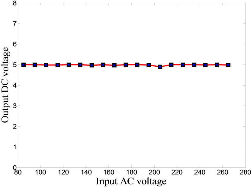
Figure 9. Output voltage vs input AC voltage.
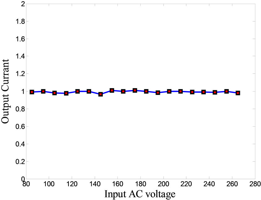
Figure 10. Output current vs input AC voltage.
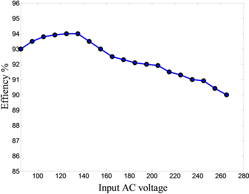
Figure 11. The proposed circuit efficiency according the input AC voltage range.
conditions of industrial applications.
5. Acknowledgements
I would like to express my sincere gratitude to Prof. Dr. Osman Kukrer for his invaluable help and support all over this work.
REFERENCES
- N. K. Poon, B. M. H. Pong and C. K. Tse, “A Constant-Power Battery Charger with Inherent Soft Switching and Power Factor Correction,” IEEE Transaction on Power Electronics, Vol. 18, No. 6, 2003, pp. 1262-4269. doi:10.1109/TPEL.2003.818823
- T. Liu, S. Wang, S. Song and Y. Ai, “Research on High Efficiency Driving Technology for High Power LED Lighting,” Asia-Pacific of Power and Energy Engineering Conference, Chengdu, 28-31 March 2010, pp. 1-4.
- P. C. Todd, “Snubber Circuits: Theory, Design and Applications,” Texas Instrument, Dallas, 2001.
- S. J. Finney, B. W. Williams and T. C. Green “RCD Snubber Revisited,” IEEE Transaction on Industry Application, Vol. 32, No. 1, 1996, pp. 155-160.
- S. Y. R. Hui and H. Chung, “Resonant and Soft-Switching Converters,” In: M. H. Rashid, Ed., Power Electronics Handbook, Academic Press, Cambridge, 2000, pp. 271-304.
Appendix
The table bellow shows the elements values and part numbers of the proposed charger.
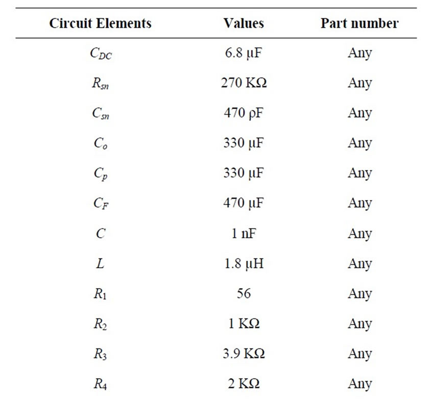
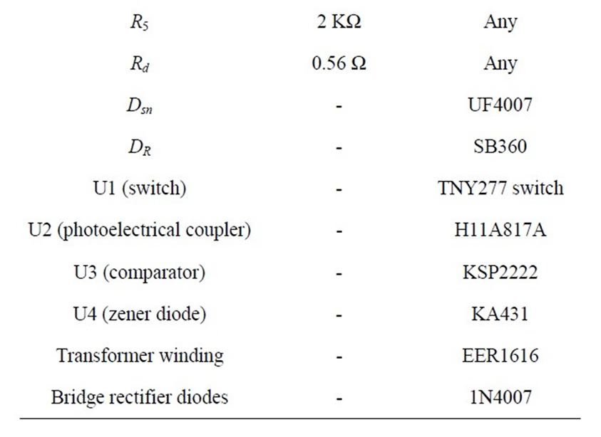
Table 1. The proposed circuit elements value and part numbers.