Circuits and Systems
Vol. 4 No. 2 (2013) , Article ID: 29866 , 9 pages DOI:10.4236/cs.2013.42026
A Modified Approach for CMOS Auto-Zeroed Offset-Stabilized Opamp
Faculty of Electrical and Computer Engineering, University of Tabriz, Tabriz, Iran
Email: A.taghizadeh@tabrizu.ac.ir
Copyright © 2013 Abouzar Taghizadeh et al. This is an open access article distributed under the Creative Commons Attribution License, which permits unrestricted use, distribution, and reproduction in any medium, provided the original work is properly cited.
Received November 7, 2012; revised January 29, 2013; accepted February 6, 2013
Keywords: Auto-Zeroing; Chopping; Offset-Stabilization; Opamp
ABSTRACT
In this paper, a very low-offset continuous time amplifier has been presented. It has the fully differential structure and uses an Auto-zeroed offset stabilization technique. This structure consists of two phases in which the offset value is sampled in the first phase and then subtracted from the signal in the second phase. In order to maintain the continuous time topology, the amplifier uses two paths called main-path and sub-path where the main-path is never disconnected from the signal path and as a result the structure will be continuous time. The amplifier is designed to have a total amount of power dissipation about 3 mW in the standard 0.35 μm CMOS process. Furthermore, the proposed Opamp has an offset value lower than 1 μV at a 2.5 kHz Auto-zeroing frequency, unity gain frequency of 6.14 MHz and phase margin of 78.6˚ with 50 pF loads.
1. Introduction
Low-offset amplifiers are essential components in measurement systems. In many applications such as instrumentation amplifiers, thermocouples and sensors, offset is one of the most important factors that limits the performance of the system. During last few years, there has been a significant increase in the use of CMOS instead bipolar technology which has usually higher offset and 1/f noise. Although the offset of a typical CMOS amplifier is about a few millivolts, still this small value limits its accuracy and dynamic range. The most popular offset cancellation technique in bipolar technology is trimming, which is not desired for CMOS technology because it is an expensive technique and cannot reduce the 1/f noise. Three main classes of dynamic offset-cancellation (DOC) techniques can be found in data books and literature where Auto-zeroing is the first group of them [1]. In this technique, offset is sampled in the first phase and subtracted from the main signal in the next phase. Autozeroing technique is not suitable for continuous time process because the signal path is disconnected from the signal in one of the two phases, unless the ping-pong architecture is used [2,3]. Chopping is the second one of DOC techniques [4,5]. In this technique offset is frequency modulated and removed by a low pass filter which limits the bandwidth of the amplifier and so this technique is not suitable for high bandwidth applications. Another technique in DOC is offset-stabilization which is better than the two previous techniques [6,7]. In this technique offset compensation is achieved by using a sub-path in parallel with a main-path. The sub-path has low value of offset which is reduced using chopping or Auto-zeroing technique. The main advantage of offset-stabilization is that the signal path does not have to be sampled or modulated, thus the whole bandwidth of the main-path is maintained for the amplifier.
2. Offset-Stabilization Technique
Offset-stabilization technique, depending on the method which is applied in the sub-path, is divided into two groups: chopper offset-stabilization and Auto-zeroed offset-stabilization. Each of them has certain advantages and disadvantages. The inherent tradeoffs between two basic topologies are described in [1].
2.1. Chopper Offset-Stabilization
In Figure 1 the block diagram of a chopper offset-stabilization structure is shown. This system uses a chopper amplifier as the auxiliary amplifier in the sub-path. The chopper amplifier consists of chopper CH1, transconductor gm2, chopper CH2 and low pass filter (LPF).
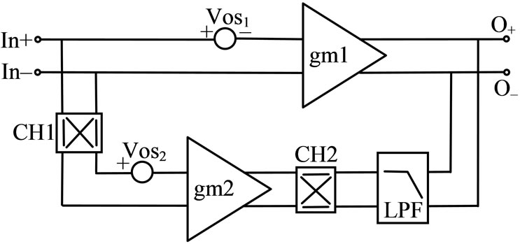
Figure 1. Chopper offset-stabilization structure.
The input signals of the sub-path are modulated with CH1, amplified and demodulated back to the original band. The offset of the transconductor gm2 (Vos2) is modulated only once and transposed to the odd harmonic frequencies of the modulation signal. Thus the LPF can remove it. Hence the low offset sub-path is prepared and an offset compensating current is applied to gm1. At steady state, it can be proved that the residual offset of the system is given by [8]
 (1)
(1)
where the Vos1 is the offset voltage of the amplifier gm1 and A1, A2, A3 are the DC voltage gains of the gm1, gm2 and LPF, respectively. It should be noticed that since the residual offset of sub-path can increase the offset of the system, the implementation of LPF is very important. In [9], the LPF is realized with an integrator and in [10] a switched capacitor filter is used as the LPF.
2.2. Auto-Zeroed Offset-Stabilization
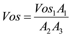
Figure 2(a) shows a system using Auto-zeroed offsetstabilization and the timing of the clock signals for controlling the internal switches of the amplifier is shown in Figure 2(b). According to these signals, two different phases can be considered for this technique. First phase is a sampling phase (φ1) during which the offset voltage of gm2 is sampled and stored on the C1, C2 as a differential voltage. In the next phase (φ2) this stored voltage removes the offset of gm2 and with this low-offset subpath the offset compensating voltage is applied to gm1. In this structure, gm1 as the main amplifier is never disconnected from the signal and as a result the structure will be continuous time [11].
3. Offset and Noise in CMOS Amplifiers
In the differential structure, two sides of circuit mostly assumed perfectly symmetric. Reality, nominally-identical devices suffer from a finite mismatch due to uncertainties in each step of the manufacturing process. One of the results of this asymmetrically is generation of offset voltage. Also threshold voltage (Vth) in MOS devices is a function of the doping levels in the channel and the gate, and these levels vary randomly from one device to
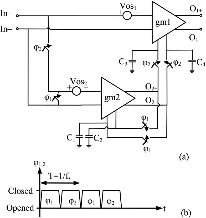
Figure 2. (a) Auto-zeroed offset-stabilization structure; (b) Clock timing signals.
another. The mentioned factor increases of offset voltage [12].
Beside the offset, a typical CMOS amplifier has another non-ideality called input referred noise. For high frequencies the noise spectrum is limited to the thermal noise which is considered as frequency independent or white noise. At low frequencies noise is usually dominated by the flicker noise components. The flicker noise is an inherent noise in the physics of semiconductor devices which is inversely proportional to the frequency and is therefore called 1/f noise. The Frequency at which the 1/f noise is equal to the white noise is called the 1/f noise corner frequency, fc [13]. Low frequency noise is considered as the offset in the DOC techniques and as a result these techniques can remove it. The residual noise of chopper offset-stabilization amplifier is fundamentally lower than that of Auto-zeroed offset-stabilization amplifier. The reason is mainly due to the fact that the Autozeroing topologies suffer from aliasing or folding back of their broadband noise spectrum sampled during their zeroing cycle that increase the overall input-referred noise [7].
It should be noticed that in order to remove all the 1/f noise in both two group of offset-stabilization techniques, the sampling frequency in Auto-zeroing technique and the chopping frequency in the chopping technique are always should be higher than the 1/f noise corner frequency.
4. Proposed OPAMP
Figure 3 shows the proposed OPAMP structure. In this structure, the Auto-zeroed offset stabilization topology which is shown in Figure 2 is used to perform offset cancellation. Furthermore, in order to increase DC gain
Figure 3. proposed OPAMP.
and bandwidth and improve the frequency response, gm3 and gm4 stages are applied which will be discussed latter.
4.1. Offset Cancellation Theory
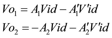
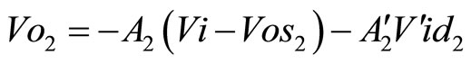
The proposed structure has four internal amplifiers that two of them require two differential inputs. One is used as a primary input and the other as an auxiliary input. Figure 4 shows the structure of this internal amplifier. The output voltage 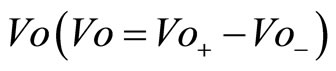 can be expressed as
 (2)
(2)
where A, Vid and  are the DC gain and the differential input voltages of the primary and auxiliary inputs, respectively, whereas the subscript modifiers “1” and “2” denote parameters belonging to the gm1 and gm2, respectively.
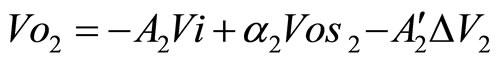
With respect to Figure 2, in the first phase, all φ1 switches are closed and all φ2 switches are opened. Here, the output of gm2 is connected to the auxiliary inputs and the primary inputs are connected together. In this state, the output voltage of gm2 is:
 (3)
(3)
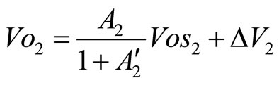
voltage ∆V2 corresponds to the voltage change due to charge injection, sampled noise and leakage current in the desirable differential voltage at C1 and C2. [6].
In the next phase, when the φ2 switches close and φ1 switches open, this Voltage remain on C1, C2 as a differential voltage and essentially corrects the offset of gm2. Hence the output voltage of gm2 is determined as
 (4)
(4)
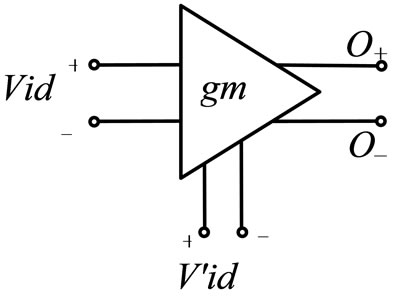
Figure 4. Internal amplifier.
where 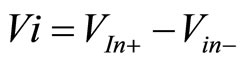 and
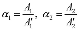
and  is equal to the voltage at the output of the gm2 at the time when φ1 was closed. If the ratio of the open loop DC gains between the primary and auxiliary inputs is defined as
 (5)
(5)
and substituting (4) and (5) into (3), yields
 (6)
(6)
where it has been assumed that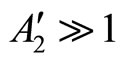 . In this phase, the output voltage of gm1 is given by
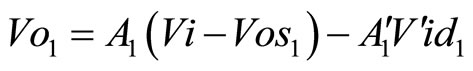 (7)
(7)
here  is equal to Vo2 in (6). Substituting this into (7) results in
 (8)
(8)
By defining VOS(2) as the residual offset voltage during the phase φ2, the output voltage is equal to zero if Vi = VOS(2). Due to the fact that A1 is too small compared to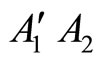 , the first term on the right-hand side of (8) could be approximated as
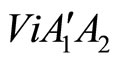 . Imposing the output voltage to zero and solving for Vi = VOS(2) results in
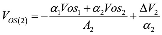 (9)
(9)
At the end of phase φ2 the output voltage of gm1 will change by an amount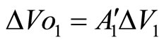 , where the voltage
  similar to
  corresponds to the voltage change due to charge injection, sampled noise and leakage current in the desirable differential voltage at C3 and C4
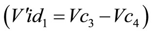 . As a result in this phase, the residual offset voltage in the phase φ2, VOS(2) should be changed by an amount
 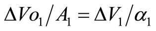 in order to bring the output voltage back to zero again. The resulting residual input-referred offset voltage VOS(1) valid for phase φ1 is therefore slightly different than for phase φ2 and is given by:
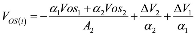 (10)
(10)
Both (9) and (10) show that the residual offset voltage is proportional to the sum of the Vos1 and Vos2 divided by the DC gain of the primary input of gm2. By choosing , nonideal effect terms can be reduced but at the cost of an increase in the first term due to Vos1 and Vos2. In this circuit, with respect to using of differential structure, the non-ideal effect terms contained in
  and
and  are very low and thus
  is considered.
4.2. Circuit Details
The opamp is designed with fully differential structure and uses four gm stages. In This topology, as mentioned, the gm1 and gm2 stages reduce the offset and noise while the DC gain increase and improvement of the frequency response are determined by gm3 and gm4. The main-path is determined by gm1’s primary input, gm3 and gm4 that provide a good DC gain and appropriate unity-gain frequency. As a result the continuous time capability for the system is maintained. In parallel with this path, sub-path which includes the gm2’s primary input, gm1’s auxiliary input, gm3 and gm4, has high DC gain but it is not unity-gain stable while the main-path maintains a first-order roll-off at unity-gain crossover for stability [10].
The equivalent offset voltage of the main-path and sub-path is illustrated by Vos1 and Vos2, respectively, that the typical amount of them is assumed 10 mv. This means that, in order to reduce the offset of the system to 1 µV, the gain of the gm2’s primary input (A2) must be higher than 86 dB or a factor of 20,000.
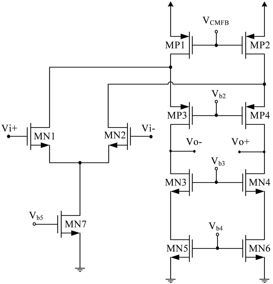
A more detailed circuit diagram of the proposed structure is as follows: the input stage gm1 and the compensated stage gm2 are designed based on folded cascode amplifier with two differential inputs and the system has a class AB output stage that consists of a folded cascode gm3 and a simple class AB output stage gm4 [14]. The circuit that is used as gm3 is shown in Figure 5(a) [15]. The input transistors MN1, MN2 are selected as n-channel because they can operate in the output common mode voltage of the prior stage.
A continuous time common mode feedback (CMFB) circuit is used for gm3 which is shown in Figure 5(b). If Vref equals to the common mode voltage of ,
,  , then the sum of these two pair transistors (MPC3-4 and MPC5-6) drain current is constant [15]. The CMFB will sense the output CM level, compare it with the Vref and return the error to the amplifier’s bias network.
As already mentioned, gm1 and gm2 must have two differential inputs. In the gm1, this aim is realized with two active loads as shown in Figure 6. By selecting the same size and current in both main and auxiliary inputs, the  parameter is nearly equal to one
 . The output common-mode device MPC1 and MPC2 has the roll of CMFB circuit and sets the output common-mode bias voltage.
In order to achieve the low offset voltage,  and
and  is needed to be high
 . For high gain design, two-stage configuration might be an appropriate choice.
 (a)
(a)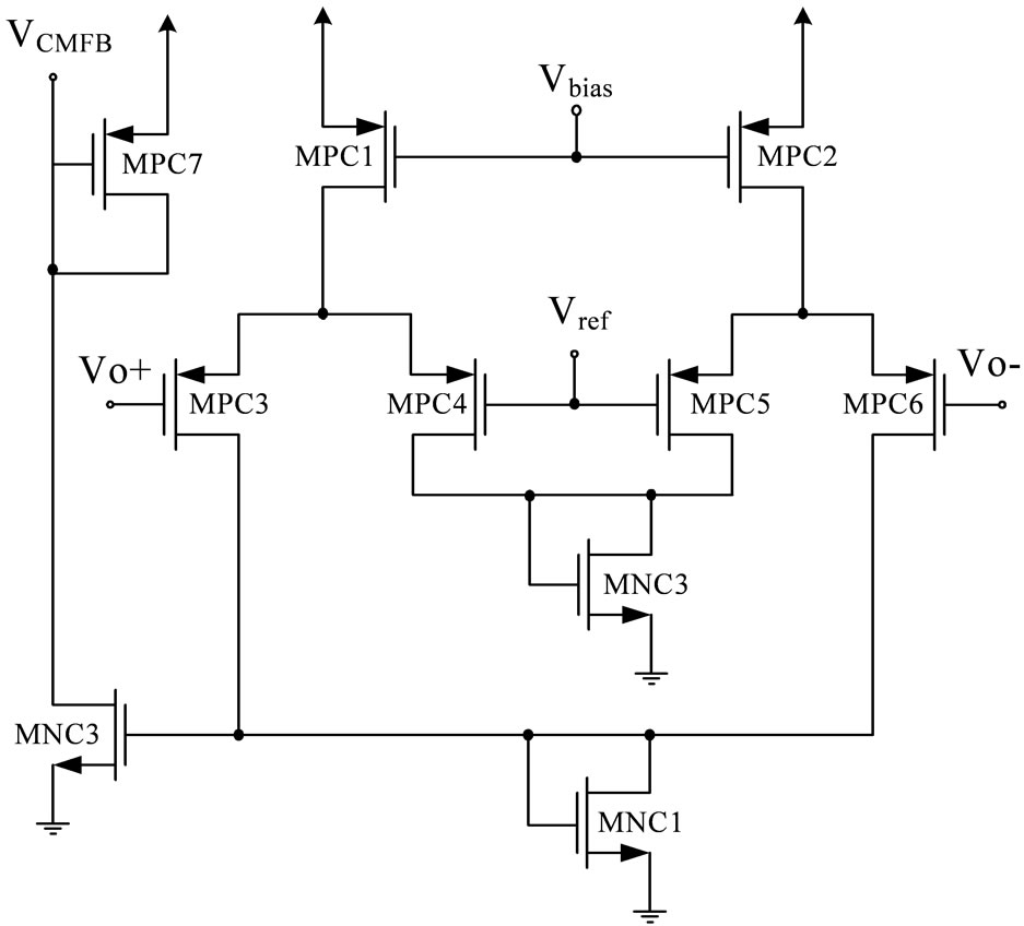 (b)
(b)
Figure 5. (a) Circuit diagram of the gm3 stage; (b) CMFB of gm3.
However, the speed of this configuration is limited. But the single stage opamp with gain boosting technique not only gives high gain but also good bandwidth without any compensation. In this design, a fully differential folded cascode opamp that has four gain boosting circuits is chosen as gm2 as shown in Figure 7" target="_self"> Figure 7.
Furthermore, to achieve higher gain, since the output impedance of p-channel transistor is less than n-channel one, additional cascode transistors, MP6 and MP7 are included. The same CMFB circuit as that of the gm1 is used for setting the output common mode voltage and biasing of MP1 and MP2. To realize the two differential
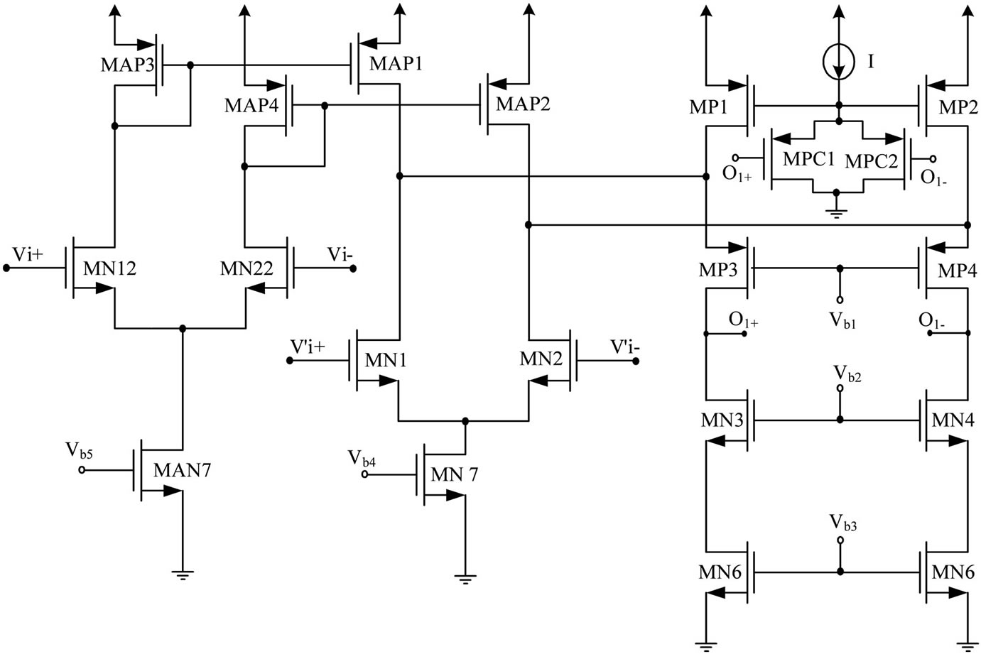
Figure 6. Schematic of gm1 stage including CMFB circuit.
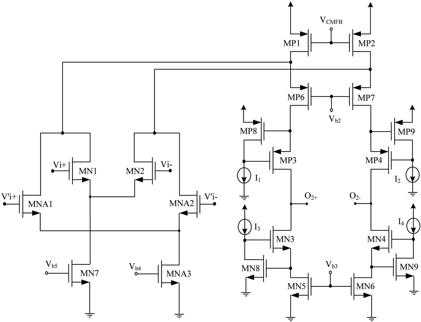
Figure 7. Schematic of gm2 stage.
pair inputs, an additional differential pair MNA1 and MNA2 is connected in parallel with the main input pair MN1 and MN2.
5. Simulation Results
The proposed Auto-zeroed offset-stabilized opamp has been designed and simulated in HSPICE using a 0.35 µm standard CMOS process. The whole circuit consumes about 3 mW from a 3.3 V supply. Each stage of gm1 and gm2 steers nearly 250 µA while each of gm3 and gm4 has nearly 200 µA. As mentioned, to reach better offset cancellation, the sampling frequency should be selected sufficiently higher than the 1/f noise corner frequency which is obtained about 2 kHz for our circuit. Therefore the sampling clock frequency is chosen 2.5 kHz.
In order to keep the offset cancelling voltage during the compensating phase, the hold capacitors C1, C2, C3 and C4 are chosen as 10 pF.
The capacitors Cf1, Cf2 and Cf3, Cf4 are used for frequency miller compensation in two phases’ φ1 and φ2 and were selected 6 pF and 10 pF, respectively. In the phase φ2, as mentioned previously, the sub-path compared to the main-path, has a high DC voltage gain, but it is not unity gain stable. Stability was tested during the design by injecting a small transient current pulse at each internal node and monitoring the voltage response on the node over many clock cycles.
Simulations have been performed on a 50 pF load in both nodes of the outputs. The frequency response of main-path of circuit is shown in Figure 8. As it is shown, the open loop DC gain is around 100 dB, unity gain and phase margin is 6.14 MHz and 78.6˚, respectively.
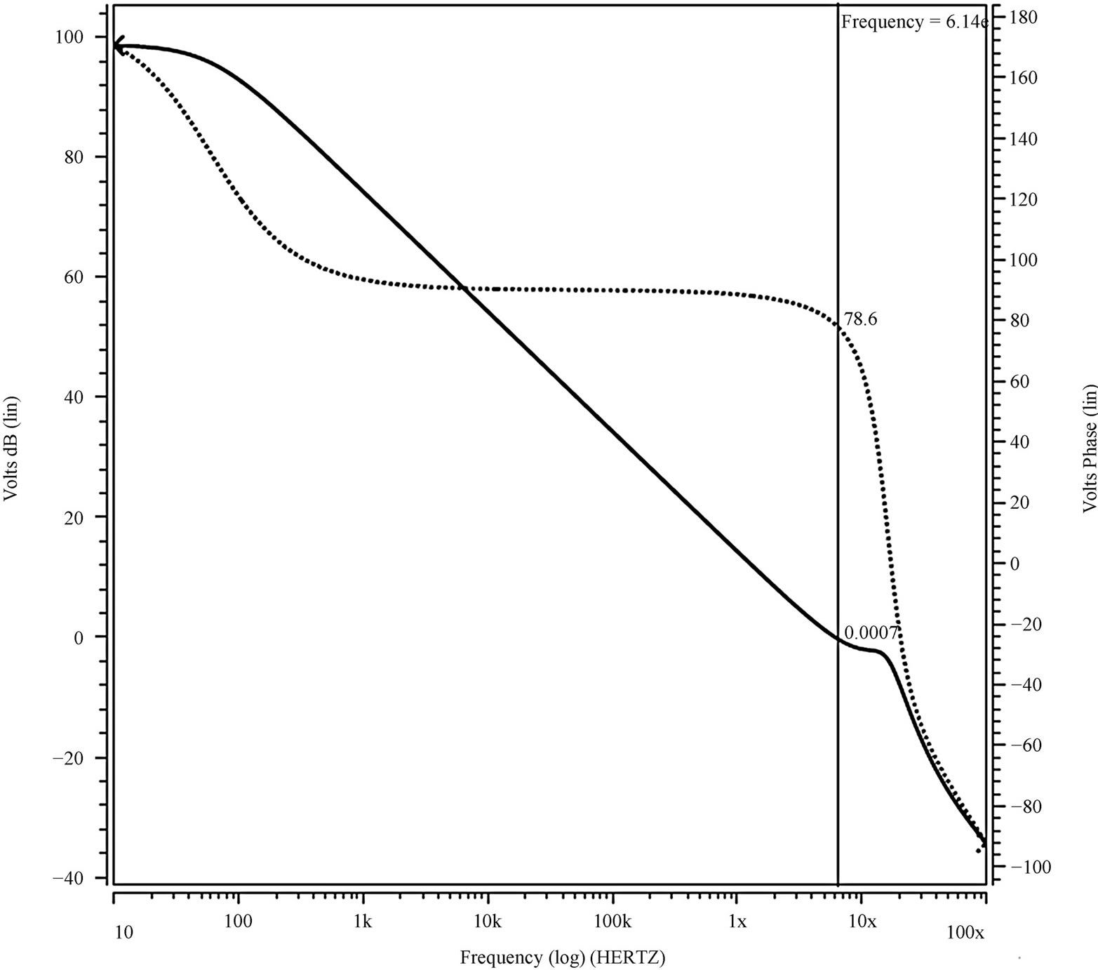
Figure 8. Frequency response of the main-path.
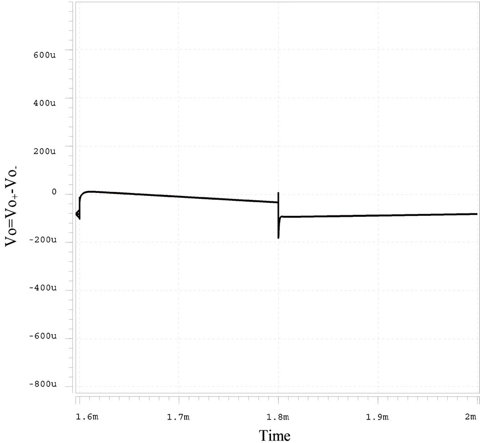
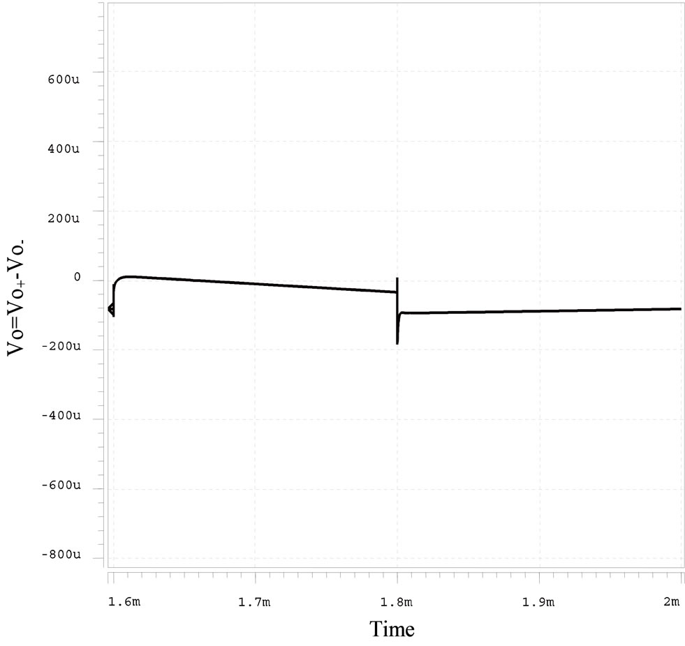
With respect to circuit, If the input voltage is equal to zero (Vin = 0), the equivalent input referred offset voltage can be measured to the dividing the output voltage  by a gain factor of the feedback (Rf/Ri). To demonstrate the offset cancelling of the designed opamp, all of the possible cases of Vos1 and Vos2 were simulated (
 ). Figure 9" target="_self"> Figure 9 shows the simulation results of opamp output voltage (Vo) in four cases of Vos1 and Vos2 as mentioned above. As it is shown, the input referred offset in all cases, is lower than 1 μV.
Furthermore, changes in opamp parameters—specially input referred offset voltage—over process corner and temperature and voltage supply variation has been simulated and the results show variations of less than 10%. Figure 10 shows that the worst state is fast-slow, among the four cases of output voltage slow-slow, fast-fast, slow-fast and fast-slow instances of NMOS and PMOS transistor parameters for the 0.35 µm CMOS process.
Table 1 shows a comparison between present work and two other state of the art designs which are reported in [7,8]. Finally, the low offset and low power characteristics make this design very attractive for use in the instrumentation applications e.g. submicrovolt sensor.
 (a)
(a) (b)
(b) (c)
(c)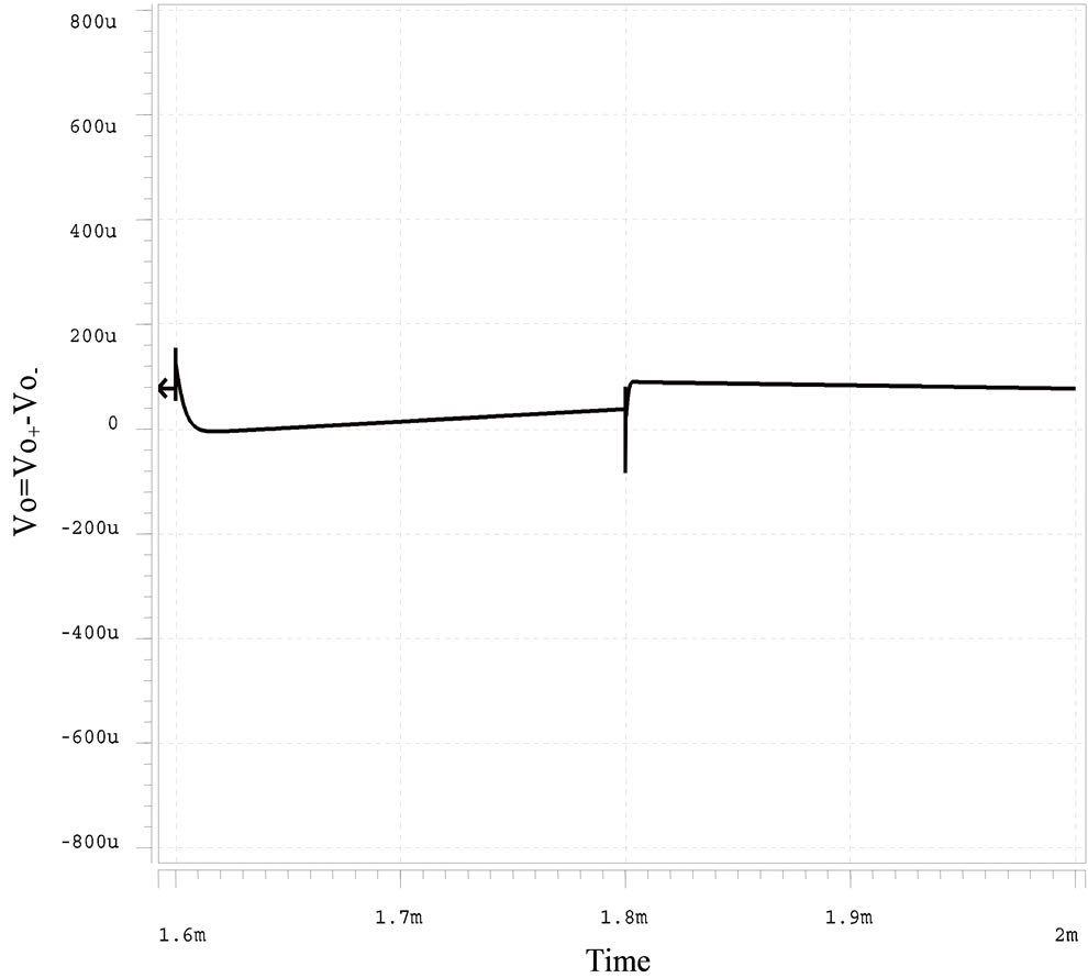 (d)
(d)
Figure 9. Simulation results of the output voltage (Vo) for Vi = 0 (Vi+ − Vi− = 0), Rf/Ri = 100. (a) Vos1 = 10 mV, Vos2 = 10 mV; (b) Vos1 = 10 mV, Vos2 = −10 mV; (c) Vos1 = −10 mV, Vos2 = 10 mV; (d) Vos1 = −10 mV, Vos2 = −10 mV.
 (a)
(a)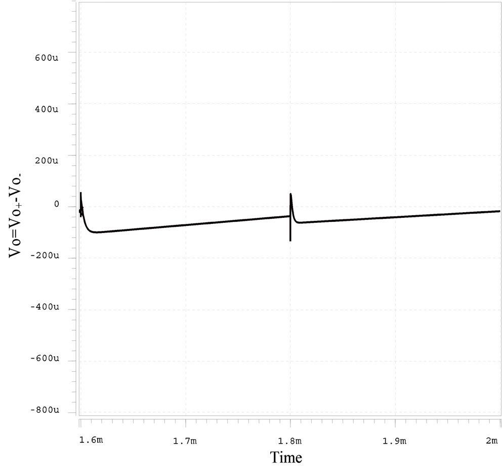 (b)
(b)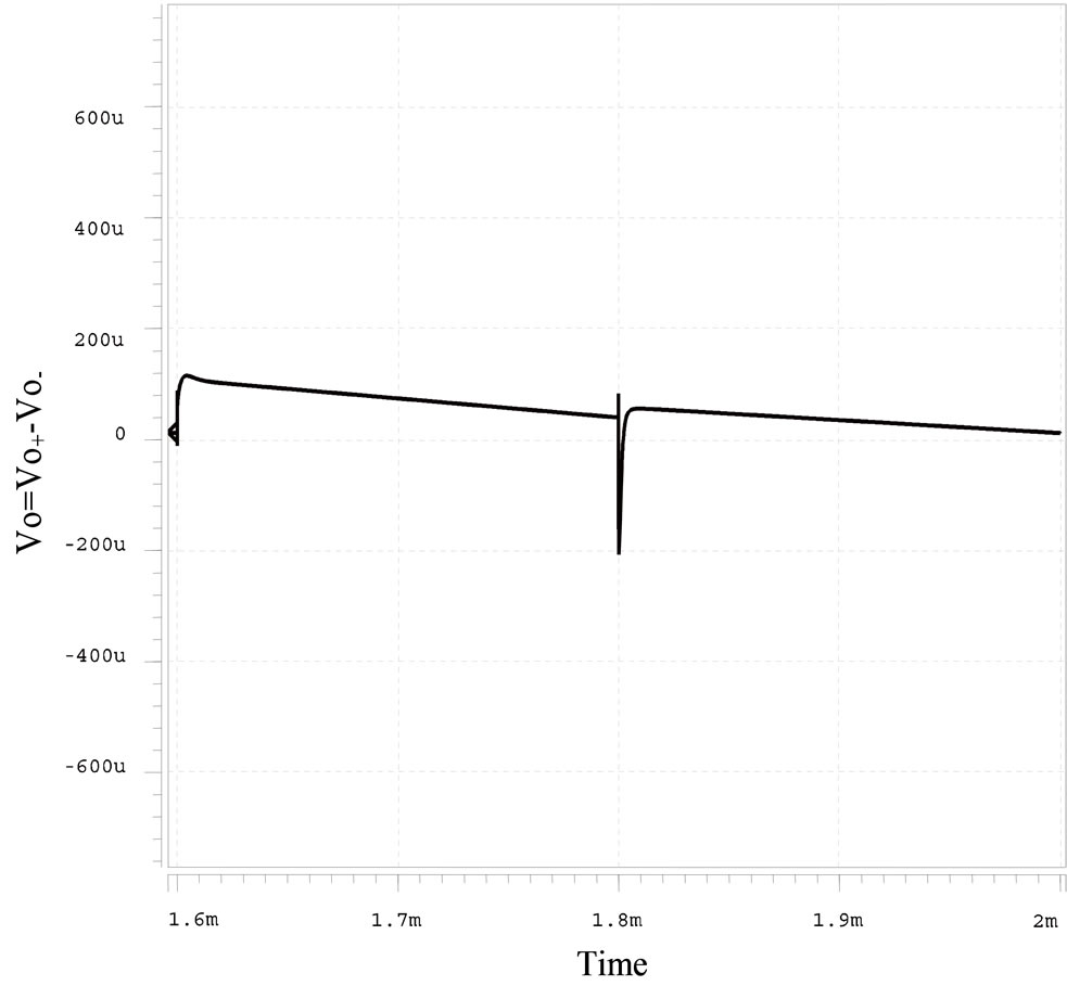 (c)
(c)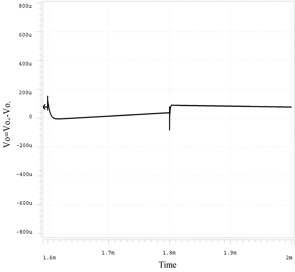 (d)
(d)
Figure 10. Simulation results of the output voltage (Vo) in the FS corner for Vi = 0 (Vi+ − Vi− = 0), Rf/Ri = 100. (a) Vos1 = 10 mV, Vos2 = 10 mV; (b) Vos1 = −10 mV, Vos2 = 10 mV; (c) Vos1 = 10 mV, Vos2 = −10 mV; (d) Vos1 = −10 mV, Vos2 = −10 mV.
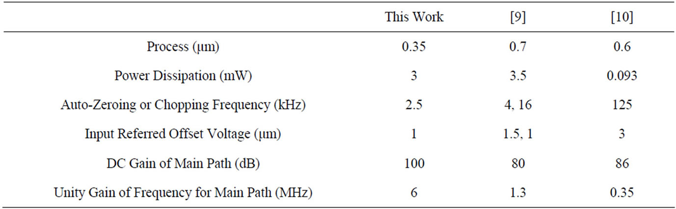
Table 1. Comparison of chopper and auto-zeroed opamps.
6. Conclusion
In this paper, a very low offset, fully differential opamp in the standard 0.35 μm CMOS process is designed based on Auto-zeroed offset stabilized technique. This structure has continuous time topology and its performance is determined by two feedforward paths, in such a way that one of them is used to reduce the offset of the other. When the output capacitor loads are 50 pF, this design exposes a unity gain frequency of 6.14 MHz with a phase margin of 78.6˚ and has an offset value less than 1 μV at 2.5 kHz Auto-zeroing frequency.
REFERENCES
- C. C. Enz and G. C. Temes, “Circuit Techniques for Reducing the Effects of Opamp Imperfections: Autozeroing, Correlated Double Sampling, and Chopper Stabilization,” Proceedings of the IEEE-PIEEE, Vol. 84, No. 11, 1996, pp. 1584-1614. doi:10.1109/5.542410
- C. G. Yu and R. L. Geiger, “An Automatic Offset Compensation Scheme with Ping-Pong Control for CMOS Operational Amplifiers,” IEEE Journal of Solid-State Circuits, Vol. 29, 1994, pp. 601-610.
- M. A. P. Pertijs and W. J. Kindt, “A 140 dB-CMRR Current-Feedback Instrumentation Amplifier Employing PingPong Auto-Zeroing and Chopping,” IEEE Journal of Solid-State Circuits, Vol. 45, No. 10, 2010, pp. 2044-2056. doi:10.1109/JSSC.2010.2060253
- A. Bakker, K. Thiele and J. H. Huijsing, “A CMOS Nested-Chopper Instrumentation Amplifier with 100-nV Offset,” IEEE Journal of Solid-State Circuits, Vol. 35, No. 12, 2000, pp. 1877-1883. doi:10.1109/4.890300
- C. Menolfi and Q. Huang, “A Fully Integrated CMOS Instrumentation Amplifier with Submicrovolt Offset,” IEEE Journal of Solid-State Circuits, Vol. 34, No. 3, 1999, pp. 415-420. doi:10.1109/4.748194
- M. C. W. Coln, “Chopper Stabilization of MOS Operational Amplifiers Using Feed-Forward Techniques,” IEEE Journal of Solid-State Circuits, Vol. SC-16, No. 6, 1981, pp. 745-748. doi:10.1109/JSSC.1981.1051671
- J. F. Witte, J. H. Huijsing and K. A. A. Makinwa, “A Chopper and Auto-Zero Offset-Stabilized CMOS Instrumentation Amplifier,” Symposium on VLSI Circuits Digest of Technical Papers, 2009, pp. 210-211.
- H. Scmicond, “ICL7650S Super Chopper-Stabilized Operational Amplifier,” Linear & Telecom IC’s for Analog Signal Processing Applications Data Book, 1991, pp. 3-526-3-536.
- J. F. Witte, K. A. A. Makinwa and J. H. Huijsing, “A CMOS Chopper Offset-Stabilized Opamp,” IEEE Journal of Solid-State Circuits, Vol. 42, No. 7, 2007, pp. 1529-1537. doi:10.1109/JSSC.2007.899080
- R. Burt and J. Zhang, “A Micropower Chopper-Stabilized Operational Amplifier Using SC Notch Filter with Synchronous Integration inside the Continuous-Time Signal Path,” IEEE Journal of Solid-State Circuits, Vol. 41, No. 12, 2006, pp. 2729-2736. doi:10.1109/JSSC.2006.884195
- I. G. Finvers, J. W. Haslett and F. N. Trofimcnkofl, “A High Temperature Precision Amplifier,” IEEE Journal of Solid-State Circuits, Vol. 30, No. 2, 1995, pp. 120-128. doi:10.1109/4.341738
- B. Razavi, “Design of Analog CMOS Integrated Circuits,” McGraw-Hill, New York, 2000.
- A. T. K. Tang “A 3 μV-Offset Operational Amplifier with 20 nV/√Hz Input Noise PSD at DC Employing Both Chopping and Autozeroing,” IEEE International SolidState Circuits Conference on Digest of Technical Papers, Vol. 1, 2002, pp. 386-387.
- F. S. H. K. Embabi and E. S. Cinencio, “Low Voltage Class AB Buffer with Quiescent Current Control,” Journal of Solid-State Circuits, Vol. 33, No. 6, 1998, pp. 915-920. doi:10.1109/4.678659
- D. A. Johlns and K. Martin, “Analog Integrated Circuit Design,” John Wiley & Sons, Hoboken, 1997.