Circuits and Systems
Vol. 3 No. 3 (2012) , Article ID: 20195 , 6 pages DOI:10.4236/cs.2012.33036
A Novel High CMRR, Low Power and Low Voltage COS with QFG
Electronics Department, Iran University of Science and Technology, Tehran, Iran
Email: arghorbani@elec.iust.ac.ir, aghanaatian@ee.iust.ac.ir
Received June 29, 2011; revised May 9, 2012; accepted May 16, 2012
Keywords: CMRR; QFG; Current Mode; Current Operational Amplifier (COA); COS
ABSTRACT
A novel high CMRR current output stage (COS) with QFG is presented in this paper. A novel common mode feedback (CMFB) is used to reject the common mode signal in order to achieve high CMRR. The common mode signal is omitted by the technique of adding the main signal and its opposite polarity one. 112 dB of CMRR is obtained in 0.35 µm CMOS technology with ±0.75 v supply voltage and only 182 µw power dissipation which shows good improvement compared to the other work in the literature.
1. Introduction
Current operational amplifier (COA) have been used as feasible alternative to traditional voltage amplifier (VOA) in order to use in high accuracy closed loop IC configuration [1-3]. Excellent performance feature of current mode blocks, have become main reason to use current mode signal processing instead of voltage mode. Today’s, it is well known that high speed and accuracy, low level supply, small size and wide band dynamic range could be achieved by taking advantages of the current mode blocks [1-6]. The current-mode output stage (COS) can be used as the end part of COA, moreover, it could be considered as voltage to current convertor (VIC) which is very significant analog block especially in high frequency applications [7-10]. Many important properties of COA like offset and CMRR is determined by COS which shows great value of this block [7,10-13].
Several COS’s have been proposed in literature to improve the parameters like CMRR. [11] fixed the potential at the source of COA transistors by two auxiliary differential amplifier to improve CMRR. But these structures suffer from high power dissipation and high supply voltage. [14] used the same method to achieved high CMRR while it could decrease supply voltages to some extent. [10] used CMFF technique to improve CMRR, but suffer from stability and high supply voltage problem.
The COS’s usually constructed in single input, differential output, however the fully differential structure can improve some properties like CMRR, PSRR [13-16]. In this paper a simple fully differential structure of COS is proposed. The CMFB technique is used to remove the common mode signal in the output of COS to improve CMRR. This novel CMFB provide low voltage, low power and much higher CMRR compared to the others in the literature.
QFG transistors are the improved version of MIFG (Multiple Input Floating Gate) transistors [7]. These circuits achieve LV operation by implementing capacitive voltage dividers at the transistor gate. In QFG transistors, similarly to MIFG transistors, inputs are capacitively coupled to the transistor gate, but a very large-valued resistor weakly connects this gate to a dc bias voltage. In practice this resistor is implemented by a reverse-biased p-n junction of a PMOS transistor in cutoff [7].
The rest of this paper is organized as bellow. Section 2 describes the circuit design procedure. Simulation results are demonstrated in Section 3 and concluding remarks are derived in Section 4.
2. Circuit Design
First, confirm that you have the correct template for your paper size. This template has been tailored for output on the custom paper size (21 cm × 28.5 cm).
The COS is fundamentally transconductance with differential output capability which can be realized by one or two source couple pairs shown in, Figure 1. This structure also called floating current source COS [10].
The traditional COS structure was renovated using two auxiliary differential amplifier shown in Figure 2 to improve CMRR by generating an inverted replica of the input signal, vi [11,12]. The need for high supply voltage of about 5 volt is the main issue of this topology.
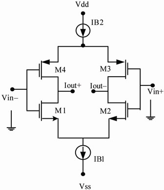
Figure 1. Traditional current output stage [11].
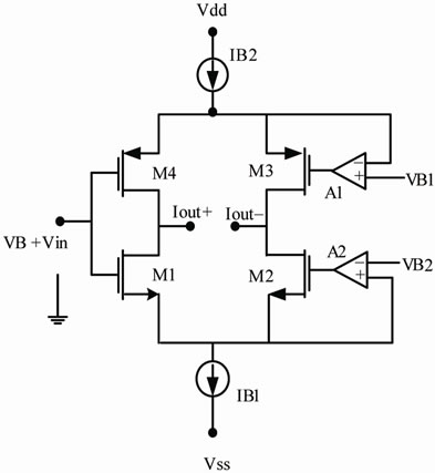
Figure 2. Simplified schematic of the COS in [11].
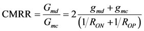
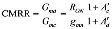
In traditional COS depicted in Figure 1, the differential and common mode transconductance, Gmd and Gmc, can be written as bellow.
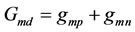 (1)
(1)
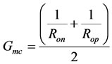 (2)
(2)
Considering (1) and (2) CMRR could be expressed as below
 (3)
(3)
n and p stand for n type and p type transistor and RO represent the output resistance of the IB1, IB2 tail current source.
In the prevalent solution which used in [11], the gate of M2 and M4 are set to constant voltage, which is usually the analog ground. This work Q1-4 shown in Figure 3 operates like quasi floating gate transistors and is used instead of normal MOS.
An idea based on eliminating common-mode signal is utilized in order to achieve high CMRR. By taking advantage of the quasi floating gate transistor, it is possible to add common-mode signal and it’s inverted one to each other. In this case CMRR is expected to improve a lot. M5 and M6 are responsible for applying CMFB which is shown in Figure 3.
Using this structure can decrease the differential mode gain inevitably; still omitting the common-mode signal which makes the common-mode gain come near to zero will increase the CMRR finally.
The schematic structure of the proposed COS is shown in Figure 3 in which M1 - M4 transistors and IB1 - IB2 tail current sources constitute the core structure of proposed COS while A1 is just an inverter with (ideally) unity common mode gain and zero differential gain one. M1 - M4 transistors would be Floating Gate type, although avoid using the expensive technology required to implement double opoly structures, they could be just regular simple MOS Transistors can be simulated/fabricated by regular common CMOS technology. However their inputs are coupled to the rest of the circuit by 10 pF capacitors as is shown in the figure.
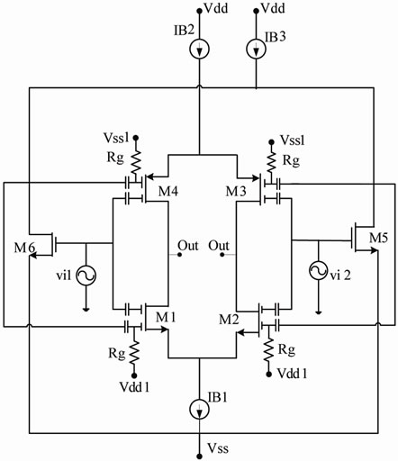
Figure 3. Schematic of the proposed COS.
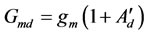
Gmd and Gmc of proposed COS is obtained as below.
 (4)
(4)
 (5)
(5)
and so
 (6)
(6)
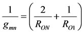
where
 (7)
(7)

 and
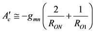
and  is the common mode and differential transconductance of CMFB circuit and RO1 represented the m1 drain-source resistance. To achieve high CMRR the CMFB circuit should have Ac = –1 and Ad ≠ –1, and it is possible if Equation (8) is established.
 (8)
(8)
3. Simulation
The proposed circuit in Figure 3 simulated with Hspice using model parameters of 0.35 µ CMOS process while the supply voltage is only ±0.75 v for acceptable comparison. In the following simulation we then compare the simulation result of the proposed COS with traditional one some other which was in other literature to allow fair comparison and emphasize the achievement.
Figure 4 exhibits the common mode transconductance gain of traditional and proposed work. (While the output load is set to 1 kΩ) and the differential gain comparison is derived in Figure 5.
CMRR diagrams are demonstrated in Figure 6 which shows 55 dB improvements in dc value of CMRR. The simulation results confirm what is mentioned before about the improvement in CMRR despite decrement of differential mode gain.
The performance characteristics of simulated COS current output stage are tabulated in Table 1 and compared with some other structures of COS. The advantage of proposed COS is apparent, especially in power dissipation, voltage supply and CMRR.
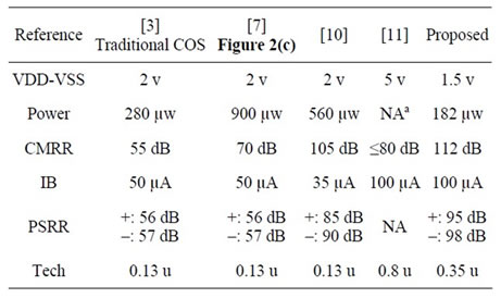
Table 1. Complete comparison between several works.
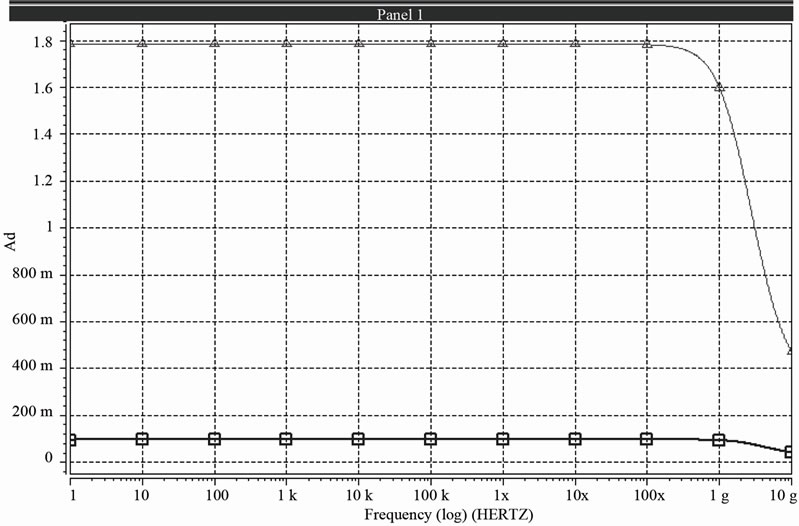
Figure 4. Magnitude of common mode transconductance gain for proposed COS(□) and traditional COS(Δ).
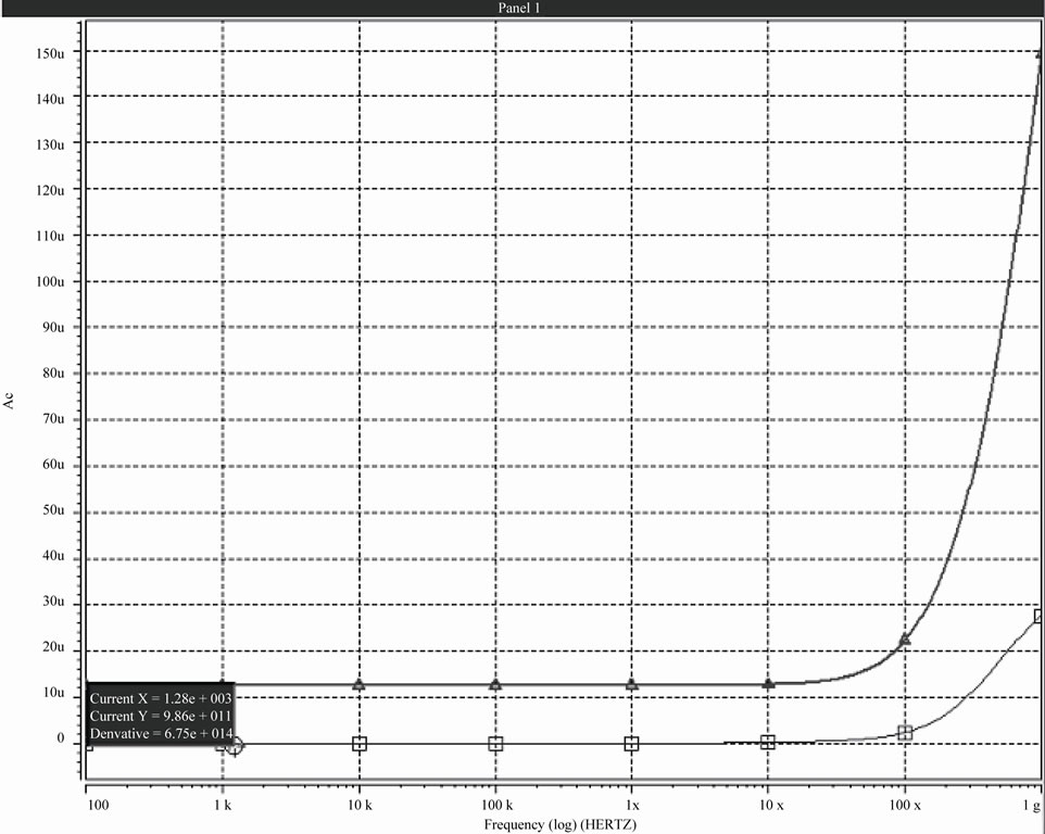
Figure 5. Magnitude of differential transconductance gain for proposed COS(□) and traditional COS(Δ).
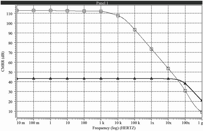
Figure 6. Magnitude of CMRR for proposed COS(□) and traditional COS(Δ).

Figure 7. Monte Carlo simulation result for proposed COS(□) and traditional COS(Δ).
To investigate the effect of technology process on performance of the proposed COS, Monte Carlo simulation are performed applying 5% mismatch on 2 important parameters of W/L, Vth. The results shown in Figure 7 indicate good robustness of the proposed COS against those mismatches.
4. Conclusion
A novel simple CMFB is used to remove common mode signal in order to achieve high CMRR in differential COS presented in this paper. It was done by taking advantage of Quasi floating gate (QFG) transistors which add the main signal and it’s opposite polarity one. Simulation results show very good improvement in CMRR, compared to others in literature. Also supply voltage and power consumption is decreased in this work.
REFERENCES
- E. Allen and M. Terry, “The Use of Current Amplifier in High Performance Voltage Application,” IEEE Journal of Solid State Circuits and Systems, Vol. 15, No. 2, 1980, pp. 155-162. doi:10.1109/JSSC.1980.1051357
- C. Toumazou, F. J. Lidgey and D. G. Haigh, Eds., “Analogue IC Design: The Current-Mode Approach,” Peter Peregrinus Ltd., London, 1993.
- S. Rajput and S. S. Jamuar, “Low Voltage Analog Circuit Design Techniques,” Circuits and Systems Magazine, Vol. 2, No. 1, 2002, pp. 24-42. doi:10.1109/MCAS.2002.999703
- G. Plamisano, C. Palumbo and S. Pennisi, “CMOS Current Amplifiers,” Kluwcr Academic Publishers, Boston, 1999. doi:10.1007/978-1-4615-5135-5
- C. Toumazou, F. Lidgey and D. Haigh, Eds., “Analogue IC Design: The Current-Mode Approach,” Peregrinus, London, 1990.
- A. F. Arbel, “Output Stage for Current-Mode Feedback Amplifiers, Theory and Applications,” Analog Integrated Circuits and Signal Processing, Vol. 2, No. 3, 1992, pp. 243-255. doi:10.1007/BF00276637
- S. Pennisi, M. Piccioni, G. Scotti and A. Trifiletti, “HighCMRR Current Amplifier Architecture and Its CMOS Implementation,” IEEE Transactions on Circuits and Systems II: Express Briefs, Vol. 53, No. 10, 2006, pp. 1118- 1122.
- J. A. De Lima and C. Dualibe, “A Linearly Tunable LowVoltage CMOS Transconductor with Improved CommonMode Stability and Its Applications to gm-C Filters,” IEEE Transactions on Circuits and Systems II: Express Briefs, Vol. 48, No. 7, 2001, pp. 649-660. doi:10.1109/82.958335
- F. Centurelli, A. D. Grasso, S. Pennisi, G. Scotti and A. Trifiletti, “CMOS High-CMRR Current Output Stages,” IEEE Transactions on Circuits and Systems II: Express Briefs, Vol. 54, No. 9, 2007, pp. 745-749. doi:10.1109/TCSII.2007.900351
- F. Centurelli, S. Pennisi and A. Trifiletti, “Current Output Stage with Improved CMRR,” 2003 IEEE International Conference on Circuits and Systems, Vol. 2, 14-17 December 2003, pp. 543-546.
- N. Larciprete, F. Loriga, P. Marietti and A. Trifiletti, “A High CMRR GaAs Single-Input to Differential Convertor,” Gallium Arsenide Application Symposium GAAS 1996, Paris, 5-7 June 1996, pp. 4-9.
- M. H. Kashtiban and S. J. Azhari, “A Novel High CMRR Low Voltage Current Output Stage,” Proceedings of 2009 IEEE International Symposium on Circuits and Systems, 9-10 July 2009, pp. 1-4.
- F. Centurelli, S. Pennisi and A. Trifiletti, “High-CMRR CMOS Current Output Stage,” Electronics Letters, Vol. 39, No. 13, 2003, pp. 945-946. doi:10.1049/el:20030602
- K.-H. Cheng and H.-C. Wang, “Design of Current Mode Operational Amplifier with Differential-Input and Differential-Output,” Proceedings of 1997 IEEE International Symposium on Circuits and Systems, Vol. 1, 9-12 June 1997, pp. 153-156.
- I. Mucha, “Current Operational Amplifiers: Basic Architecture, Properties, Exploitation and Future,” Analog Integrated Circuits and Signal Processing, Vol. 7, No. 3, 1995, pp. 243-255. doi:10.1007/BF01250804
- E. Bruun, “Bandwidth Optimization of Low Power, High Speed CMOS Current Op Amp,” International Journal of Analog Integrated Circuits and Signal Processing, Vol. 7, 1995, pp. 11-19. doi:10.1007/BF01256443