Journal of Modern Physics
Vol.4 No.3A(2013), Article ID:29372,6 pages DOI:10.4236/jmp.2013.43A063
Theoretical Study on the Optical and Electrical Properties of AlxGa1−xN Crystals
School of Information Science and Technology, Northwest University, Xi’an, China
Email: *wangxuew@nwu.edu.cn
Received January 10, 2013; revised February 9, 2013; accepted February 17, 2013
Keywords: DFT; AlxGa1−xN Crystal; Electronic Structure; Properties
ABSTRACT
By making use of the density functional theory (DFT) of the first principles and generalized gradient approximation method, the electronic structures and properties of ideal GaN and AlxGa1−xN crystals (x = 0.25, 0.5, 0.75) have been calculated and analyzed, and the influence of the doping quantity of x on the characteristics of AlxGa1−xN has been studied. The calculation results show that optical band gap of AlxGa1−xN crystal is widened that the Eg of AlxGa1−xN can be adjusted by the x, and the absorption spectrum shifts to high-energy direction with the increase of the x, and then the Fermi energy moves to the top of valence band slightly which leads to that conductivity weakened after mixed with the Al. At the same time, the variation trends of complex dielectric function, absorption spectrum and transitivity have been made clear, and the results show that AlxGa1−xN compounds can achieve the theoretical design of photoelectric performance. In a word, AlxGa1−xN crystals are potential semiconductors with very remarkable photoelectric properties, which can be applied in the development of the diversified GaN devices.
1. Introduction
With the development of microelectronic technology, the GaN-based semiconductors, which have wide band gap, high breakdown voltage, high thermal conductivity and good physical and chemical stability [1], are regarded as the core materials of the photoelectric devices, and can apply especially in the high-temperature devices, shortwavelength devices, high-frequency and high-power devices [2,3], so their experimental methods for preparing materials and devices have been studied by many domestic and foreign scholars, and found that AlxGa1−xN crystals are formed when the different amounts of Al are doped respectively in the intrinsic GaN, and the performance of GaN crystal can be better expanded that can be used as a good blue and ultraviolet optical devices [4,5]. In theory, the electronic and optical properties of the wurtzite structure GaN has been studied in first-principle [6], and the electronic structure and optical properties of GaN (0001) surface is discussed [7], and then the effects of high doping on the band-gap for AlxGa1−xN is demonstrated by the electronic properties [8], but the optical properties of AlxGa1−xN still have not been researched systematically. According to the basic optics mechanism of semiconductors in this paper, the change status of the band-gap width is studied by changing x gradually in AlxGa1−xN, and the imaginary part of the complex dielectric function and absorption spectrum curve are analyzed and investigated in order to provide a certain theoretical basis for the experiments and future optical applications.
2. Theoretical Model and Calculation Method
2.1. Built Models
The crystal structure of the GaN model adopted in this paper is hexagonal wurtzite structure, which belongs to P63mc space group and  symmetry, and the lattice constant is a = b = 0.3189 nm, c = 0.5185 nm, α = β = 90˚, γ = 120˚ [6]. In the beginning of calculation, the GaN unicellular model is built and optimized to form stable structure, which is used to create the 2 × 2 × 2 intrinsic GaN super-cell model that is shown in Figure 1, and the intrinsic super-cell model contains 16 Ga atoms and 16 N atoms. The 2 × 2 × 2 AlxGa1−xN super-cell models are formed by doping different Al concentration of x into 2 × 2 × 2 intrinsic GaN super-cell model, which are demonstrated in Figure 2, and the distribution rules of Al atoms in 2 × 2 × 2 GaN model include: Al atoms belong to a substitutional doping, and the positions of Al atoms are as evenly distributed as possible in the model and as similar as possible to the alloy mode, and then the contents GaN unitcell 2×2×2 GaN super-cell
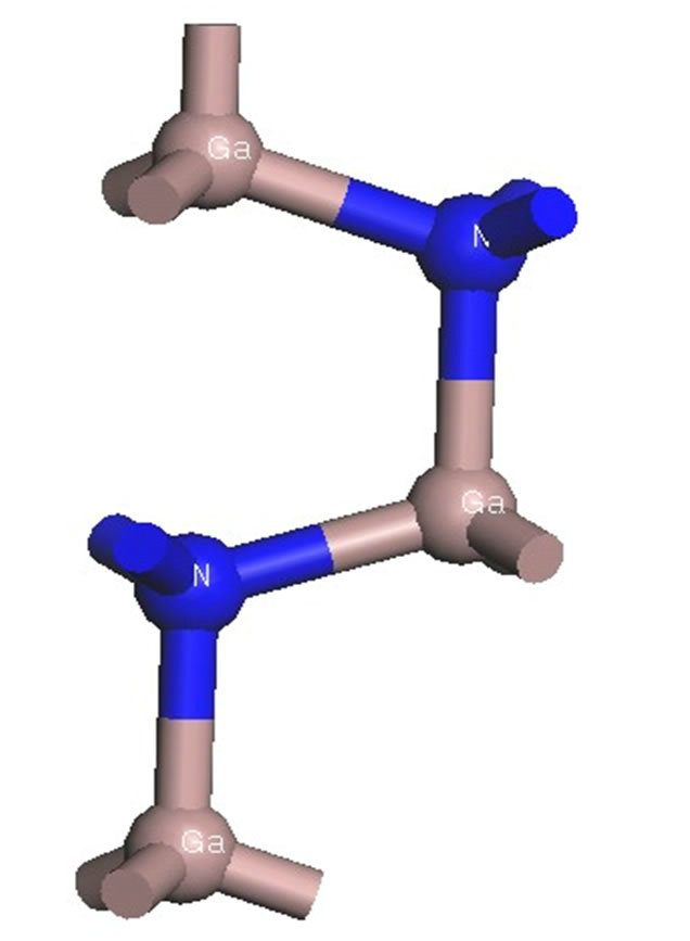

Figure 1. Structure diagrams of the intrinsic models.
 (a)
(a)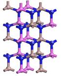 (b)
(b)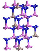 (c)
(c)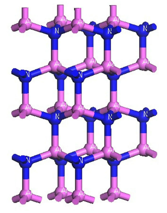 (d)
(d)
Figure 2. 2 × 2 × 2 Super-cell models of AlxGa1−xN. (a) Al0.25Ga0.75N; (b) Al0.5Ga0.5N; (c) Al0.75Ga0.25N; (d) AlN.
of Al are 25%, 50%, 75%, 100%, respectively.
2.2. Calculation Method
The calculation use the CASTEP module of MS5.0 software based on the DFT’s ab initio quantum mechanics, which adopts plane wave pseudopotential method and the exchange-correlation energy employs the PW-91 approximation method under the generalized gradient approximation (GGA). In order to ensure the convergence of system energy in the level of quasi perfect plane fundamental wave under the permission situation of the hardware resources, K grid is selected as 4 × 4 × 2 and the cutoff energy of the plane wave is 310 eV, and a single-atom convergence precision is 2.0 × 10⁻⁵ eV/atom, and then the internal stress is not more than 0.1 GPa [9].
3. The Analysis of Calculation Results
3.1. Characteristic Analysis of GaN Crystal
3.1.1. Analysis of Electrical Characteristics
The band structure of 2 × 2 × 2 GaN super-cell model can be calculated, which is shown in Figure 3. As can be seen, both the bottom of the conduction band and the top of the valence band are located on the G point of the Brillouin zone, which indicates that GaN crystal belongs to direct band-gap that is consistent with the experiment value, and its band-gap width is 1.654 eV that is different from the experimental value 3.40 eV. Because the KohnSham equation based on GGA functional ignores the impact of the surrounding electrons while used to compute the band gap, the band width is undervalued, but the result does not affect the analysis of the band-gap variation with different doping concentration in the same structure and calculation conditions. Moreover, the scissors operator should be added in order to make up the errors of the calculated band-gap widths.
The calculated electron density of states of GaN is given in Figure 4, which can be seen that the valence band of GaN is divided into three parts, including the lower valence band of −17 eV ~ −11 eV, the upper valence band of −7 eV ~ 0 eV, and the conduction band of 1.6 eV ~ 7 eV. The partial state density curves of the atoms are shown in Figure 5, wherein s, p, d, and f denote electronic sub-shell respectively. It can be seen that the lower valence band of GaN is aroused by the 3d state of Ga atoms and 2s state of N atoms, while the conduction band part is mainly composed of the 4s state and 4p state of Ga atoms and the amount provided by N is relatively less and can be ignored. The peak of electronic density of states appearing in −13 eV is provided by the 3d state of Ga atoms while the peak of electronic density of states in −15 eV is supplied by the 2s state of N atoms.
3.1.2. The Analysis of Optical Characteristic
Considering the relationship between the absorption
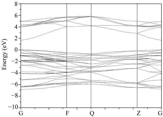
Figure 3. The band structure of GaN.
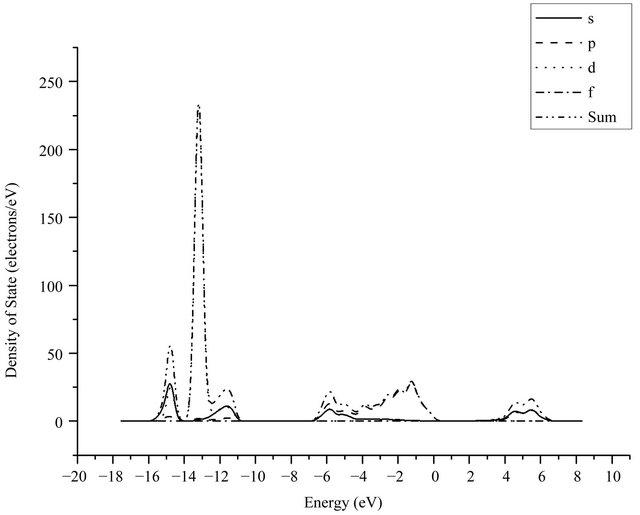
Figure 4. The electronic density of states of GaN.
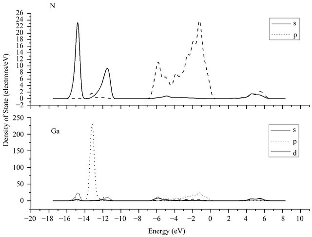
Figure 5. Partial density of states of Ga atoms and N atoms.
coefficient and the complex refractive index [6], the interaction between phonon and electron of the crystal can be expressed by the time-dependent perturbation including in the wave function of the electronic ground state, and the mutual interference of the phonon and the electric field can cause the transition between the electronic occupied state and unoccupied state, which can be related to the connection between the density of states of the conduction band and the valence band and result in the spectra generated by the excited states. Because the absorption coefficient α of the semiconductor is related to the imaginary part  of its dielectric constant and the reflectivity coefficient R is related to the real part
  of its dielectric constant and
  and
and 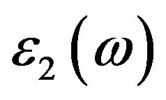 of GaN must be first calculated out, which can be given by the following formula [10,11]:
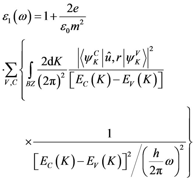 (1)
(1)
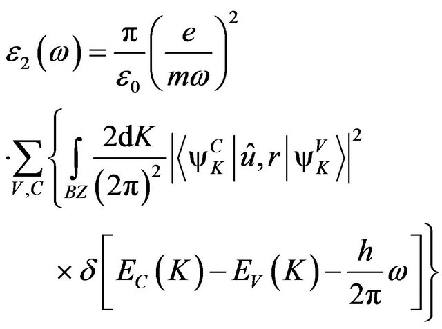 (2)
(2)
In the formula, K is the wave vector of electron, C and V are the valence band and conduction band, BZ is the first Brillouin zone, Ψ is the wave function, û is electric vector,  and
and  are the intrinsic energy levels on conduction band and valence band.
By calculating 2 × 2 × 2 intrinsic GaN super-cell model in Figure 1, the complex dielectric function and the absorption spectrum of GaN crystal are shown in Figures 6 and 7. From the imaginary part-dashed line in Figure 6, it can be seen that 5 peaks appear at the range of 3 eV ~ 23 eV that are located at 4.5 eV, 6.8 eV, 7.7 eV, 9.5 eV, 13 eV, separately. The main peak at 7.7 eV that broadens in 5 eV ~ 12 eV is caused by the transitions between the remote bands. The peak at 4.5 eV corresponds to the direct transitions from the bottom of valence band to the top of conduction band, which is brought mainly about by the transitions of 3p state orbit electrons of Ga atoms. Three dielectric peaks in 7.7 eV, 9.5 eV, 13 eV may be caused by the transitions from lower valence band to the upper valence band, which may be from 3d state of Ga atoms and 2s state of N atoms in lower valence band or the 3p state of Ga atoms and 2p state of N atoms in upper valence band. Secondly, the peak in 20 eV is very weak, which is mainly caused by transitions from the lower valence band to the conduction band, since the atoms involving the transition mode are very few. Comparing Figure 6 with Figure 7, the peak positions in the absorption spectra are very close
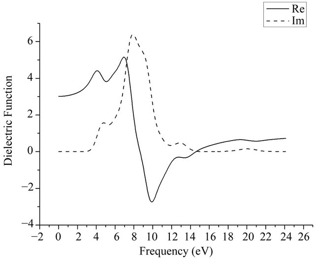
Figure 6. Complex dielectric function of GaN.
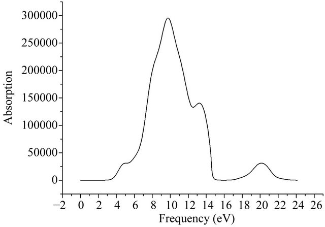
Figure 7. Absorption spectra of GaN.
to ones of the complex dielectric function, but the difference of the peak strength are relative large. The strongest peak of the absorption spectrum situates at 9.5 eV approximately, which is from the transitions of 3d state electron of Ga and 2p state electron of N in Figure 5.
By using the equations above, the transmittance 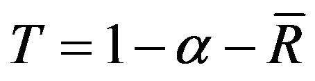 (α is the absorption coefficient,
  is the normalized reflection coefficient R) can be deduced and calculated, as shown in Figure 8, from which it can be seen that the change of transmittance is irregular before 350 nm and reaches gradually smooth state in the range of visible light after 350 nm, and the transmisivity can achieve 92% ~ 94%.
3.2.1. Analysis of Electrical Characteristics
A series of band structures of AlxGa1−xN crystal models mixed with different Al component of 25%, 50%, 75%, and 100% are calculated respectively, and the band-gap widths are listed in Table 1. Because the conduction bands are underestimated by the error of the calculation

Figure 8. Optical transmittance of intrinsic GaN crystal.
Table 1. The band-gap under the different concentrations of Al compositions.
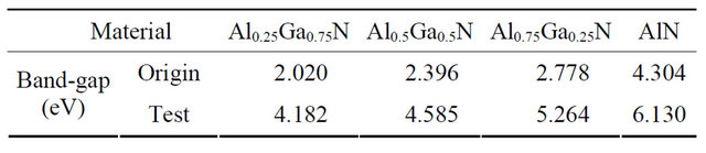
software, the band gap values of the theoretical calculation, namely “Origin values” are very low, and the Test values are the ones modified by adding the scissor difference.
The curve of density of states of Al0.5Ga0.5N crystal is computed as Figure 9, and the band-gap width is about 2.396 eV which is counted from the conduction band of 3 eV ~ 7 eV to the upper valence band of −6 eV ~ 0 eV while the part of the lower valence band is −15 eV ~ −11 eV. The conduction band is caused by the 4s state and 4p state electrons of Ga atoms and 2p state electron of N atoms, and the upper valence band is aroused by the 4s state electrons of Ga atoms and 2p state electrons of N atoms while the lower valence band is mainly dominated by 3d state electron of Ga atoms. It can be seen that the energy band is mainly distributed in the range of −15 eV ~ 7 eV, and the peak at −13 eV is very strong which has nothing to do with the surrounding valence bands. By comparison in detail, the energy band structure of AlxGa1−xN above is similar to one of the intrinsic GaN, and the band positions are almost unanimous and the band widths just become bigger, which is formed by the movement of conduction band to the high energy region and the a little shift of Fermi level to the top of valence band, so that the conductivity weakens. But in the structure, two new peaks of electronic density of states appear in the positions of −14 eV and −11.8 eV which should be brought about by Al doping.
3.2.2. Optical Characteristics Analysis
The imaginary part of dielectric function of Al0.5Ga0.5N is calculated and shown in Figure 10. It is found that 4

Figure 9. Density of states of Al0.5Ga0.5N.
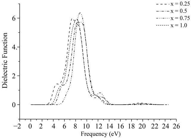
Figure 10. The imaginary of complex dielectric function of AlxGa1−xN.
peaks are degenerated by 5 peaks of GaN while the peak positions of Al0.5Ga0.5N move slightly to high energy region, and the main peak is located at 8 eV whose peak value did not change basically, which is resulted from that the optical band gap become wide after the Al doped and shows the electronic transitions of Al0.5Ga0.5N is more different than GaN. As can be seen from the above curves, the dielectric peak values slightly increase and the peak position keeps moving to the high energy region with the amount increasing of Al doping.
Figure 11 gives out the absorption spectrum of AlxGa1−xN. As can be seen, the more the number of Al atoms which are doped in GaN is, the higher the energy appearing the light absorption peak is. While the positions of the main peaks slightly move to the right along with the increase of Al doping, the positions of the peaks at 4.5 eV, 13 eV and 20.1 eV are not almost changed, and the intensities of peaks at 4.5 eV and 20.1 eV weaken and even disappear, but the peak value at 13 eV fluctuates. It indicates that the performance before and
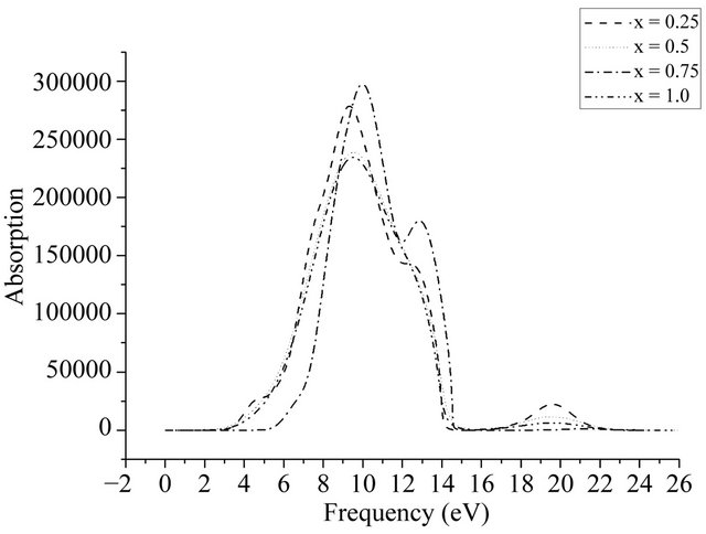
Figure 11. The absorption spectrum of AlxGa1−xN.
after Al doping doesn’t have large change and the position shift of the strongest peak is due to that optical band gap of AlxGa1−xN becomes large.
The optical transmittance curve of Al0.5Ga0.5N is similar substantially to Figure 8, and the optical transmittance reaches the steady state at about 260 nm that wavelength is shorter, and its transmission rate is about 93%, which indicates that the optical performance of AlxGa1−xN is better than GaN.
4. Conclusion
The photoelectric characteristics of the intrinsic supercell GaN crystal and the substitutional supersell AlxGa1−xN models with the different components of x have been calculated and analyzed, and the results demonstrates that the conduction band with the increase of the Al concentration moves to high energy region, and the bandgap width becomes bigger and Fermi level slightly moves to the top of valence band, which can lead to that the valence electrons in AlxGa1−xN with the x increase are bounded tighter while the energy of the valence electrons drops to the lower than ones of GaN, so the weaker the conductivity of AlxGa1−xN is, the bigger x is. Secondary, the absorption spectrum moves to the high energy direction, and the range of transmittance becomes wide. In short, the photoelectric performance by incorporation of a certain proportion of Al can be adjusted, which is consistent with the trend of experimental data and provides a theoretical basis for the application of GaN-based materials.
5. Acknowledgements
One of us (all authors) thanks the support of the National Science Foundation (61076002) and Shaanxi Education Commission (2010 JK848).
REFERENCES
- I. Yonenaga, “Thermo-Mechanical Stability of Wide-BandGap Semiconductors: High Temperature Hardness of SiC, AlN, GaN, ZnO and ZnSe,” Physica B: Condensed Matter, Vol. 308-310, 2001, pp. 1150-1152. doi:10.1016/S0921-4526(01)00922-X
- A. Goswami, R. J. Trew and G. L. Bilbro, “Physics Based Modeling of Gate Leakage Current Due to Traps in AlGaN/GaN HFETs,” Solid-State Electronics, Vol. 80, 2013, pp. 23-27. doi:10.1016/j.sse.2012.10.005
- F. X. Wang, H. Lu, X. Q. Xiu, D. J. Chen, P. Han, R. Zhang and Y. D. Zheng, “Leakage Current and Sub-Bandgap Photo-Response of Oxygen-Plasma Treated GaN Schottky Barrier Diodes,” Applied Surface Science, Vol. 257, 2011, pp. 3948-3951.
- S. J. Chang, T. K. Ko, J. K. Sheu, S. C. Shei, W. C. Lai, Y. Z. Chiou, Y. C. Lin, C. S. Chang, W. S. Chen and C. F. Shen, “AlGaN Ultraviolet Metal-Semiconductor-Metal Photodetectors Grown on Si Substrates,” Sensors and Actuators A: Physical, Vol. 135, No. 2, 2007, pp. 502-506. doi:10.1016/j.sna.2006.09.017
- D. Fu, R. Zhang, B. G. Wang, B. Liu, Z. L. Xie, X. Q. Xiu, H. Lu, Y. D. Zheng and G. Edwards. Ultraviolet Emission Efficiencies of AlxGa1−xN Films Pseudomorphically Grown on AlyGa1−yN Template (x < y) with Various Al-Content Combinations,” Thin Solid Films, Vol. 519, No. 22, 2011, pp. 8013-8017.
- S. Li, C. Y. Ouyang, “First Principles Study of Wurtzite and Zinc Blende GaN: A Comparison of the Electronic and Optical Properties,” Physics Letters A, Vol. 336, No. 2-3, 2005, pp. 145-151.
- Y.-J. Du, B.-K. Chang, J.-J. Zhang, B. Li and X.-H. Wang, “First-Principles Study of the Electronic Structure and Optical Properties of GaN (0001) Surface,” Acta Physico-Chimica Sinica, Vol. 61, No. 6, 2012, Article ID: 067101.
- N. Safta, H. Mejri, H. Belmabrouk and M. A. Zaïdi, “Effects of High Doping on the Bandgap Bowing for AlxGa1−xN,” Microelectronics Journal, Vol. 37, No. 11, 2006, pp. 1289- 1292. doi:10.1016/j.mejo.2006.07.010
- O. Arbouche, B. Belgoumène, B. Soudini and M. Driz, “First Principles Study of the Relative Stability and the Electronic Properties of GaN,” Computational Materials Science, Vol. 47, No. 2, 2009, pp. 432-438.
- Y. J. Du, B. K. Chang, X. Q. Fu, X. H. Wang and M. S. Wang, “Electronic Structure and Optical Properties of ZincBlende GaN, Optik,” International Journal for Light and Electron Optics, Vol. 123, No. 24, 2012, pp. 2208-2212. doi:10.1016/j.ijleo.2011.10.017
- X. C. Li, “Principles Calculations of the Electronic Structures and Optical Properties of Oxygen Passivated 4HSiC Nanostructures [D],” Nankai University, Tianjin, 2010.
NOTES
*Corresponding author.