Journal of Modern Physics
Vol.3 No.9(2012), Article ID:22677,8 pages DOI:10.4236/jmp.2012.39124
Effect of Concentration on the Optical and Solid State Properties of ZnO Thin Films Deposited by Aqueous Chemical Growth (ACG) Method
1Department of Science Laboratory Technology, School of Applied Sciences, Rivers State Polytechnic, Bori, Nigeria
2Department of Physics, Faculty of Science, Rivers State University of Science and Technology, Port Harcourt, Nigeria
3Department of Physics and Astronomy, University of Nigeria, Nsukka, Nigeria
Email: sylvestermammah@yahoo.com, erfopara2002@yahoo.com, fiezema@yahoo.com, sabroze@yahoo.com
Received July 11, 2012; revised August 15, 2012; accepted August 24, 2012
Keywords: Component; Formatting; Style; Styling; Insert
ABSTRACT
Thin films of Zinc Oxide (ZnO) having different concentrations were deposited using the Aqueous Chemical Growth (ACG) method. The films were characterized using Rutherford Back Scattering (RBS) spectroscopy for chemical composition and thickness, X-Ray Diffraction (XRD) for crystallographic structure, a UV-VIS spectrophotometer for the analysis of the optical and solid state properties which include spectral absorbance, transmittance, reflectance, refractive index, direct band gap, real and imaginary dielectric constants, absorption and extinction coefficients and a photomicroscope for photomicrographs. The average deposited film thickness was 100 nm. The results indicate that the values of all the optical and solid state properties investigated vary directly with concentration except transmittance which is the reverse. Thus, the optical and solid state properties of ZnO thin film deposited by the Acqueous Chemical Growth method can be tuned by deliberately controlling the concentration of the precursors for various optoelectronic applications including its application as absorber layer in solar cells.
1. Introduction
Zinc Oxide is an amphoteric oxide which exists in the form of white powder (zinc white) at room temperature [1]. Though zinc oxide exists naturally in the earth crust (zincite), it is the synthetic ZnO produced in laboratories that are usually used in industries [2].
Crystalline zinc oxide is thermochromic [3]. Apart from the ability of ZnO to react with acids, it also reacts with bases to produce soluble zincates [4-6]. Zinc oxide has high stability at room temperature and decomposes into zinc vapour and oxygen at about 1975˚C [7]. Though zinc oxide can exist in either of hexagonal wurtzite, cubic zinc blende and cubic (rock salt) structure, the hexagonal wurtzite structure is the most common at room temperature. The different polymorphs of ZnO do not possess the property of symmetry inversion. This and other properties such as ionic bonding account for the strong piezoelectricity of both hexagonal and zinc blende ZnO [8,9].
The hexagonal wurtzite structure has the point group 6 mm (Hermann-Mauguin notation) or C6v (schoenflies notation) and a space group of P63me or . Its lattice constants are a = 3.25 Å and C = 5.2 Å [10].
The many applications to which ZnO can be put has made it to be a material for constant scientific study. The diverse applications of ZnO are derived from its unique properties which include non-toxicity, good electrical conductivity, high luminous transmittance, good substrate adherence, good optical behaviour and stability in plasma atmosphere [11,12].
ZnO has been tested and found to behave as a semiconductor having a wide bulk direct band gap of about 3.37 ev at room temperature [13] ZnO has been used for the fabrication of light emitting diodes, varistors, photo detectors, piezoelectric cantilever, gas sensors, buffer layer in solar cells and in photonic crystals [14-21].
As a result of the strategic importance of ZnO to humanity, various deposition methods have been used for its production in the form of thin films. Among these methods are the chemical bath deposition (CBD) [22-26].
Successive Ionic Layer Adsorption and Reaction (SILAR) method [27,28].
Spray pyrolysis method [29].
Electro deposition method [30,31].
The ACG method is a novel method for the deposition of ZnO thin films; hence the literature on it is sparse.
Indeed F. I. Ezema (2004) [26] reported that “Thin films of ZnO have been used but its preparation techniques have been restricted to sputtering, vacuum evaporation, chemical vapour deposition, spray prolysis, molecular beam epitaxy, sol gel and pulse laser”.
Among the advantages which the ACG method have over the other methods are simplicity, low cost, reproducibility, availability of materials, environmental friendliness (non toxicity of residue), non requirement of surfactant, templates and complexing agents, low temperature requirements, ability to produce nanostructures, high purity (absence of surfactants), suitability for large scale production etc. [32,33].
This paper reports the effect of concentration of precursors on the optical and solid state properties of ZnO thin films deposited using the ACG method with Zn(NO3)2 6H2O as precursor material. The spectral analysis of the optical and solid state properties was carried out using a Unico UV-2102 PC spectrophotometer.
2. Experimental Details
ZnO thin films were deposited on clean glass slides using Aqueous Chemical Growth method.
Equimolar concentrations of hydrated zinc nitrate (Zn(NO3)2·6H2O) and hexamine in 80 ml of water were used as precursors.
Hexamine was used to make the zinc nitrate alkaline. Three samples having different concentrations of the precursors were prepared as shown in Table 1 below.
Masses of samples were measured using an analytical microbalance. The masses of the components of each sample were put into a 100 ml pyrex bottle together with 80 ml of water. The contents were properly mixed using a magnetic stirrer.
The pyrex bottles were then tightly corked and care fully placed in an oven at a temperature of 90.00˚C.
The average deposition time for the films was twelve hours.
The chemical reactions which resulted in the crystallization of ZnO are:
C6H12N4 + 6H2O ® 6HCHO + 4NH3
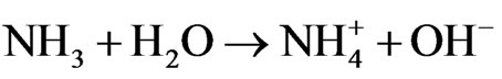
2OH− + Zn2+ ® ZnO + H2O [34]
3. Results and Discussion
The elemental composition of sample C2 was analyzed using Rutherford Backscattering (RBS).
The result is as shown in Figure 1. Judging from the film composition shown in the Table 2 below, we conclude that the elements contained in sample C2 are Zn (0.050) and oxygen (0.950) while the glass substrate has the composition O (0.500), Si (0.120), Ca (0.100), Al (0.100) and Na (0.180). This is summarized in Table 2. The thickness of the film is given as 100 nm.
The X-Ray diffractogram of the ACG ZnO thin films were studied to determine its crystalline nature.
![]() The thin films were scanned continuously between 0 and 70 at step size of 0.03 and at time per step of 0.15 s. The Figure 2 below shows the intensity of peaks versus diffraction angle 2θ for sample C2 ZnO thin film using CuKα radiation source having a wavelength of 1.54056 Å. The X-ray diffractogram reveal several peaks corresponding to directions of strong reflections. Some of the observed peaks are 30.00˚, 32.50˚, 34.42˚, 45.56˚ and 54.87˚, and 67.50˚.
The thin films were scanned continuously between 0 and 70 at step size of 0.03 and at time per step of 0.15 s. The Figure 2 below shows the intensity of peaks versus diffraction angle 2θ for sample C2 ZnO thin film using CuKα radiation source having a wavelength of 1.54056 Å. The X-ray diffractogram reveal several peaks corresponding to directions of strong reflections. Some of the observed peaks are 30.00˚, 32.50˚, 34.42˚, 45.56˚ and 54.87˚, and 67.50˚.
The 34.42˚ agree with the preferred orientation along the (002) plane reported by Ajuba et al. (2010) [35] and Shinde et al. (2005) [36] who used the CBD and SILAR methods respectively. Also, the 67.50˚ fairly agree with the (112) plane reported by Ajuba et al. (2010) [35,36].
The diffractogram reveal sharp diffraction peaks which is indicative of good crystallinity [37-41].
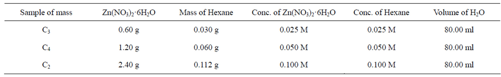
Table 1. Three samples of different concentrations of the precursor.
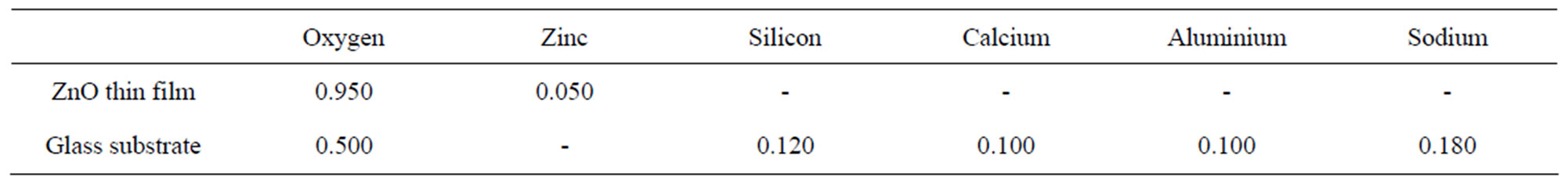
Table 2. Elemental composition of ZnO thin film and substrate from RBS analysis.
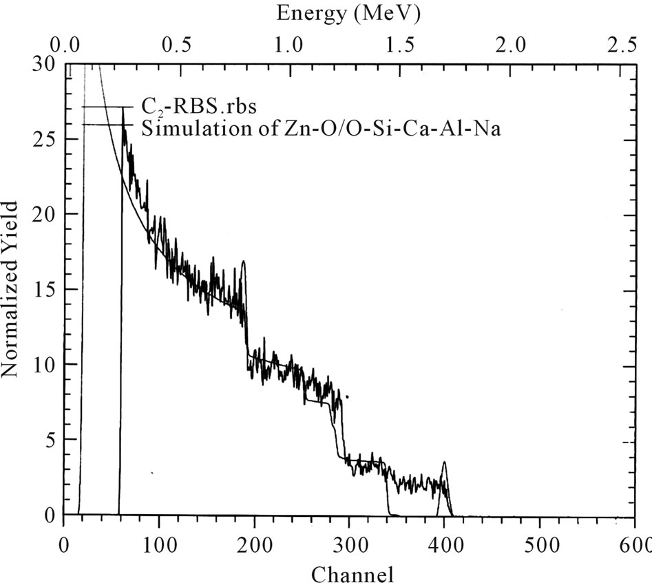
Figure 1. RBS analysis for ACG ZnO thin film (sample C2).
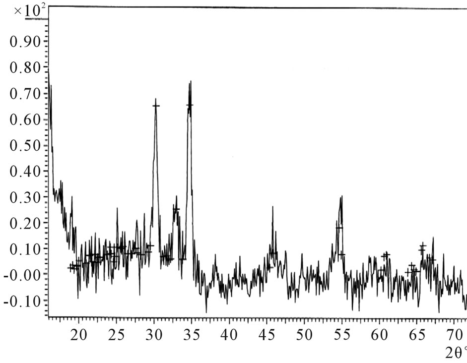
Figure 2. X-Ray diffractogram for ACG ZnO thin film (sample C2).
The XRD pattern shows that film is crystallized in the wurtzite ZnO hexagonal P6(3) mc structure. (JCPDF CARD no. 36-1451) [42].
The mean size of the crystallite was estimated to be 12 nm using the Sherrer formula which is given as:
 (1)
(1)
where K = 0.9
 =1.541 Å is the diffraction peak angle (34.42˚) and β is the Full Width at Half Maximum (FWHM) corresponding to the diffraction peak.
The spectral absorbance of films is as shown in Figure 3.
The 0.05 M concentration has an average absorbance value of 0.28 in the visible region while the 0.025 M concentration has an average absorbance value of 0.268 in the visible region.
However, the 0.05 M concentration has the lowest absorbance value of 0.21 in the infrared region.
Absorption peaks clearly occurred in film C2 at 368 nm, 496 nm and 656 nm but were not so clearly defined in films C3 and C4. Ezema [26] reported absorption peaks at 3.68 nm, 449 nm and 566 nm using Chemical Bath Method. The difference in the absorption peaks may be due to deposition method. The spectral transmittance of the films is as shown in Figure 4. Transmittance decreases with concentration in the visible region. The 0.1 M, 0.05 M and 0.025 M concentrations has average transmittance of 45.5%, 53.2% and 54.60% respectively in the visible region.
However, the 0.05 M concentration has the highest transmittance of about 61.8% in the ultraviolet region. The transmittance of the films in the visible region is generally lower than the above 85% transmittance reported using Chemical Bath Deposition method [43].
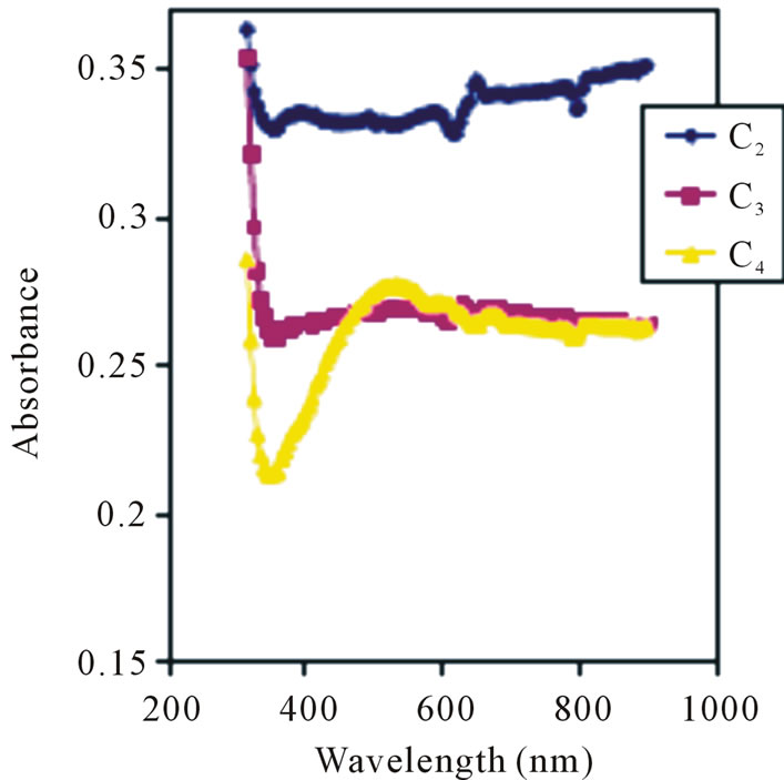
Figure 3. Absorbance vs. wavelength for ZnO thin film at different conc.
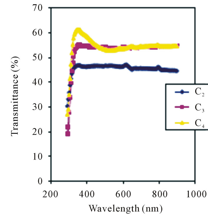
Figure 4. Transmittance vs. wavelength for ZnO thin films at different conc.
It is also much lower than the 90% 95% transmittance in the UV-VIS-NIR regions for ZnO thin films deposited using spray pyrolysis method [44,45] and Sol Gel method [46].
It has been reported that the transmittance of a film increases as its thickness decreases [26].
The average thickness of the films being reported on is 100 nm which is far smaller than the 0.203 μm and 0.069 μm thicknesses which gave average transmittances of 62% and 75% respectively that has been reported [26]. Thus, the transmittance of films deposited by ACG method are relatively lower compared to the ones deposited by other methods even though the thicknesses are smaller. The spectral reflectance of the films being reported on is as shown in Figure 5. Reflectance increases with concentration in the visible region.
The 0.1 M, 0.050 M and 0.025 M concentrations reflect an average of 20.25%, 19.38% and 18.88% of visible electromagnetic waves. These values are higher than the average of 12% to 17% reflectance of films deposited using Chemical Bath Method as reported by Ezema [26].
Thus, films deposited by ACG method are better reflectors than those deposited by Chemical Bath Method. Absorption coefficient increases with concentration in the visible region as shown in Figure 6.
The average absorption coefficients for the 0.025 M, 0.05 M and 0.1 M concentrations are 0.62, 0.65 and 0.77 respectively. However, in the UV region, 0.05 M has the lowest absorption coefficient of about 0.49.
Refractive index is fairly constant in the visible region as shown in Figure 7. The 0.1 M, 0.05 M and 0.025 M concentrations have average refractive indices of 2.3, 2.225 and 2.2 respectively. However, the 0.05 M concentration has the lowest refractive index of about 2.05 in the UV region.
It has been reported that the refractive index of ZnO films doped with Li deposited by spray pyrolysis lie between 1.60 and 2.20 at a wavelength of 500 nm [45], while Ezema [26] gave the average refractive index of the ZnO films deposited by Chemical Bath method as being between 1.64 and 1.98 and also reported observed peak values of 2.28 at 368 nm and 1.72 at 569 nm. In our own case, the refractive indices for the different concentrations were generally uniform in the visible region.
Extinction coefficient decreases with concentration and also decreases with increasing photon energy (wavelength) in the visible region as shown in Figure 8. The value of extinction coefficient for 0.1 M concentration ranges from 37.85 × 10⁻³ for 2 eV to 27.14 × 10⁻³ for 3 eV in the visible region. Similarly, the values of extinction coefficient for 0.05 M concentration ranges from 35 × 10−3 for 2 eV to 19.64 × 10⁻³ for 3 eV and that of the 0.025 M concentration ranges from 30 × 10−3 to about 21.43 × 10⁻³ at 3 eV in the visible region.
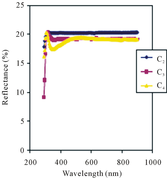
Figure 5. Reflectance vs. wavelength for ZnO thin films at different conc.
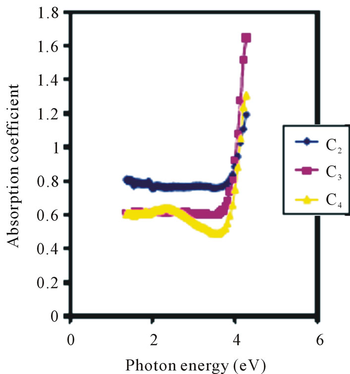
Figure 6. Absorption coefficient vs. photon energy for ZnO at different conc.
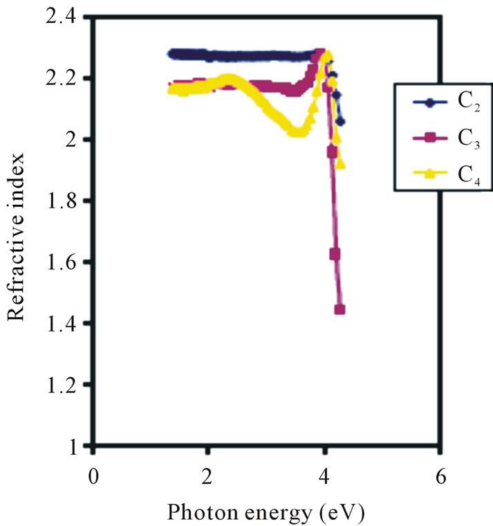
Figure 7. Refractive index vs. photon energy for ZnO thin films at different conc.
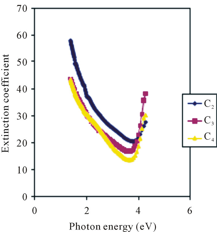
Figure 8. Extinction coefficient vs. photon energy for ZnO thin films at different conc.
However, the 0.05 M concentration has the lowest extinction coefficient of about 13.93 × 10⁻³ in the ultraviolet region. In general all the concentrations have the lowest value of extinction coefficient in the higher energy region (between 3 eV and 4 eV) and the maximum value in the low energy region (between 1 eV and 2 eV). Low and high values of extinction coefficient at high and low energy regions respectively have been reported [26].
The band gap increases with concentration as shown in Figure 9. The average band gap for the 0.025 M, 0.05 M and 0.1 M concentrations are 1.16 eV, 1.22 eV and 1.4 eV respectively.
These values are lower than the direct band gaps of ZnO films deposited by Chemical Bath method [26] which lie between 1.60 eV and 1.80 eV.
Our values are also far lower than 3.29 eV band gap obtained for aluminium doped ZnO deposited using radio frequency (r.f) megnetron sputtering [18], and intrinsic band gap of 3.20 eV for ZnO films deposited by spray pyrolysis [29]. The low values of the direct band gap obtained indicate that the ZnO thin film materials prepared by ACG method are suitable for use as absorber layers in solar cells. The low values of the band gaps obtained in this work may be due to preparation conditions Ezema et al. [26].
Real dielectric constant increases with concentration in the visible region as shown in Figure 10. The 0.025 M, 0.05 M and 0.1 M concentrations have average real dielectric constants of 4.76, 4.85 and 5.15 respectively in the visible region of the electromagnetic spectrum.
However, the 0.05 M concentration has the lowest real dielectric constant of about 4.09 in the ultra-violet region. Figure 11 is the Imaginary dielectric constant that increases with concentration in the visible range.
The 0.1 M, 0.05 M and 0.025 M concentrations have average values of imaginary dielectric constant which
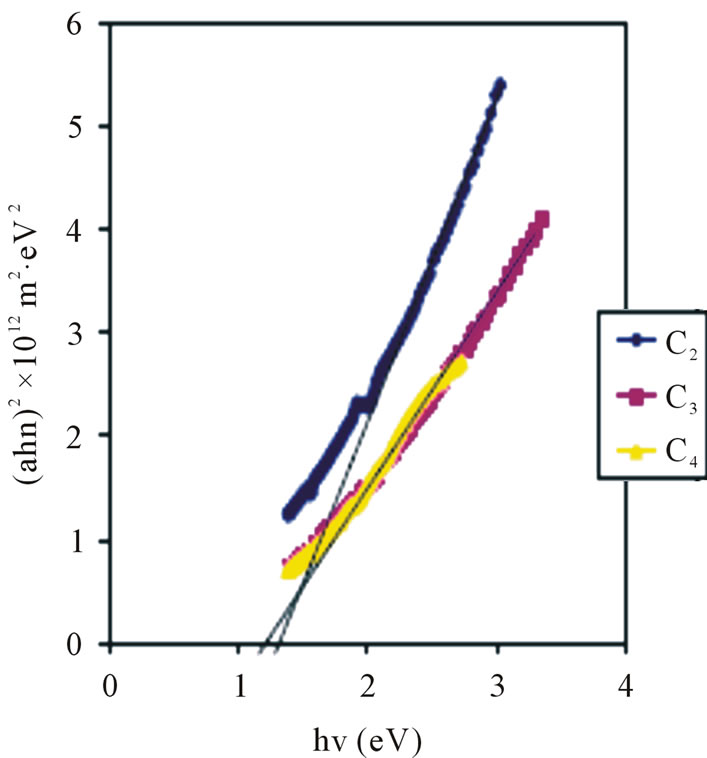
Figure 9. Direct band gap plot for ZnO thin films at different conc.
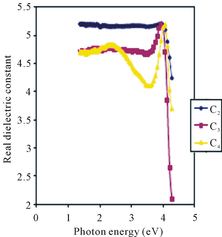
Figure 10. Real dielectric constant vs. photon energy for ZnO thin films at different conc.
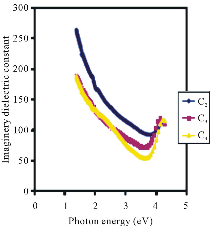
Figure 11. Imaginery dielectric constant vs. photon energy for ZnO thin films at different conc.
ranges from 180.3 × 10⁻³ for 2 eV to 118.18 × 10⁻³ for 3 eV, 143.93 × 10⁻³ for 2 eV to 78.785 × 10⁻³ for 3 eV and 143.93 × 10⁻³ for 2 eV to 89.39 × 10⁻³ for 3 eV respectively. This shows that the imaginary dielectric constant decreases with increasing photon energy (decreasing wavelength) for all concentrations in the visible region.
However, the 0.05 M concentration has the lowest imaginary dielectric constant of about 56.06 in the ultra violet region. All concentrations have their lowest imaginary dielectric constant values in the ultra-violet region.
The photomicrographs as shown in Figure 12 indicate uniform deposition of the ZnO thin films on the glass substrate. While C2 and C3 show stretches of rod C4 shows clusters of thin films on the substrates.
4. Conclusions
Crystals of ZnO have been successfully grown on glass
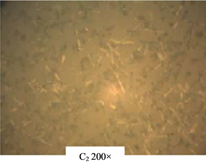
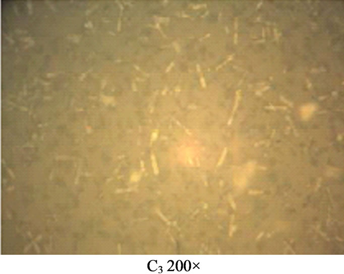
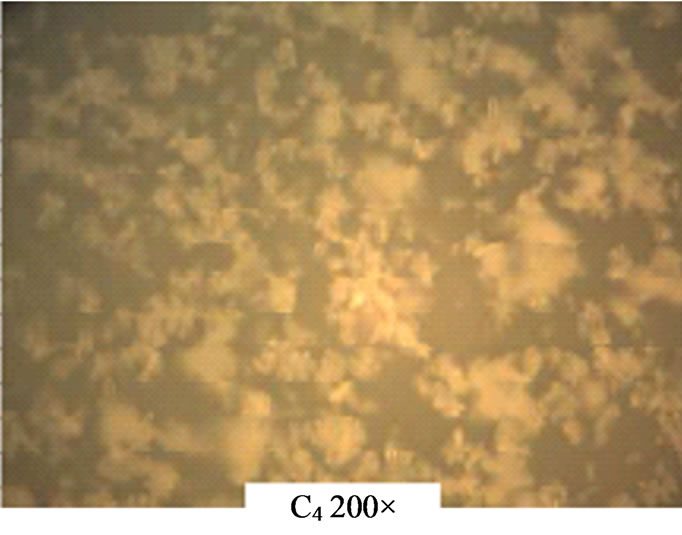
Figure 12. Photomicrographs of ACG ZnO thin films.
slides in the form of thin films from the aqueous solution of hexahydrated zinc nitrate and hexamine after the fashion of Lionel Vassieres [47]. The concentration of the precursors was found to vary directly with absorbance, reflectance, absorption coefficient, extinction coefficient, refractive index, direct band gap, real dielectric constant and imaginary dielectric constant. The transmittance of the thin films was found to vary inversely with the concentration of the precursors.
The results indicate the suitability of ZnO thin films prepared by the Aqueous Chemical Growth method for various optoelectronic applications such as absorber layer in solar cells.
REFERENCES
- T. Kiyoshi, Y. Akihiko and S. Adarsh, “Wide Bandgap Semiconductors: Fundamental Properties and Modern Photonic and Electronic Devices,” Springer, Heidelberg, 2007, p. 257.
- C. Klingshirn, “ZnO: Material, Physics and Applications,” Physical Chemistry, Vol. 8, No. 6, 2007, pp. 782-803. HUdoi:10.1002/cphc.200700002U
- E. Wiberg and A. F. Holleman, “Inorganic Chemistry,” Elsevier, Amsterdam, 2001.
- J. W. Nicholson, Journal of Materials Science, Vol. 33, No. 225, 1998.
- J. L. Ferracane, “Material in Dentistry: Principles and Application,” Lippincott Williams & Wilkins, Philadelphia, 2001.
- C. K. Park, M. R. Silsbee and D. M. Roy, “Setting Reaction and Resultant Structure of Zinc Phosphate Cement in Various Orthophosphoric Acid Cement-Forming Liquids,” Cement and Concrete Research, Vol. 28 No. 1, 1998, pp. 141-150. doi:10.1016/S0008-8846(97)00223-8UH
- N. N. Greenwood and A. Earnshaw, “Chemistry of the Elements,” Butterworth-Heinemann, Oxford, 1997.
- U. Özgür, Y. T. Alivov, C. Liu, A. Teke, M. A. Reshchikov, S. Doğan, V. Avrutin, S. J. Cho, et al., “A Comprehensive Review of ZnO Materials and Devices,” Journal of Applied Physics, Vol. 98, No. 4, 2005, Article ID: 041401.
- S. Baruah and J. Dutta, “Hydrothermal Growth of ZnO Nanostructures,” Science and Technology of Advanced Materials, Vol. 10, No. 1, 2009, Article ID: 013001.
- U. Rossler, “Landolt-Bornstein, New Series, Group III,” Springer, Heidelberg, 1999.
- T. Mahalingam, V. S. John, M. Raja, Y. K. So and P. J. Sabastian, “Electrodeposition and Characterization of Transparent ZnO Thin Films,” Solar Energy Materials and Solar Cells, Vol. 88, No. 2, 2005, pp. 227-235.
- Y. R. Shinde, T. P. Gujar, C. D. Lokhande, R. S. Nane and S. H. Han, Materials Chemistry and Physics, Vol. 326, 2006.
- A. E. Ajuba, S. C. Ezugwu, P. U. Asogwu and F. I. Ezema, Chalcogenide Letter, Vol. 10, 2010, pp. 573-579.
- T. Soki, Y. Hatanaka and D. C. Look, “ZnO Diode Fabricated by Excimer-Laser Doping,” Applied Physics Letters, Vol. 76, No. 22, 2000, pp. 3257-3259.
- Y. Lin. C. R. Gorla, S. Linng, N. Emanetoglu, Y. Tor, H. Shen and M. Wraback, ‘Ultraviolet Detectors Based on Epitaxial ZnO Films Grown by MOCVD,” Journal of Electronic Materials, Vol. 29, No. 1, 2000, pp. 69-74.
- V. R. Shinde, T. P. Gujar and C. D. Lokhande, “LPG Sensing Properties of ZnO Films Prepared by Spray Pyrolysis Method: Effect of Molarity of Precursor Solution,” Sensors and Actuators H, Vol. 120, No. 2, 2007, pp. 551-559.
- A. Ennaoui, S. Siebentrith, M. Ch. Lux-Steiner, W. Riedl and F. Karg, “High-Efficiency Cd-Free CIGSS Thin-Film Solar Cells with Solution Grown Zinc Compound Buffer Layers,” Solar Energy Materials and Solar Cells, Vol. 67, No. 1-4, 2002, pp. 31-40.
- Y. Chen, D. Bagnall and T. Yao, “ZnO as a Novel Photonic Material for the UV Region,” Materials Science and Engineering B, Vol. 75, No. 2-3, 2000, pp. 190-198.
- S. Liang, H. Sheng, Y. Liu, Z. Hio, Y. Lu and H. Shen, Journal of Crystal Growth, Vol. 225, No. 110, 2001.
- M. H. Koch, P. Y. Timbrell and R. N. Lamb, “The Influence of Film Crystallinity on the Coupling Efficiency of ZnO Optical Modulator Waveguides,” Semiconductor Science and Technology, Vol. 10, No. 11, 1995, p. 1523.
- C. R. Gorla, N. W. Emanetoglu, S. Liang, W. E. Mayo, K. Lu, M. Wraback and H. Shen, “Structural, Optical, and Surface Acoustic Wave Properties of Epitaxial ZnO Films Grown on (012) Sapphire by Metalorganic Chemical Vapor Deposition,” Journal of Applied Physics, Vol. 85, No. 5, 1999, pp. 2595-2603.
- V. R. Shinde, C. D. Lokhande, R. S. Mane and S. H. Han, “Hydrophobic and Textured ZnO Films Deposited by Chemical Bath Deposition: Annealing Effect,” Applied Surface Science, Vol. 245, No. 1-4, 2005, pp. 407-413.
- A. Ennaoui, M. Weber, R. Scheer and H. J. Lewerenz, “Chemical-Bath ZnO Buffer Layer for CuInS2 Thin-Film Solar Cells,” Solar Energy Materials and Solar Cells, Vol. 54, No. 1-4, 1998, pp. 277-286.
- D. S. Boyle, K. Governder and P. O’Brien, Chemical Communications, Vol. 1, No. 80, 2002, p. 23.
- M. Ortega-Lope, A. Avila-Gaecia, M. L. Albor-Aguitera and V. M. Sankez Resendiz, “Improved Efficiency of the Chemical Bath Deposition Method during Growth of ZnO Thin Films,” Materials Research Bulletin, Vol. 38, No. 4, 2003, pp. 1241-1248.
- F. I. Ezema, Journal of Research (Science), Vol. 15, No. 4, 2004, pp. 343-350.
- V. R. Shinde, T. P. Gujar and C. D. Lokhande, “Studies on Growth of ZnO Thin Films by a Novel Chemical Method,” Solar Energy Materials and Solar Cells, Vol. 91, No. 12, 1961, pp. 1055-1061.
- A. Jimenez Gonzalez and R. Suarez-Para, “Effect of Heat Treatment on the Properties of ZnO Thin Films Prepared by Successive Ion Layer Adsorption and Reaction (SILAR),” Journal of Crystal Growth, Vol. 167, No. 3-4, 1996, pp. 649-655.
- M. L. de la Olvera, A. Maldonado, R. Asomoza and M. Melendez-Lira, “Effect of the Substrate Temperature and Acidity of the Spray Solution on the Physical Properties of F-Doped ZnO Thin Films Deposited by Chemical Spray,” Solar Energy Materials and Solar Cells, Vol. 71, No. 1, 2002, pp. 61-71.
- P. M. Izaki and T. Omi, Journal of The Electrochemical Society, Vol. 144, 1997, pp. 1949-1952.
- D. Gal, G. Hodes, D. Lincot and H. W. Sechock, “Electrochemical Deposition of Zinc Oxide Films from NonAqueous Solution: A New Buffer/Window Process for Thin Film Solar Cells,” Thin Solid Films, Vol. 361-362, 2000, pp. 79-83.
- X. Hu, Y. Masuda, T. Olyi and K. Kato, “Fabrication of ZnO Nanowhiskers Array Film by Forced-Hydrolysis-Initiated-Nucleation Technique Using Various Templates,” Thin Solid Films, Vol. 518, No. 2, 2009, pp. 621-624.
- X. Zhang, L. Wang and G. Zhow, “Synthesis of WellAligned ZnO Nanowires without Catalysts,” Reviews on Advanced Materials Science, Vol. 10, 2005, pp. 69-72.
- S.-F. Lee, L.-Y. Lee and Y.-P. Change, Journal of Science and Engineering Technology, Vol. 5, No. 3, 2009, pp. 13-20.
- A. E. Ajuba, S. C. Ezugwu, B. A. Ezekoye, F. I. Ezema and P. U. Asogwa, Journal of Optoelectronics and Biomedical Materials, Vol. 2, No. 2, 2009, pp. 73-78.
- V. R. Shinde, C. D. Lokhande, R. S. Mane and S. H. Han, Applied Surface Science, Vol. 245, No. 407, 2005.
- P. Li, H. Liu, F. X. Xu and Y. Wei, “Controllable Growth of ZnO Nanowhiskers by a Simple Solution Route,” Materials Chemistry and Physics, Vol. 112, No. 2, 2008, pp. 393-397.
- H. Zhai, W. Wu, F. Lu and H. S. Wang, “Effects of Ammonia and Cetyltrimethylammonium Bromide (CTAB) on Morphologies of ZnO Nanoand Micromaterials under Solvothermal Process,” Material Chemistry and Physics, Vol. 112, No. 3, 2008, pp. 1024-1028.
- D. Yiamsawas, K. B. Savanitchakul and W. K. W. Supamonkon, Journal of Microscopy Society of Thailand, Vol. 13, No. 75, 2009.
- S. Y. Chu and T. M. Yan, “Characteristics of Sol-Gel Synthesis of ZnO-Based Powders,” Journal of Materials Science Letters, Vol. 19, No. 4, 2000, pp. 349-352.
- D. Geeth and T. Tilagarathi, Digest Journal of Nanomaterials and Biostructures, Vol. 5, No. 1, 2010, p. 297301.
- C. Gumus, O. M. Ozkendir, H. Kavak and Y. Ufuktepe, Journal of Optoelectronics and Advanced Materials, Vol. 8, No. 1, 2006, pp. 299-303.
- C. Cruz-Vázquez, F. Rocha-Alonzo, S. E. Burruel-Ibarra, M. Inoue and R. Bernal, “Fabrication and Characterization of Sulfur Doped Zinc Oxide Thin Films,” Superficies y Vacío, Vol. 13, 2001, pp. 89-91.
- A. Sachez-Juarez, A. Tiburcio-Silver and A. Ortiz, Solar energy Materials and Solar Cells, Vol. 52, No. 3-4, 1998, pp. 301-311. HUdoi:10.1016/S0927-0248(97)00246-8U
- P. Pushparajah, A. K. Arof and S. Radhakrishna, “Physical Properties of Spray Pyrolysed Pure and Doped ZnO Thin Films,” Journal of Physics D: Applied Physics, Vol. 27, No. 7, 1994, pp. 1518-1521. HUdoi:10.1088/0022-3727/27/7/027U
- A. E. Jimenez Gonzalex and J. A. Soto Urueta, “Optical Transmittance and Photoconductivity Studies on ZnO:Al Thin Films Prepared by the Sol-Gel Technique,” Solar Energy Materials and Solar Cells, Vol. 52, No. 3-4, 1998, pp. 345-353. HUdoi:10.1016/S0927-0248(97)00243-2U
- L. Vayssieres, “On the Design of Advanced Metal Oxide Nanomaterials,” International Journal of Nanotechnology, Vol. 1, No. 1-2, 2004, pp. 1-41.