Wireless Engineering and Technology
Vol.3 No.3(2012), Article ID:21472,8 pages DOI:10.4236/wet.2012.33024
Design of Low Power CMOS LNA with Current-Reused and Notch Filter Topology for DS-UWB Application
![]()
Microwave Communication and Radio Frequency Integrated Circuit Lab., Department and Institute of Electronic Engineering, National Yunlin University of Science and Technology, Yunlin, Chinese Taipei.
Email: {hsumt, g9513722, g9913738}@yuntech.edu.tw
Received April 11th, 2012; revised May 9th, 2012; accepted May 16th, 2012
Keywords: Low Noise Amplifier (LNA); Low Power; Low Voltage; Ultra-Wideband (UWB); Active Notch Filter
ABSTRACT
This paper presents the design of a low power LNA with second stage that uses a notch filter for DS-UWB application. The LNA employs a current reuse structure to reduce the power consumption and an active second order notch filter to produce band rejection in the 5 - 6 GHz frequency band. The input reflection coefficient S11 and output reflection S22 are both less than –10 dB. The maximum power gain S21 is 15 dB while the maximum rejection ratio is over –10 dB at 4.8 GHz. The minimum noise figure is 5 dB. The input referred third-order intercept point (IIP3) is –7 dBm at 6 GHz. The power consumption is 6.4 mW from a 1-V power supply.
1. Introduction
Recently, the Federal Communications Commission (FCC) in the US approved the use of ultra-wideband (UWB) technology for commercial applications from 3.1 GHz to 10.6 GHz. The UWB transmission system has two major proposed applications, direct-sequence ultra-wideband (DS-UWB) and multi-band orthogonal frequency division multiplexing (MB-OFDM). The band definition of DS-CDMA is illustrated in Figure 1(a) which extends from 3.1 to 4.9 GHz and 6 to 9.7 GHz, and MB-OFDM is defined as the range from 3168 MHz to 10296 MHz which is shown in Figure 1(b). The band range of 5 - 6 GHz is not considered in the current UWB system which is caused by the 802.11a wireless local area network (WLAN). UWB performs excellently for short-range high-speed uses, such as automotive collision-detection systems, through-wall imaging systems, and high-speed indoor networking, and plays a more and more important role in communication system applications. Low power consumption is one of the most important design concerns in the applications of this technology [1].
There are several existing topologies that have been proposed for wide-band amplifiers. The most important characteristics are that distributed amplifiers (DAs) provide good impedance matching, flat gain over a very wide range of bandwidth, and higher third-order inter modulation products (IIP3). However, the distributed amplifiers usually consume a lot of power, provide only medium gain, and occupy a large chip area [2].
Resistive shunt feedback amplifiers can provide good wideband impedance matching and improve good flatness at the expense of gain. However, a very wide bandwidth range with low noise and high gain is hard to achieve. Recently, LC-ladder matching, and band-pass Chebyshev or Butterworth filter networks have been proposed for a low-power UWB low noise amplifiers (LNA) in a 0.18 μm CMOS process [3]. It provides wideband input matching and a minimum noise figure of 4 dB under 9 mW power consumption. However, the noise figure (NF) rises rapidly at high frequencies, ranging from 5 - 8 dB in the band of 7 - 10 GHz. In addition, this topology needs a large number of high-Q inductors at the input node, so it is difficult to realize them in a small area. Therefore, it must have flat gain over the entire bandwidth, good linearity, minimum possible noise figures and low power consumption.
This paper focuses on the design and implementation of a common gate low noise amplifier (CGLNA) in a 0.18 μm CMOS process technology for DS-UWB applications. In order to minimize the undesired frequency, the active notch filter is adopted to provide a deep rejection ratio at 5.5 GHz. Recently, the research into circuits with multi-function operation capability is a hot topic. Our proposed circuit is multi-function circuit which it simultaneously performs a UWB signal amplifying and
 (a)
(a)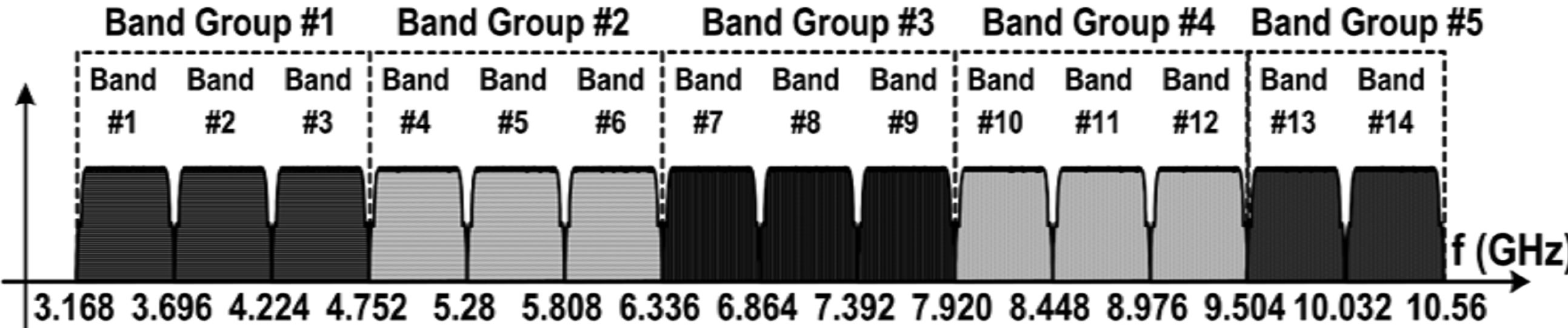 (b)
(b)
Figure 1. Spectrum allocated for UWB communication. (a) DS-CDMA; (b) MB-OFDM.
notch filtering function. In the first step, we design the UWB amplifying circuit. In the second step, the notch filter is added properly. The input impedance, noise, gain and notch filter of UWB LNAs are discussed in Section 2. Section 3 presents the final schematic of the proposed LNA. Finally, the measurements and simulation results of the UWB LNA are discussed in Section 4, which is followed by conclusions in Section 5.
2. LNA Design Technique
2.1. Input Impedance Matching of Common Gate Amplifier
In the design of LNAs for broadband wireless receivers, there are several issues that need to be investigated. These include low and stable 50 Ω input matching, flat gain with sufficient linearity, NF of the amplifier, and low power consumption, which is needed in portable systems. In this section, input impedance matching, noise analysis, and gain analysis for broadband LNA development is discussed.
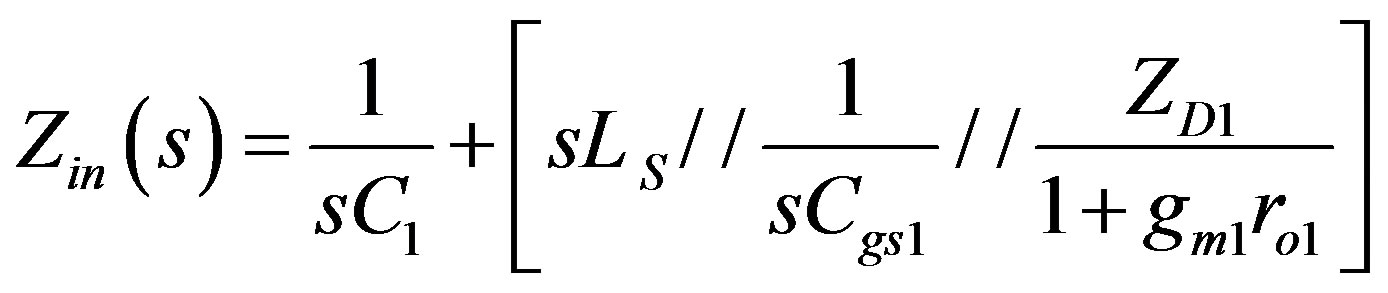
Figure 2 shows the circuit with input stage of a common-gate amplifier. The inductor LS is placed between the source of the MOS transistor and the ground terminal forming an LC resonator with the gate-to-source capacitance Cgs in a common-gate configuration [4]. The finite output resistance of the transistor also changes the input reflection of the LNA. In Figure 2, the load impedance of the common-gate stage and input impedance of the next stage will affect the matching and noise contribution due to the short-channel MOS transistor’s relatively low output resistance which is about 500 Ω for a 0.18 μm CMOS process [6]. The small-signal equivalent circuit for the impedance calculation is shown in Figure 3. From Figure 3, the input impedance can be derived as
 (1)
(1)
Note that gm1 is the small signal transconductance of the transistor M1, and that ZD1 and ZD2 are given by Equations (2) and (3), respectively.
 (2)
(2)
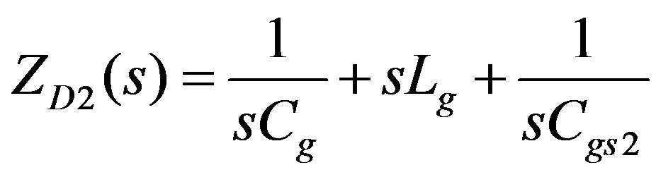 (3)
(3)
In the process of the derivation, ZD2 is indicated as the input impedance of the transistor M2 amplifier with resistor R1 feedback loop. And ZD1 is the total impedance
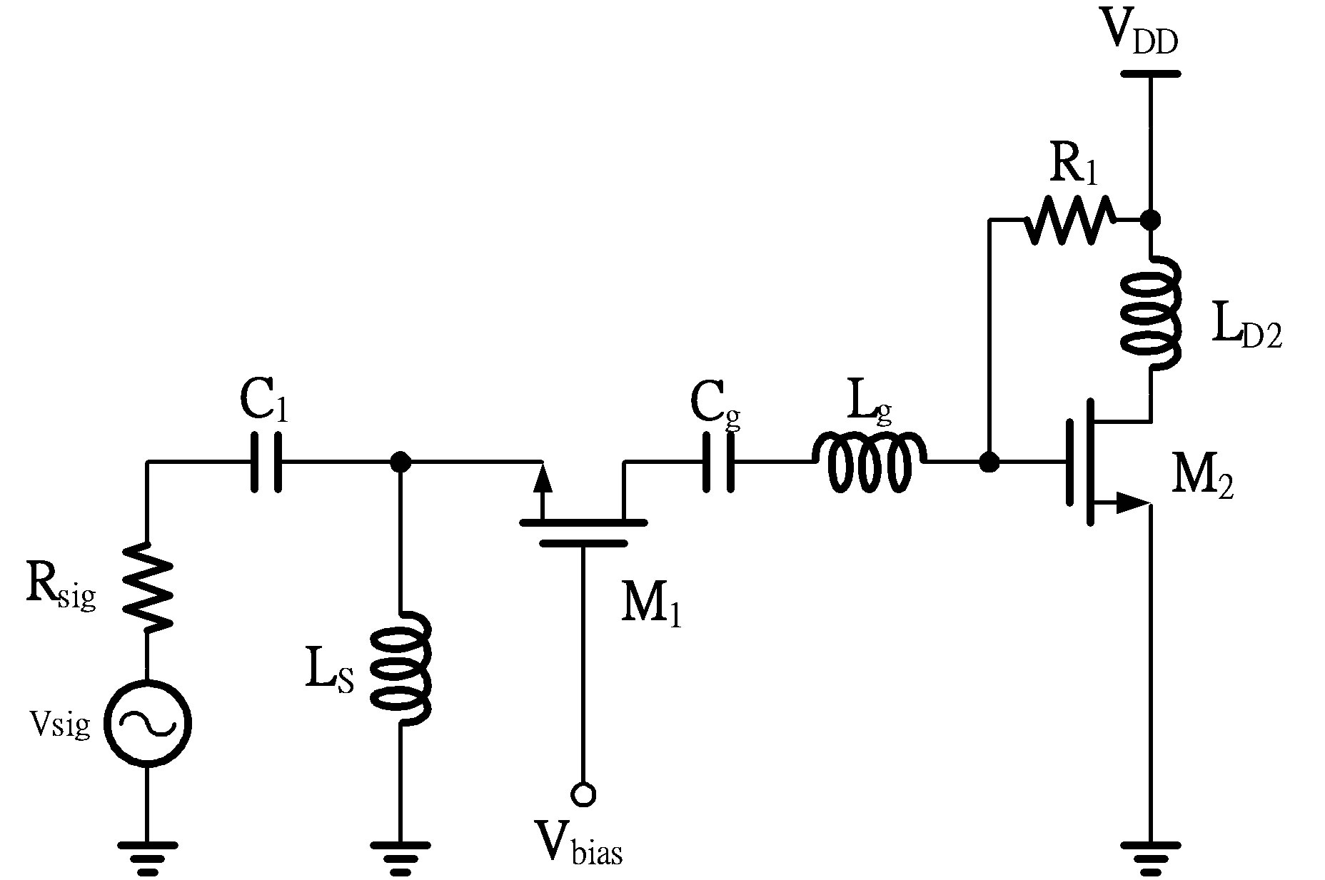
Figure 2. Configuration of a common-gate input stage.

Figure 3. Small-signal equivalent circuit of a common-gate CMOS amplifier.
looking into the drain terminal of transistor M1.
If we set , then Re(Zin) is the real part resistance for 50Ω source signal matching, and Im(Zin) is the imaginary part for resonance frequency tuning.
2.2. Noise Analysis
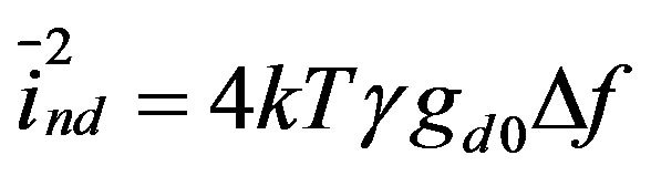
To analyze the noise characteristics of the CGLNA, the noise sources are added to the small-signal equivalent circuit as shown in Figure 4.  represents the meansquare drain noise current which is given by [5-8]
 (4)
(4)
where k is the Boltzmann constant, T is the absolute temperature in Kelvin, gd0 is the zero-bias drain conductance, and Δf is the noise bandwidth in hertz over which the measurement is made. The parameter γ is a bias-dependent factor. For long-channel devices, γ has the value of unity at zero VDS and 2/3 at saturation. For shortchannel devices, the value of γ can be more than 2, depending on the bias conditions. The induced gate noise current  is given by [5-8]
 (5)
(5)
where δ is the gate noise coefficient of which the typical value is 4/3 for long-channel devices. Note that gg is given by
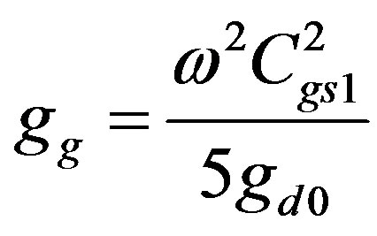 (6)
(6)
Due to the low gain of the common-gate stage, the noise contribution of the second stage cannot be neglected. The total noise factor of a two-stage amplifier can be expressed as follows [4]
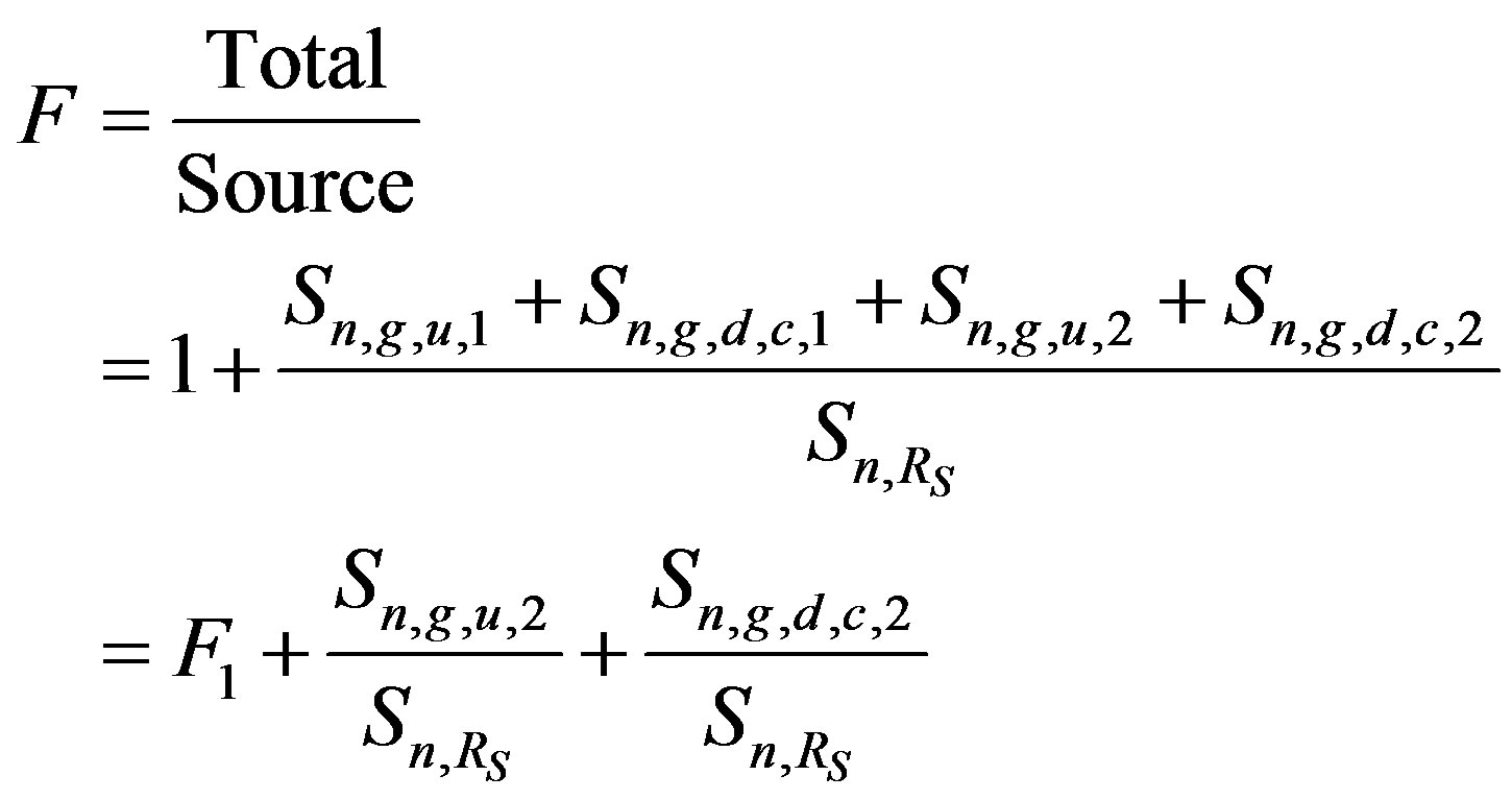 (7)
(7)
where F1 is the noise factor of the single common-gate stage, excluding the effect of the noise contributed by the

Figure 4. Noise model for the amplifying transistor.
common source-stage which is given by the later two terms. F1 is given by
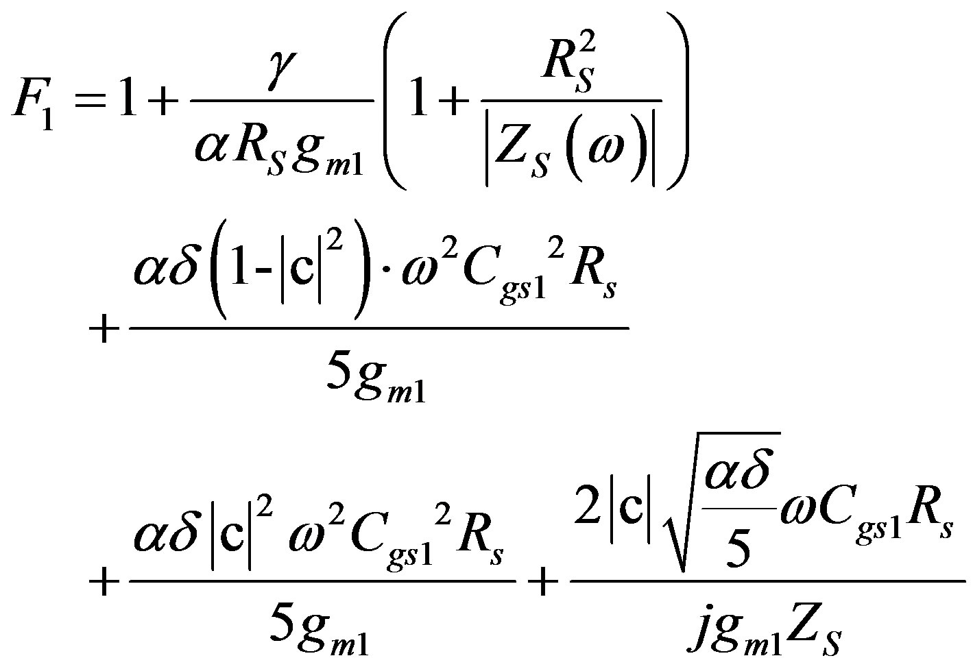 (8)
(8)
where 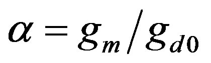 and |c| is a correlation coefficient with predicted value of 0.395 [9-11].
According to Equation (8), the drain noise is based on our circuit when considering Equation (4). The correlation between input and output noise is about 0.68 - 0.85, which is dependent on bias voltage. The total noise contribution is dominated by gm1 in the denominators; we can increase it to reduce the overall noise. However, the input matching degrades as gm1 increases. By properly choosing the device parameter to satisfy simultaneous gain and noise matching, we can sacrifice a little S11 to reduce the noise contribution.
2.3. Gain Analysis (Compensation)
In order to reduce supply voltage and power consumption while providing sufficient gain at multigigahertz frequencies, a complementary amplifier with a currentreused circuit topology is employed [11-14]. Because of the corresponding gain, performance is usually not high enough for UWB application due to the tradeoff between gain and bandwidth [15,16]. The presented LNA adopts two-stage cascade architecture to achieve enough power gain and bandwidth. The first stage is designed to resonate at the lower band, and the second stage is to resonate at the higher band. In order to achieve a flatness power gain, the inter-stage matching network is designed for gain compensation. The behavior of gain compensation is illustrated in Figure 5" target="_self"> Figure 5.
2.4. Notch Filter
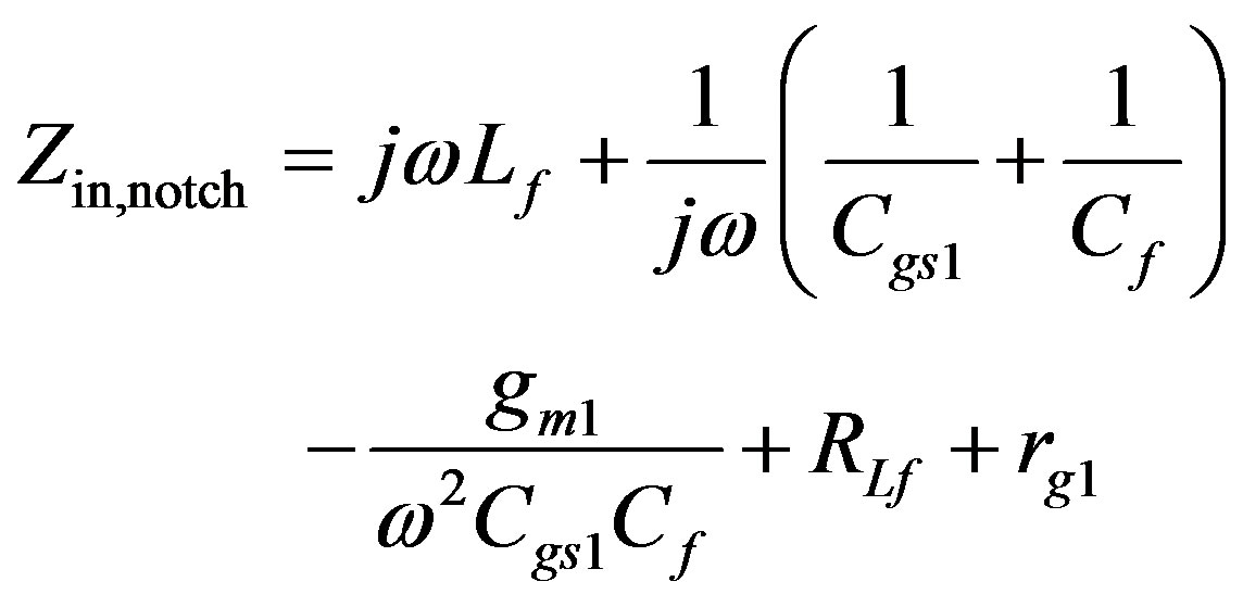
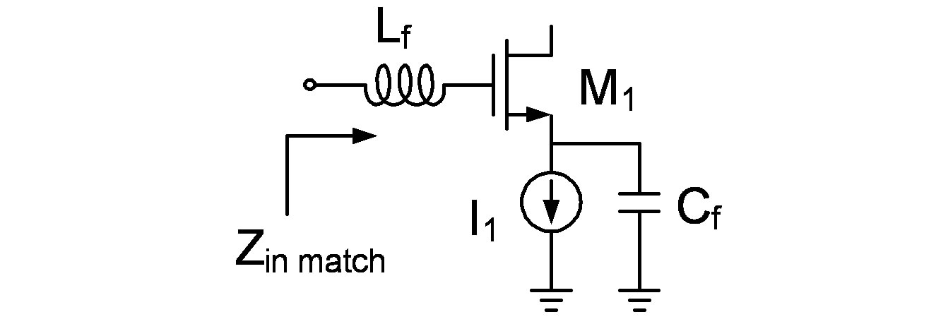
Recently, some researchers have reported on LNA with notch filters [17-22]. Figure 6(a) shows an active second-order notch filter and a small signal equivalent circuit is shown in Figure 6(b). From Figure 6(b), the input impedance of the filter is given by [18]
 (9)
(9)
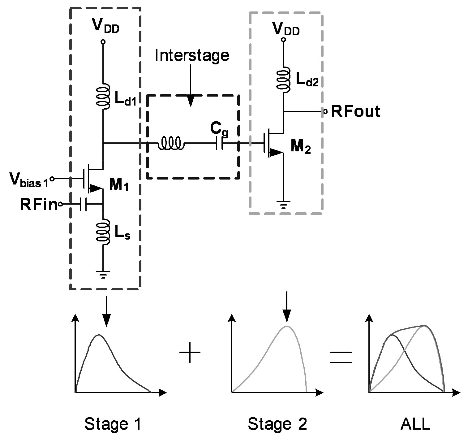
Figure 5. Two-stage amplifiers with the behavior of gain compensation.
 (a)
(a)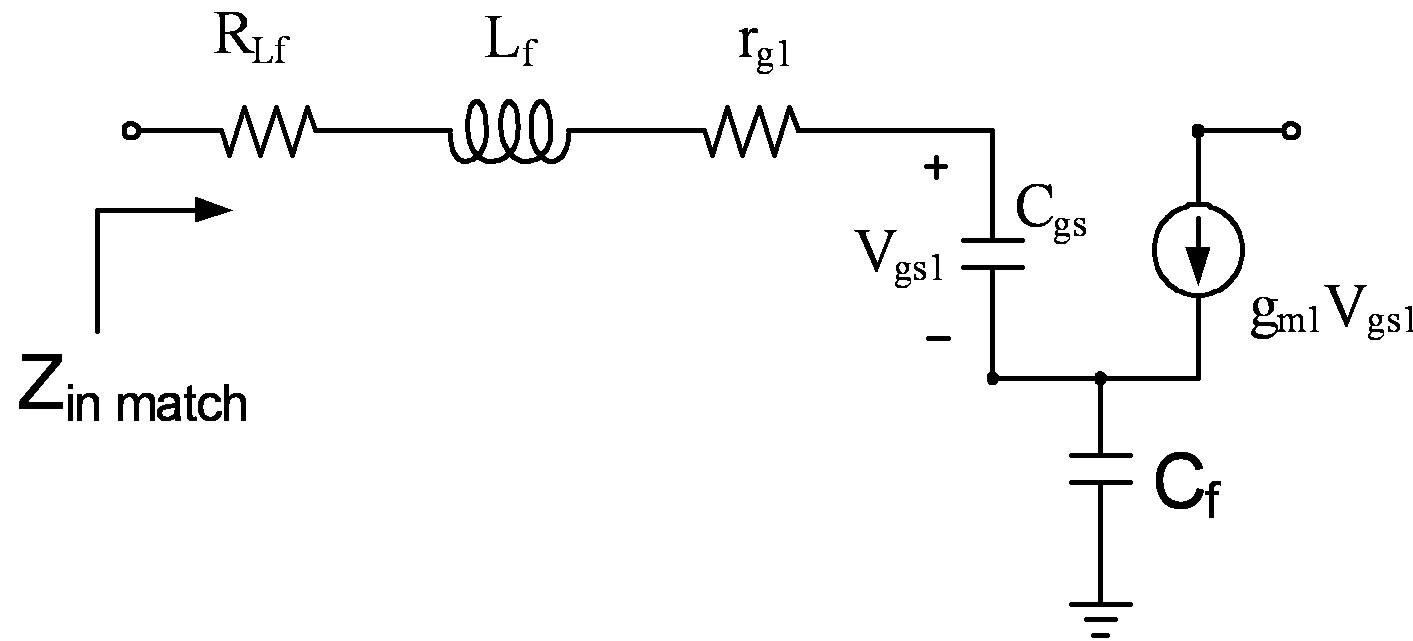 (b)
(b)
Figure 6. (a) Schematic of the second-order active notch filter; (b) The small signal equivalent circuit.
where rg1 is the series gate resistance of M1, and RLF is the series resistance of on-chip inductor Lf.
Note that the negative term on the Equation (9) represents the negative resistance seen at the gate of transistor M1 which is proportional to gm1. RL1 and rg1 can be cancelled by a suitable negative value hence leaving the imaginary impedance. Though the negative resistance comes from the notch filter, its purpose is to function as the deep rejection ratio. Therefore, the stability of the UWB amplifying circuit does not matter.
Therefore, the quality factor of the on-chip integrated inductor plays a minor role in the quality factor of the filter, which can be obtained as
 (10)
(10)
where gm1 is large enough to cancel the denominator, and where the Q-factor of the notch filter becomes infinity. Thus, a very deep rejection ratio is obtained. The rejection frequency can be derived as
 (11)
(11)
From the 802.11a WLAN system, the major interference sources are the in-band signal which occupies at the 5 - 6 GHz band, so the frequency of notch filter fnotch which is set to be 5.5 GHz. As can be seen from Figure 7, the image signal at 5.5 GHz is very low, while the impedance at the wanted signal has a peak value.
3. Final Proposed LNA Circuit
The fully integrated UWB LNA with current-reused and notch filter topology is implemented in the TSMC 0.18 μm CMOS process. The schematic of this circuit including the output buffer is shown in Figure 8. In this circuit, both M1 and M2 operate as common-source stages, but they share the same bias current. The signal amplified by M1 is coupled to the gate of M2 by C1 while the source of M2 is bypassed by C2. The circuit thus saves power through the reuse of the bias current [14]. To elevate the bandwidth of the CMOS LNA close to 3.1 - 10.6 GHz, a two-stage configuration with band extension inductor Ls is adopted. The input common-gate stage not only provides wideband input matching, but also a narrow-band frequency at lower frequency. The spiral inductor Ls is chosen with a relatively high Q factor, and resonates with Cgs of M1 around the center of the 3.1 to 10.6 GHz band. The second stage of the common source amplifier with inductive load Ld2 provides high-frequency gain and determines higher frequency of the LNA. To achieve the goal of low power operation, the second stage is stacked on top of the first stage. The inter-stage matching network consists of Lg and Cg, which is to maintain gain
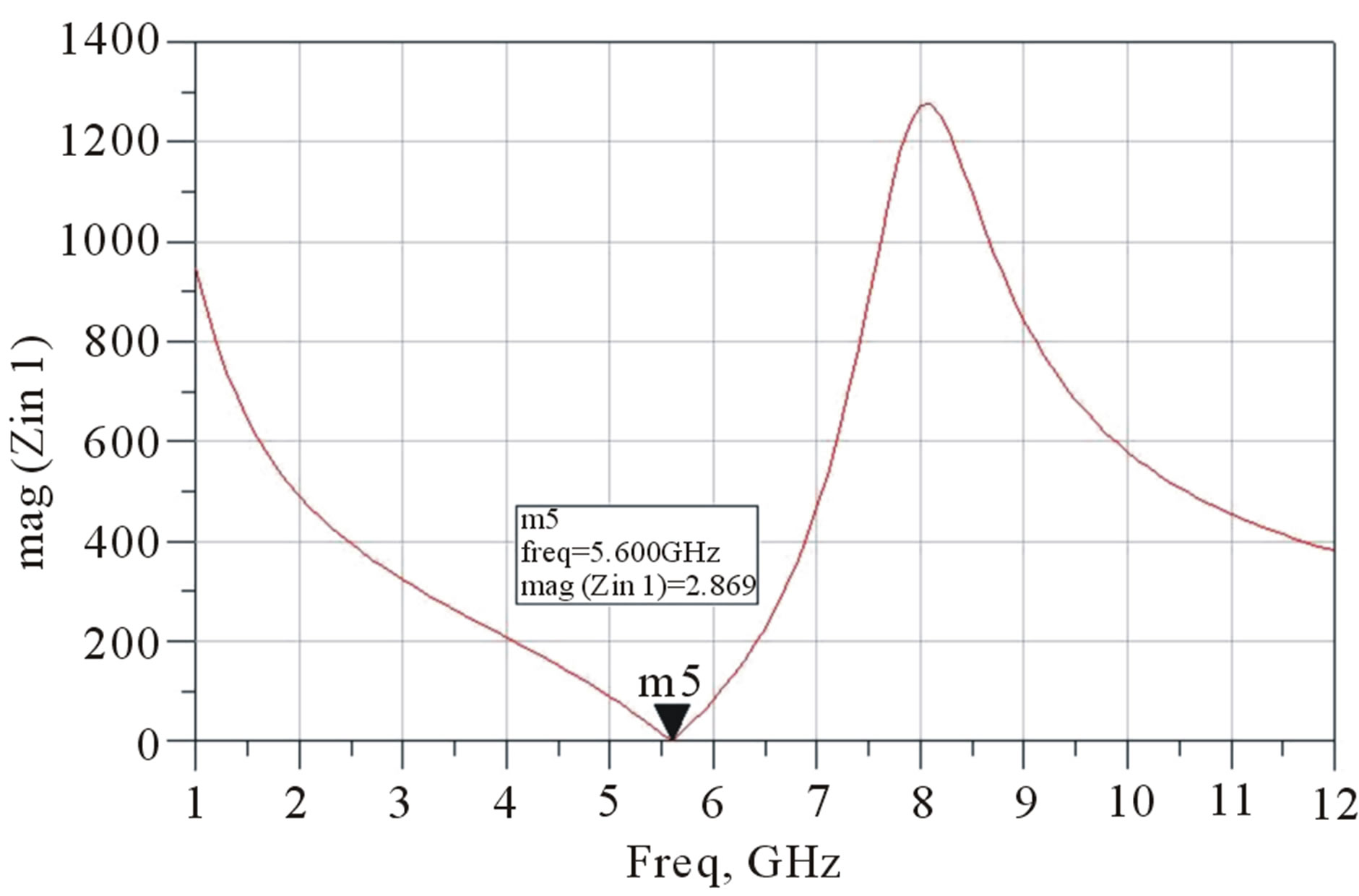
Figure 7. Filter characteristic of the proposed notch filter.
flatness. The M6 transistor with bias in Figure 8 is tuned as a current source I1 in Figure 6.
The series inductor Lb further resonates with the input capacitance of M3, resulting in a large bandwidth and some residual peaking on the frequency response. Figure 9 shows the bandwidth improvement for practical Lb value.
The bypass capacitor C2 provides an ac ground path for the second stage and avoids the coupling to the first stage. A source follower stage has been added as an output buffer for measurement purposes. The branch current in the proposed circuit with ID1, ID2 and ID3 is 2.76 mA, 2.27 mA and 0.88 mA, respectively. ID1 indicates the current of the first stage with current-reused topology, ID2 indicates the current of the output stage, and ID3 indicates the current of the notch filter circuit. Devices sizes are summarized in Table 1" target="_self"> Table 1.
4. Measurement Results
The chip microphotograph of the fully integrated UWB
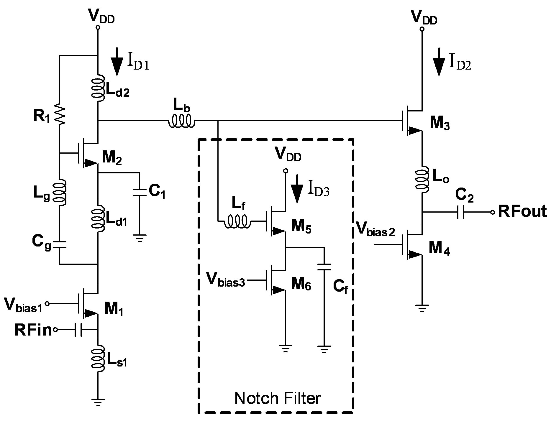
Figure 8. Proposed circuit for UWB system.
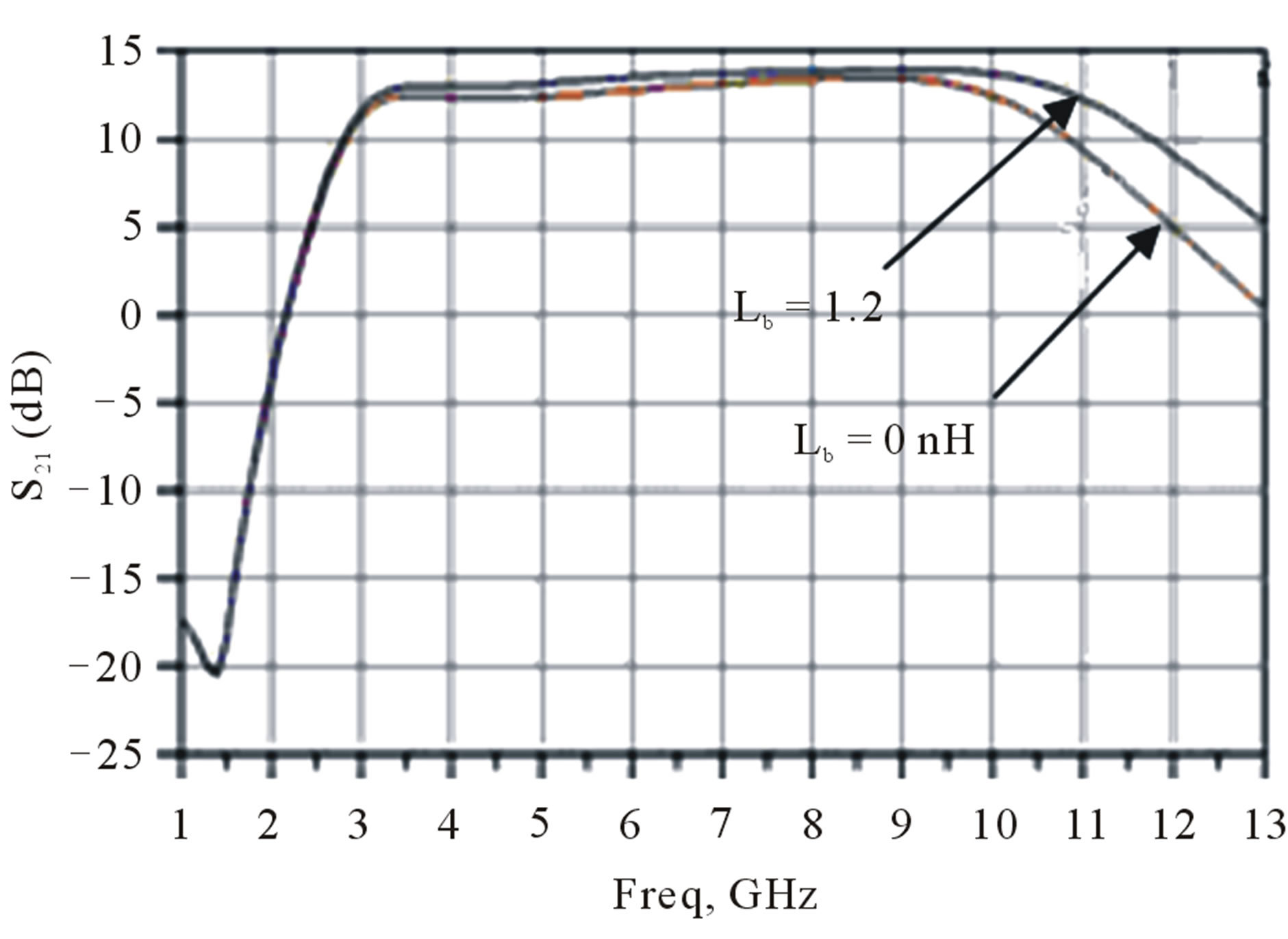
Figure 9. The bandwidth improvement of the gain performance.
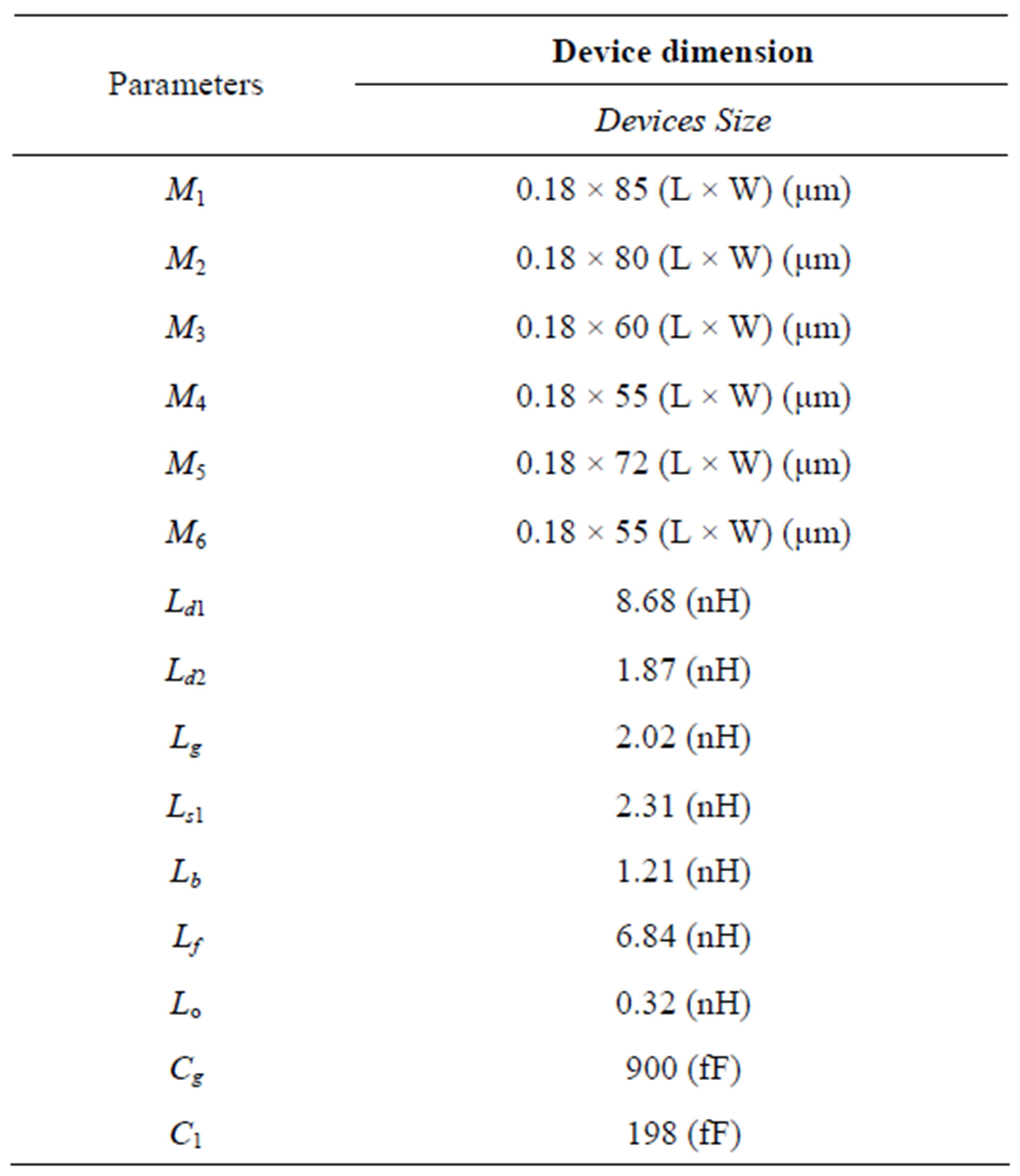
Table 1. Device dimension.
LNA is shown in Figure 10. The area of the circuit including testing pads occupies approximately 1.26 mm2. The total power consumption of the proposed LNA including the output buffer is only 6.4 mW under 1-V supply voltage. Figures 11 and 12 show the measured and simulated input and output reflection coefficients.
The S11 and S22 are both below –10 dB over the entire 3 - 10 GHz band. The difference with the 1 GHz frequency shift between simulation and measurement is caused by the variation of parameters and pad coupling capacitance of the measuring process.
The measured and simulated power gain of the LNA is shown in Figure 13. In the 3 - 5 GHz band, the measured peak gain is 15 dB at 3.1 GHz while in the 6 - 12 GHz band the peak gain is 11 dB at 11.6 GHz. The high band has gained variation with about 3 - 4 dB between the simulation and measurement. The original frequency of the notch filter is designed at 5.5 GHz. The results come from the parasitic quality of the notch filter, especially caused by the input capacitive property of transistors M5 and M6. Owing to the variation of capacitance, the location of the frequency also shifted forward. Therefore, the center frequency of the notch band is tuned to 4.8 GHz with a minimum rejection gain of –9.7 dB. Figure 14 shows the measured and simulated noise figures of the LNA.
The measured minimum noise figure is about 5 dB around 4 GHz. The difference of average noise figures between the measurement and simulation is about 2 dB below 8 GHz. This extra noise arose from the process
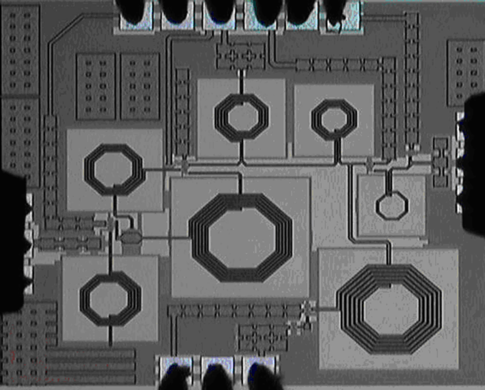
Figure 10. Microphotograph of the CMOS LNA chip.
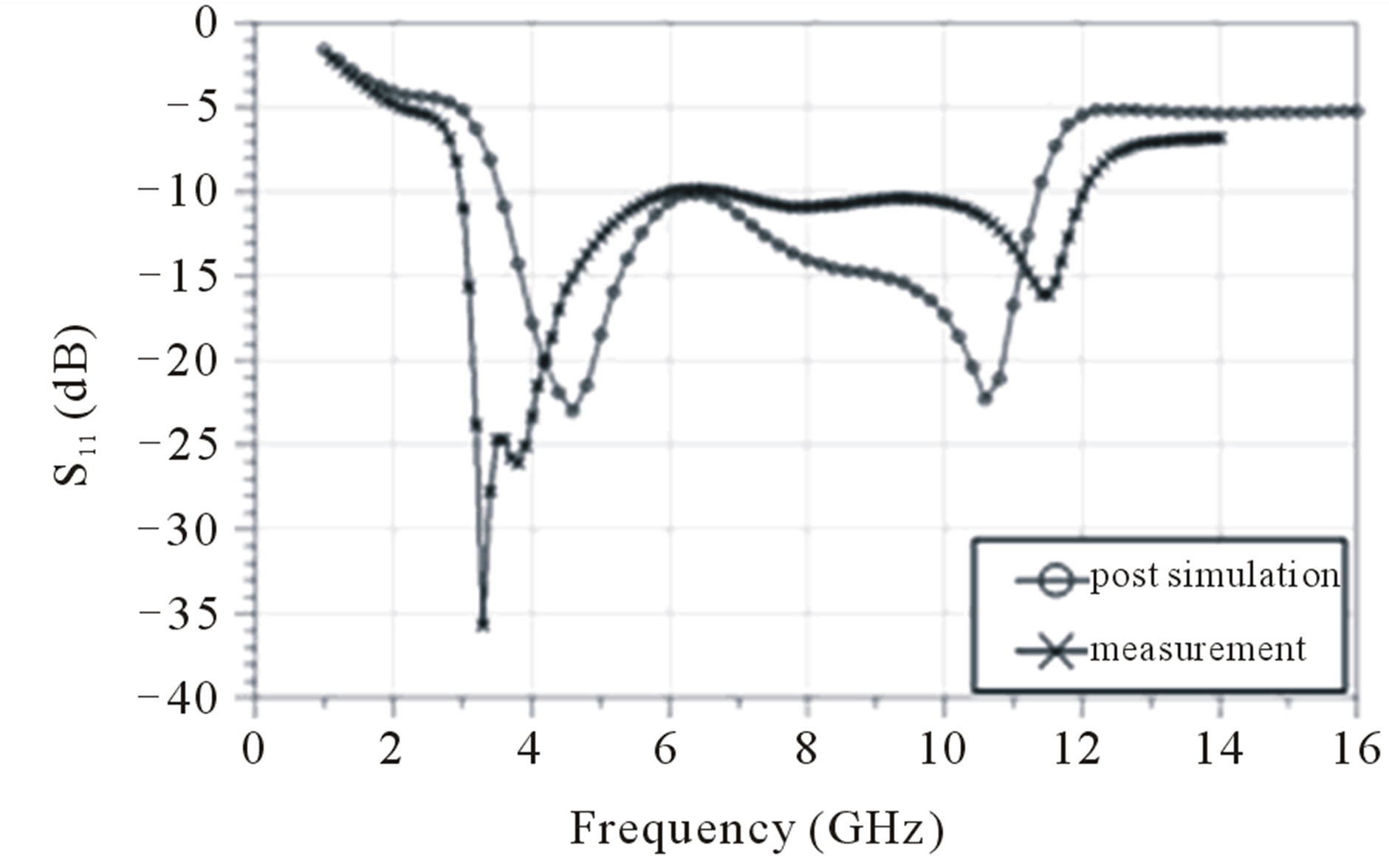
Figure 11. Measured and simulated input returns loss.
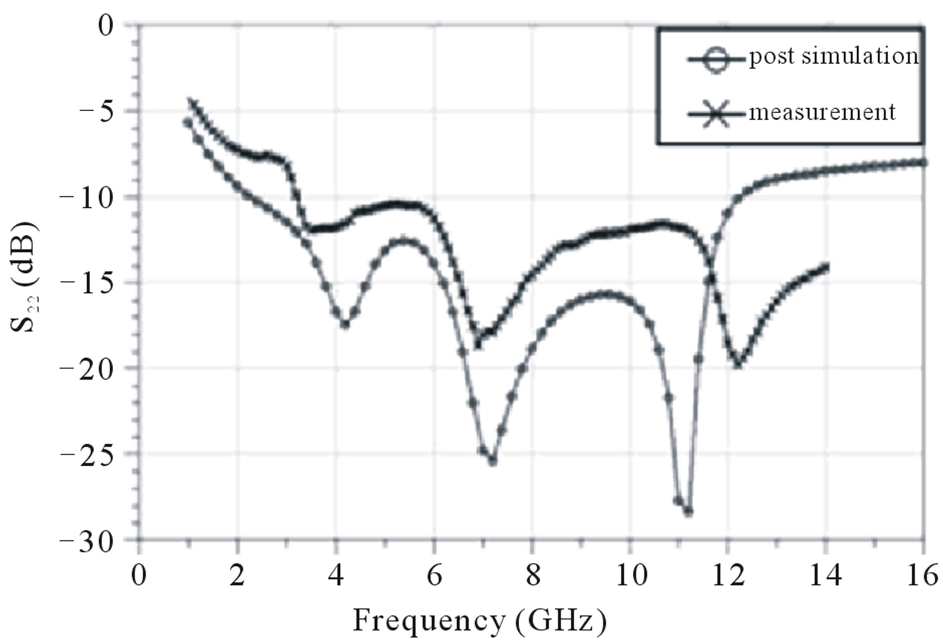
Figure 12. Measured and simulated output returns losses.
variation of the device and the structure of the common-gate LNA circuit. The high NF in the 5.5 GHz zone will slightly affect the signal transmission of system performance. A two-tone test with 10 MHz tone separation was performed to measure the third-order intermodulation distortion (IMD3). Figure 15 shows that the measured input third-order intercept point (IIP3) at 6 GHz is
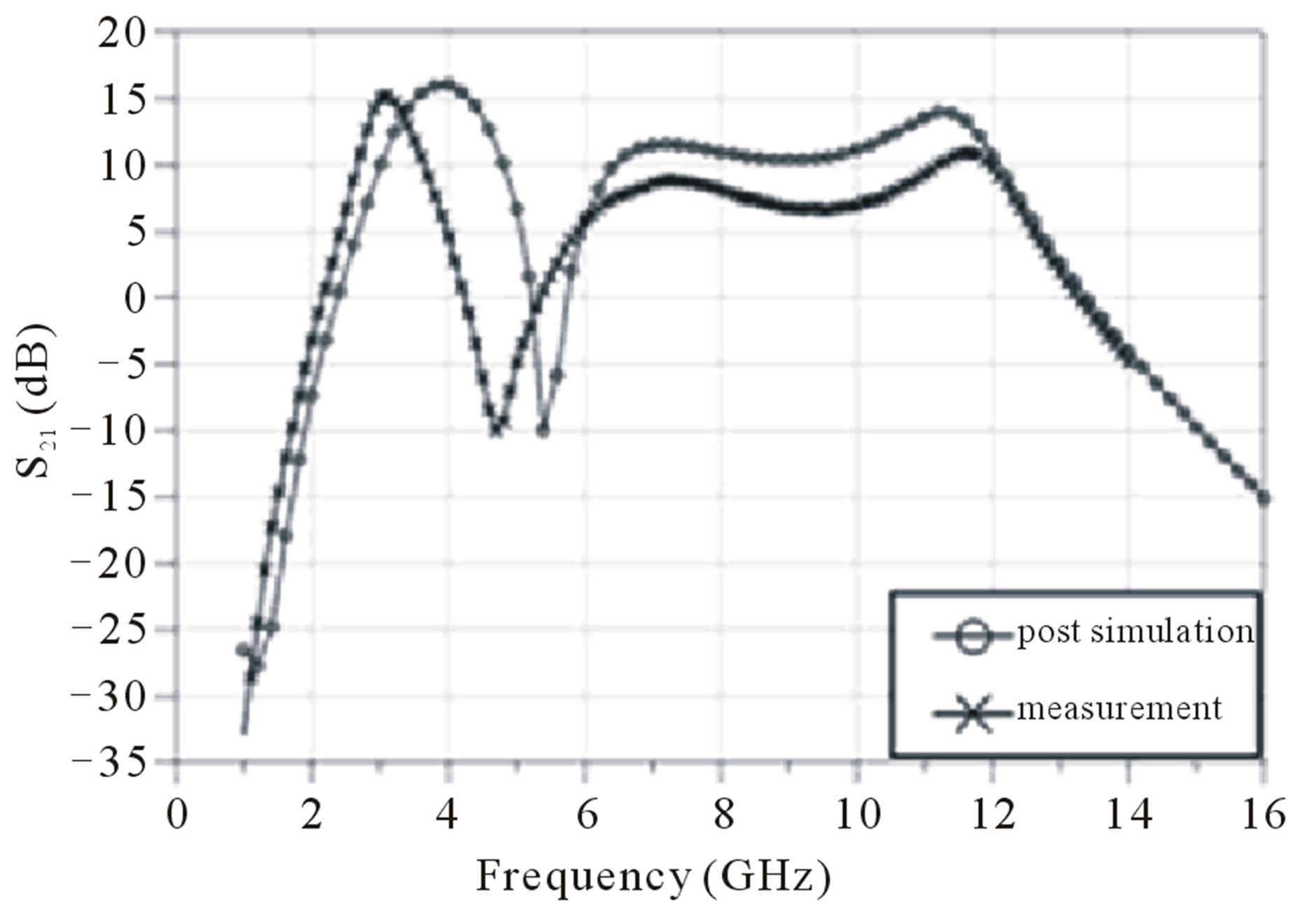
Figure 13. Measured and siumlated gain of the CMOS LNA.
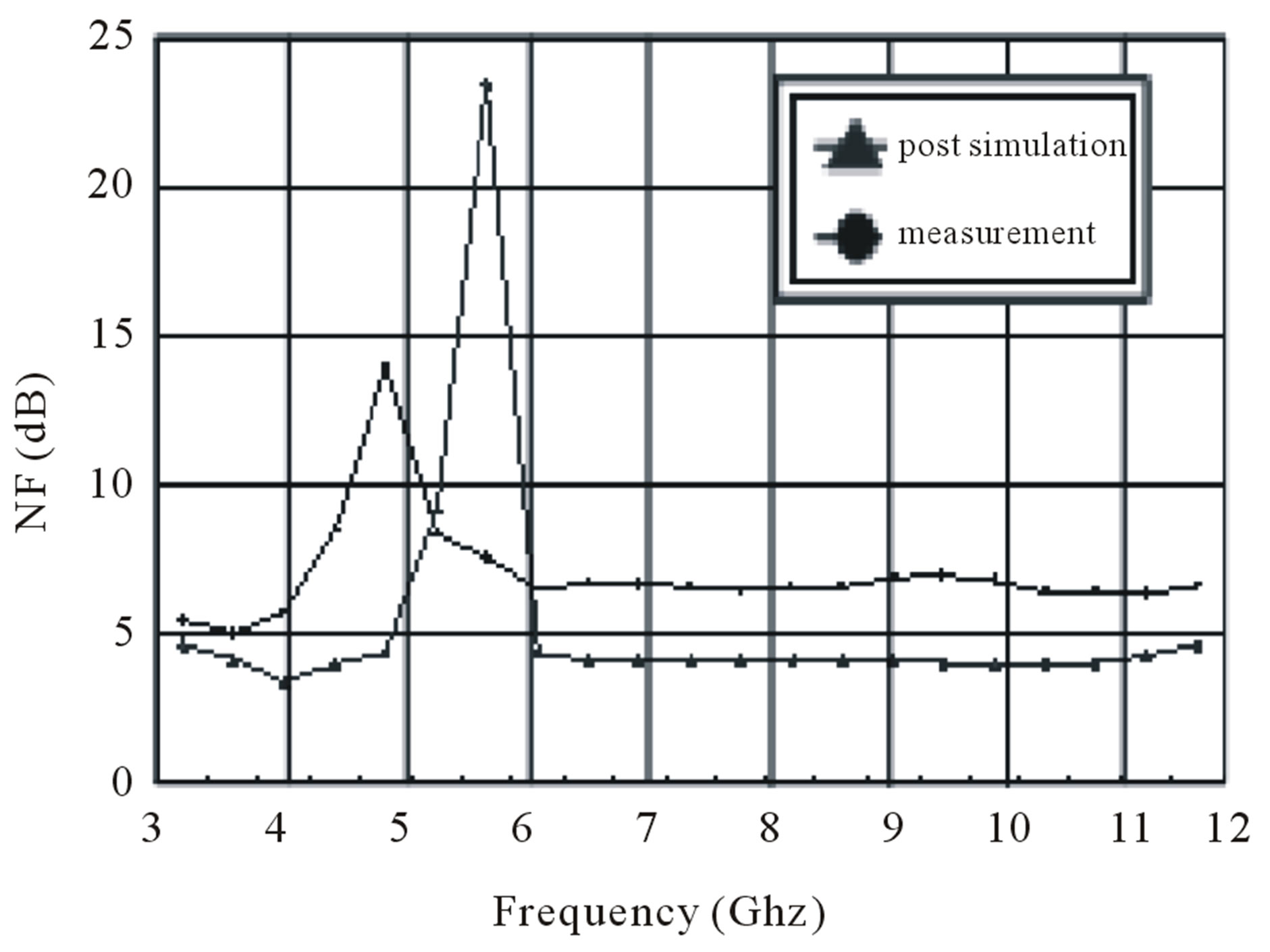
Figure 14. Measured and simulated noise figures.
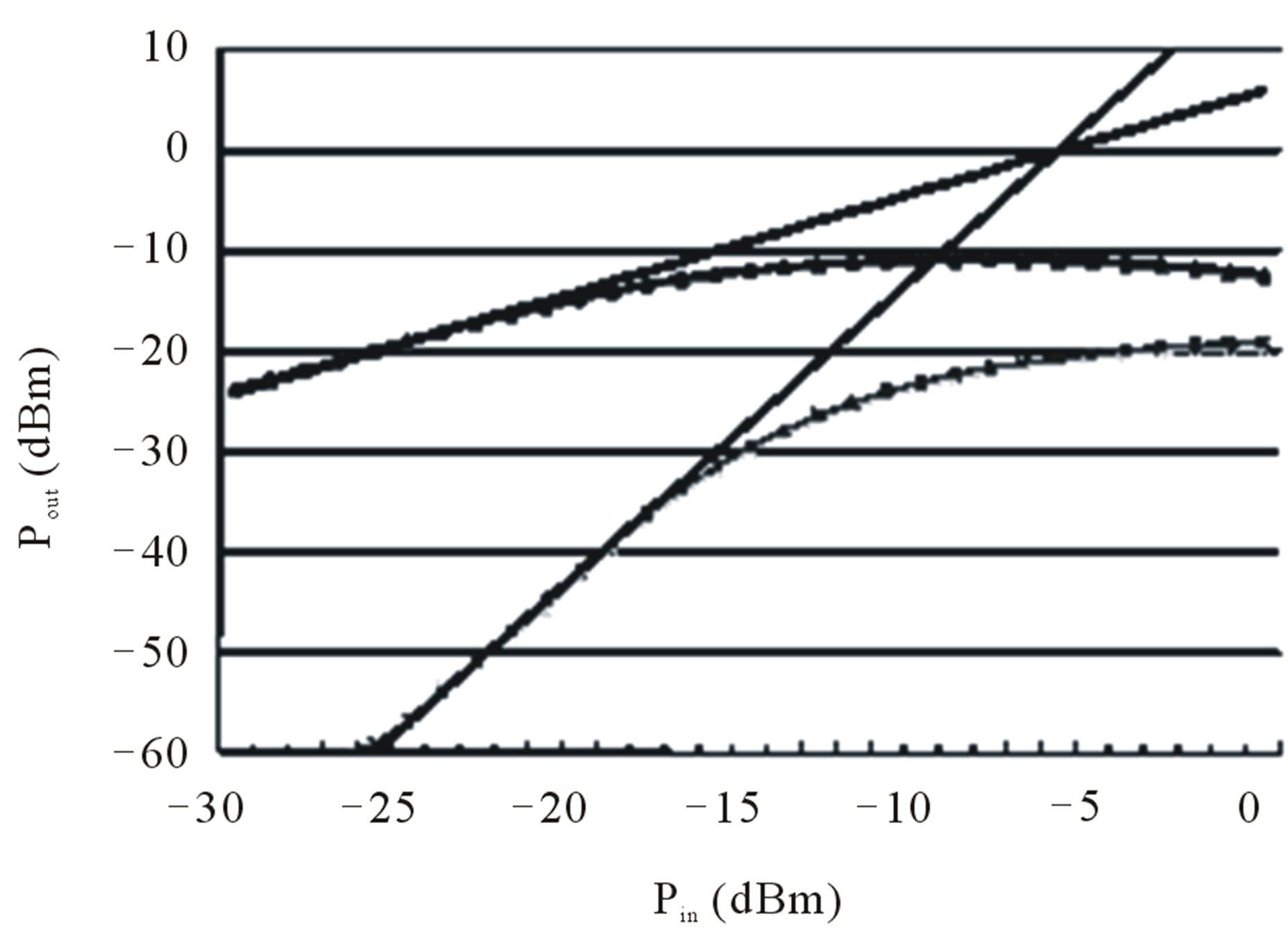
Figure 15. Measured input IIP3 at 6GHz.
–7 dBm.
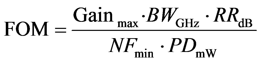
A figure-of-merit (FOM) is proposed to characterize the overall performance of the UWB LNA and evaluate the effectiveness of the design methodology as follows [21]:
 (12)
(12)
where Gain is maximum power gain, BW is bandwidth, NF is the minimum noise figure and RR indicates the rejection ratio. Generally, gain variation is not considered in notch filter; yet in this design, Gainmax, bandwidth, noisemin, power consumption and rejection ratios are considered in the FOM.
A summary of the rest of the measurements is also included in Table 2" target="_self"> Table 2. The performance comparison with other reported papers is shown in Table 3. The rejection gained more than 20 dB in Table 3 which is nearly the lowest because of the larger variation of the ripple with gain flatness. Compared with these amplifiers, this work achieves the highest FOM and the lowest power consumption of 6.4 mW.
5. Conclusion
A low power LNA with notch filter intended for 4.8 GHz
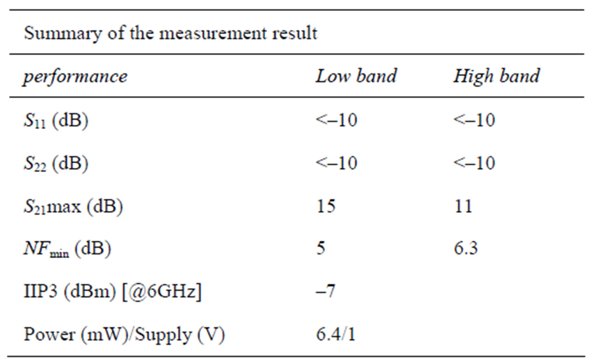
Table 2. Summary of the measurement result.
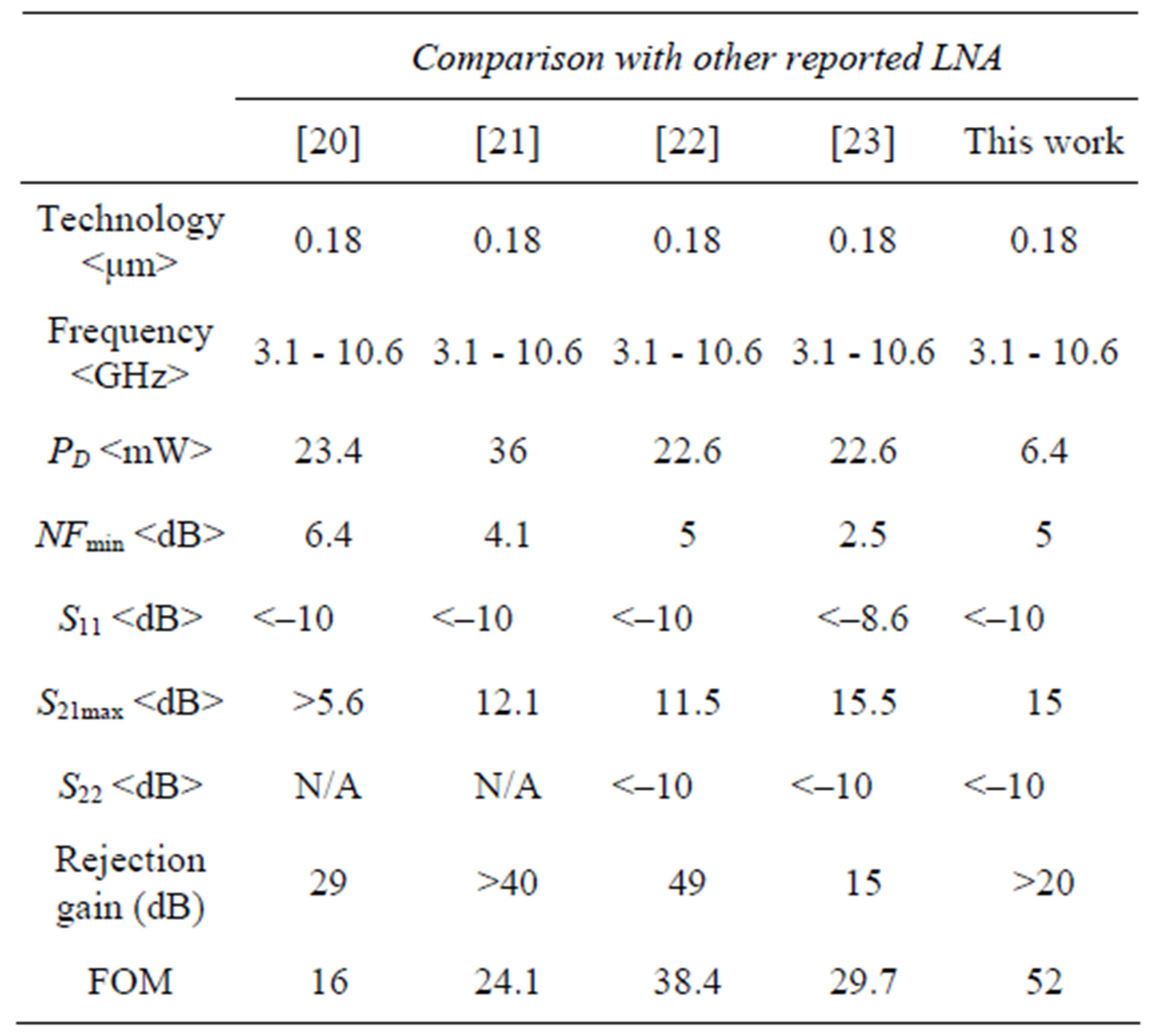
Table 3. Comparison with other reported LNA.
interference rejection in UWB systems has been presented in this paper. The proposed common-gate is employed to achieve wideband input matching with low noise and very low power consumption using a stagger tuning technique and current reused architecture. The power consumption is 6.4 mW with 1 V supply voltage. From 3.1 to 10.6 GHz, the power gain is higher than 15 dB and the minimum noise figure is 5 dB. The deepest rejection ratio that can be attained is –10 dB.
6. Acknowledgements
The authors wish to thank the Chip Implementation Center (CIC) of the Nation Science Council, Taiwan, for supporting the TSMC CMOS process and further fabrication. This work has been supported by National Yunlin University of Science & Technology with 97T13.
REFERENCES
- S. Stroh, “Ultra-Wideband: Multimidea Unplugged,” IEEE Spectrum, Vol. 40, No. 9, 2003, pp. 23-27. doi:10.1109/MSPEC.2003.1228004
- R.-C. Liu, K.-L. Deng and H. Wang, “A 0.6-22-GHz Broadband CMOS Distributed Amplifier,” IEEE Radio, 8-10 June 2003, pp. 103-106.
- A. Bevilacqua and A. M. Niknejad, “An Ultrawideband CMOS Low-Noise Amplifier for 3.1-10.6-GHz Wireless Receivers,” IEEE Journal of Solid-State Circuits, Vol. 39, No. 12, 2004, pp. 2259-2268. doi:10.1109/JSSC.2004.836338
- L. Yang, Y. Kiat Seng, A. Cabuk, M. Jianguo, D. Manh Anh and L. Zhenghao, “A Novel CMOS Low-Noise Amplifier Design for 3.1 to 10.6-GHz Ultra-Wide-Band Wireless Receivers,” IEEE Transactions on Circuits and Systems, Vol. 53, No. 8, 2006, pp. 1683-1692. doi:10.1109/TCSI.2006.879059
- C.-H. Chen, M. J. Deen, Y. Cheng and M. Matloubian, “Extraction of the Induced Gate Noise, Channel Noise, and Their Correlation in Submicron MOSFETs from RF Noise Measurements,” IEEE Transactions on Electron Devices, Vol. 48, No. 12, 2001, pp. 2884-2892. doi:10.1109/16.974722
- B. Razavi, “Design of Analog CMOS Integrated Circuits,” McGraw-Hall, Boston, 2001.
- T. H. Lee, “The Design of CMOS Radio-Frequency Integrated Circuit,” 2nd Edition, Cambridge Press, Cambridge, 2004.
- A. van der Ziel, “Noise in Solid-State Devices and Circuits,” John Willey and Sons, New York, 1986.
- D. K. Shaeffer and T. H. Lee, “A 1.5-V, 1.5-GHz CMOS Low Noise Amplifier,” IEEE Journal of Solid-State, Vol. 32, No. 5, 1997, pp. 745-759. doi:10.1109/4.568846
- M.-T. Hsu and K.-J. Li, “An Ultrawideband CMOS Low Noise Amplifier for 3.1-10.6 GHz Wire Less Communication,” ICUWB 2007, Singapore City, 24-26 September 2007, pp. 457-460.
- B. Razavi, “RF Microelectronics,” Prentic-Hall, Eglewood Cliffs, 1998.
- Y.-J. Lin, S. S. H. Hsu, J.-D. Jin and C. Y. Chan, “A 3.1 - 10.6 GHz Ultra-Wideband CMOS Low Noise Amplifier with Current-Reused Technique,” IEEE Microwave and Wireless Components Letters, Vol. 17, No. 3, 2007, pp. 232-234. doi:10.1109/LMWC.2006.890503
- Z.-Y. Huang, C.-C. Huang, Y.-T. Hung and M.-P. Chen, “A CMOS Current Reused Low-Noise Amplifier for Ultra-Wideband Wireless Receiver,” International Conference on Microwave and Millimeter Wave Technology, Chengdu, 19-21 November 2008, pp. 1499-1502. doi:10.1109/ICMMT.2008.4540731
- H. L. Kao, A. Chin, K. C. Chang and S. P. McAlister, “A Low-Power Current-Reuse LNA for Ultra-Wideband Wireless Receivers from 3.1 to 10.6 GHz,” Topical Meeting on Solid-State Circuits, Silicon Monolithic Integrated Circuits in RF Systems, Long Beach, 10-12 January 2007.
- S. Shekhar, X. Li and D. J. Allstot, “A CMOS 3.1 - 10.6 GHz UWB LNA Employing Stagger-Compensated Series Peaking,” IEEE RFIC Symposium, San Francisco, 11-13 June 2006, pp. 49-52.
- C.-P. Liang, P.-Z. Rao, T.-J. Huang and S.-J. Chung, “Analysis and Design of Two Low-Power Ultra-Wideband CMOS Low-Noise Amplifiers with Out-Band Rejection,” IEEE Transactions on Microwave Theory and Techniques, Vol. 58, No. 2, 2010, pp. 277-286. doi:10.1109/TMTT.2009.2037855
- A. Vallese, A. Bevilacqua, C. Sandner, M. Tiebout, A. Gerosa and A., Neviani, “Analysis and Design of an Integrated Notch Filter for the Rejection of Interference in UWB Systems,” IEEE Journal of Solid-State Circuits, Vol. 44, No. 2, 2009, pp. 331-343. doi:10.1109/JSSC.2008.2010984
- T.-K. Nguyen, N.-J. Oh, C.-Y. Cha, Y.-H. Oh, G.-J. Ihm and S.-G. Lee, “Image-Rejection CMOS Low-Noise Amplifier Design Optimization Techniques,” IEEE Transactions on Microwave Theory and Techniques, Vol. 53, No. 2, 2005, pp. 538-547. doi:10.1109/TMTT.2004.840744
- P. Bi and D. Anh, “Dual-Mode Tunable Q-Enhanced Filter for Narrowband and UWB Systems,” Canadian Conference on Electrical and Computer Engineering, Ottawa, 7-10 May 2006, pp. 2318-2321.
- A. T. Kenneth, B. Leonid, W. H. James and N. Jonh, “Ultra Wideband Front-End with Tunable Notch Filter,” IEEE North-East Workshop on Circuits and Systems, Gatineau, 18-21 June 2006, pp. 177-180.
- R.-M. Weng, R.-C. Kuo and P.-C. Lin, “An Ultra-Wideband LNA with Notch Filter,” 17th International Conference Radioelektronika, Brno, 24-25 April 2007. doi:10.1109/RADIOELEK.2007.371431
- C.-C. Huang, Z.-Y. Huang, Y.-C. Wang, Y.-T. Huan and M.-P, Chen, “0.18 μm CMOS Low-Noise Amplifier with 2nd-Order Notch Filter for Ultra-Wideband Wireless Receiver,” IEEE International Workshop on Radio-Frequency Integrated Technology, Singapore City, 9-11 December 2007.
- J. Asmussen, S. P. Sah, X. M. Yu and D. Heo, “A Wideband Body Biased Low-Noise Amplifier,” International Conference on Green Circuits and Systems, Shanghai, 21-23 June 2010, pp. 687-690.