Wireless Engineering and Technology
Vol.2 No.2(2011), Article ID:4548,5 pages DOI:10.4236/wet.2011.22014
Layout Design of LC VCO with Current Mirror Using 0.18 um Technology
![]()
Department of Electronics & Instrumentation Engineering, Shri G. S. Institute of Technology and Science, Indore, India.
Email: {rsgamad, namrata.prasad7}@gmail.com
Received October 1st, 2010; revised February 26th, 2011; accepted February 28th, 2011.
Keywords: VCO, LC-tank, Low phase noise, Low power consumption, tuning range, spiral inductor
ABSTRACT
This paper presents a new design of complementary oxide semiconductor voltage controlled oscillator (CMOS VCO) for improve tuning range and phase noise with low power consumption. Design is area efficient and easy to implement. Design is carried out in cadence and schematic editor using 180 nm technology. Simulation is done and performance results are reported. Results have been compared with earlier published work and improvements are obtained in this work.
1. Introduction
Today is increasing demand for wireless and multimedia applications keeps pushing the CMOS integrated wireless systems to support much communication standards (WLAN, GSM, UWB and DVB etc) [1]. As gigahertzband communication is becoming more mature, the realization of a single chip transceiver becomes more demanding, with the need for lower cost, reduced size and less power consumption. As for the local oscillator signal generated from the integrated frequency synthesizer, the transceivers matched these standards need excellent phase noise performance and wide tuning range solving the frequency offset due to the variations of process, temperature and voltage [2]. So, CMOS voltage-controlled oscillator (VCO) will be challenging RF block. Especially, the higher close in phase noise due to higher 1/f noise in CMOS continues to be a challenge. As per demand for multi-band and multi-standard radios requires VCO’s operating over a wider frequency range. Wireless standards specify the minimum level of the received signal, the maximum level of noise, the channel bandwidth, and the spacing between adjacent channels. Therefore, the maximum amount of acceptable phase noise on the oscillator can be calculated using the required signal to noise ratio after down conversion [3,4]. This paper presents a novel VCO architecture that can achieve low phase noise, low power consumption and enlarged tuning range. The low phase noise and enlarged tuning range are accomplished by adding capacitors which is forming frequency tuning network.
2. Circuit Design and Implementation
Even though cross-coupled VCO’s are widely used due to ease of implementation, the maximum noise generation instant coincides with maximum phase noise sensitivity, so this configurations do not use full potential of the LC tank. However in the balanced configuration, many components are required to produce a balanced circuit, so it consumes much current. Therefore, a new topology is demonstrated here, where both cross-coupled and balanced configurations produce better VCO characteristics. Furthermore, the a double cross-coupled circuit was built by combining these topologies which guarantees a rapid oscillation start up plus a reduction in unnecessary components. This simultaneously helps to reduce the chip size. It also has reduced noise up-conversion properties. In many published papers, a complementary oscillator circuit is the result of combining both PMOS and NMOS cross-coupled pairs in parallel to generate negative resistance. In the proposed VCO design we add the top current control architecture is employed to reduce the system power consumption and phase noise. VCO architecture will employ two current mirrors. Which balance the impedance in both the arm of the circuit and hence the current become the exact replica of the bias current. Because in case of a single current mirror the impedance is unbalanced resulting in different currents in the mirror arms which will improve the power consumption and also has a negative effect on the phase noise performance of the circuit. In this design, current control mechanism reduce even harmonics in the drain current which as a direct impact on the noise component in the drain current which result reduction in phase noise [5,6]. The proposed design schematic view of VCO is presented in figure 1.
This design achieves the negative devices by drawing minimum amount of current from the supply and reducing the total power consumption by the circuit while satisfying all the phase noise requirements of most communication standards. Here, novel current controlled architecture is used to shift the wave form and control shape of the output waveform by adjusting the transistor sizes for the current mirror. The phase noise is mainly determined by the quality value of tank higher the Q factor of the inductor, the closer it approaches the behavior of an ideal, lossless, inductor. The Q factor of an inductor can be found through the following formula [7,8]:
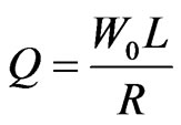 (1)
(1)
The oscillation frequency of oscillator is given by:
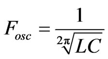 (2)
(2)
where L is the inductance of LC-tank and C is the capacitance.
Phase noise is most important parameter in VCO design therefore; phase noise performance is optimized by using lessons’ formula given by equation (3) [3,5].
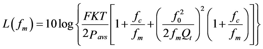 (3)
(3)
where  is the phase noise in dBc/Hz. Qt is the loaded Q of the circuit, fm is the frequency from the carrier, fc is the flicker noise corner frequency, fo is the carrier (oscillator) frequency, T is the temperature in Kelvin, Pavs is the power through the resonator, F is the noise factor of the active device, K is the Boltzmann constant. An important concern in the design of VCOs’ is the variation of the output phase and frequency as a result of noise on the control line. For a given noise in the output frequency is proportional to Kvco because of equation (4) [9].
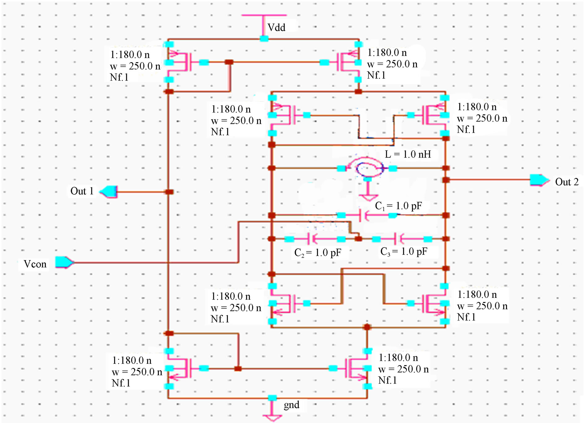
Figure 1. Schematic view of the present VCO design with current mirror.
 (4)
(4)
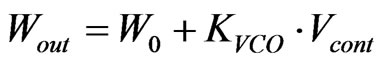
where, W0 is the intercept at Vcont = 0, KVCO is the gain or sensitivity of the circuit, and Wout is output.
Maximum d.c power dissipation = Vsupply × Ibias (5)
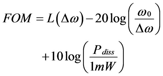
A figure of Merit is a quantity used to characterize the performance of a VCO relative to other VCOs’ of the same type. The power, phase noise, frequency of oscillation, offset from carrier tradeoffs all are taken in the FOM value [3]:
 (6)
(6)
where,  is the oscillation frequency,
  is the offset from the carrier,
  is the phase noise at the specified offset, Pdiss is the DC power consumed by the VCO core. The Simple figure of merit (FOM) to examine various performances can be expressed as [10]:
 (7)
(7)
3. Simulation Results and Discussion
This work is carried out under the environment of cadence software and schematic editor (icfb &) is used for design entry, by using UMC 0.18 µm technology. In this design we have applied 2V as a supply at the center frequency of 3.3 GHz. Simulation have been done and obtained values are: the band width of 1.625 GHz, phase noise of –155.78 dBc/Hz @ 1MHz and –156.89 dBc/Hz @ 100 MHz and phase margin of 180˚ given in table 1. Simulated output voltage responses of this design are presented in figure 2. Phase noise is given in figure 3,

Table 1. Results of VCO design.
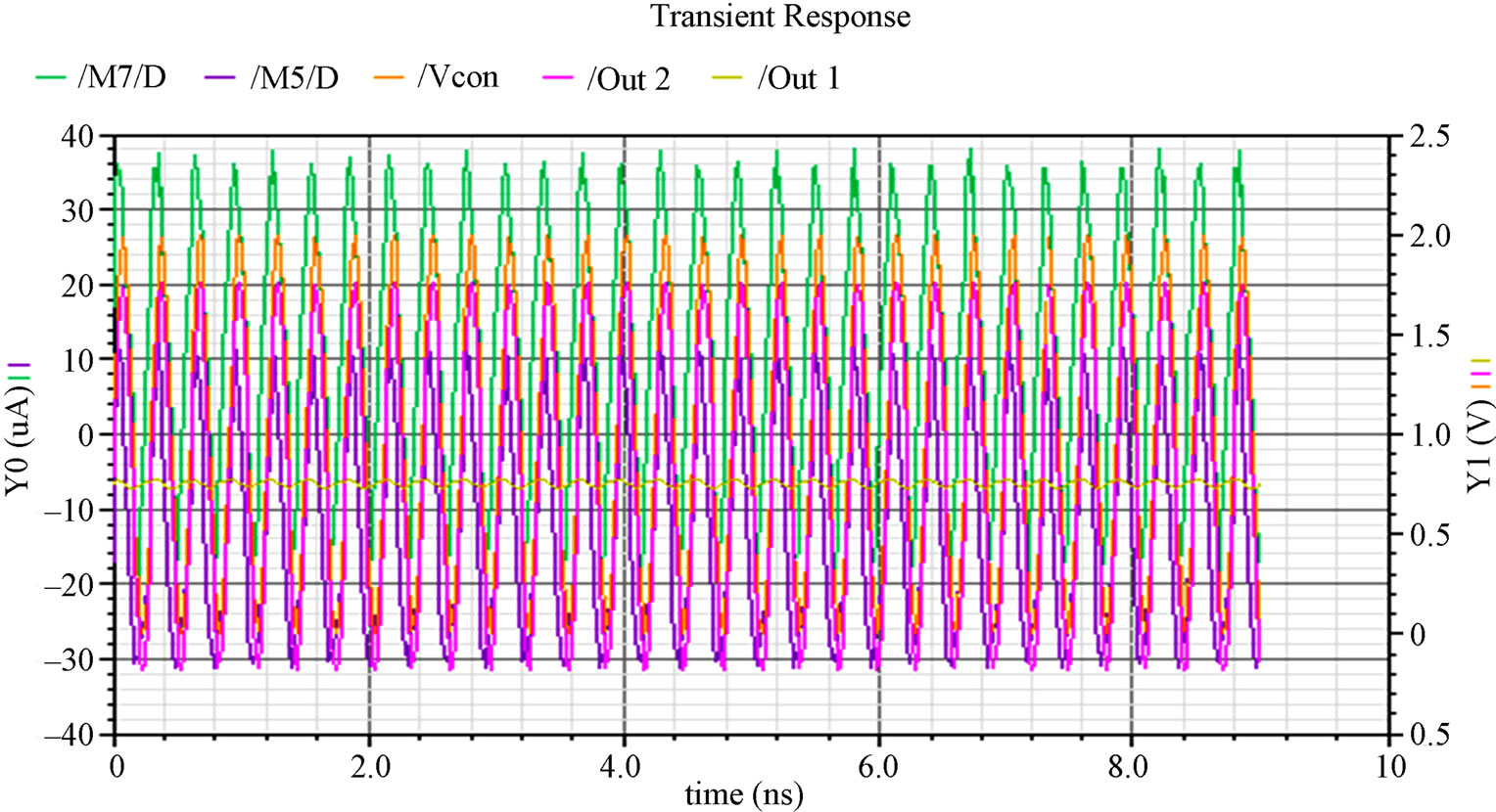
Figure 2. Simulation response of the output voltage.
with the power consumption of 7.40 mW at supply voltage of 2V and FOM is 367 dBF, figure 4 gives the graphical representation of frequency vs voltage. Finally we have designed the layout of the VCO and it is shown in figure 5. Simulation results are verified with earlier published work as given in table 1.
4. Conclusions
This design has improved the performance parameters of the VCO. The realization of a single chip transceiver becomes more demanding, with the need for lower cost, reduced size and less power consumption. The VCO is implemented in cadence environment using 180 nm UMC technology. The design is simulated with different architecture i.e. without current mirror, and with current mirror, improvements are obtained in performance parameters i.e. power consumption is reduced by 2.78% - 5.3%. This paper focused on reasonable phase noise and
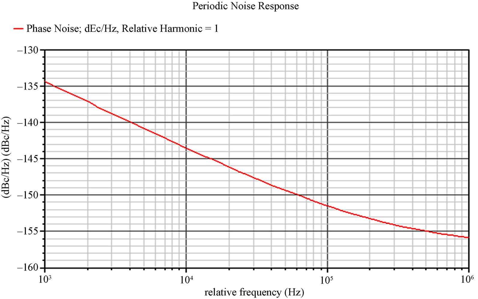
Figure 3. Simulation results of the phase noise @ 1 MHz.
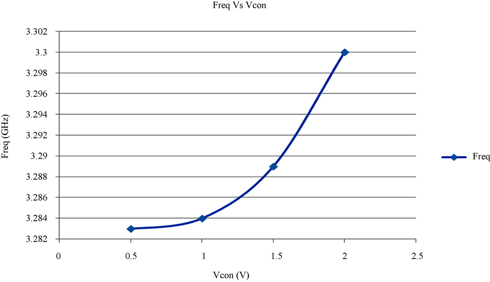
Figure 4. Graphical representation of Freq vs Vcon.
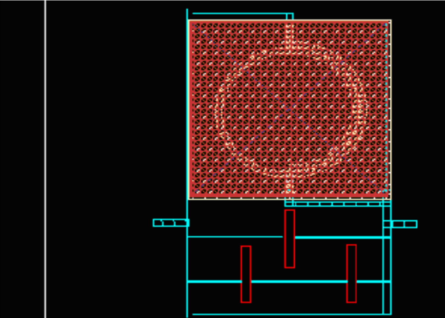
Figure 5. Layout design of VCO using current mirror.
tuning performance at the oscillation frequency of 3.3 GHz. Comparison of works are given in table 1 with earlier published work and improvements are observed.
5. Acknowledgements
This work has been carried out in SMDP VLSI laboratory of the Electronics and Instrumentation Engineering Department of Shri G. S. Institute of Technology and Science, Indore, India. This SMDP VLSI project is funded by Ministry of Information and Communication Technology, Government of India. Authors are thankful to the Ministry for the facilities provided under this project.
REFERENCES
- H. Y. Wang, N. J. Wu and G. L. Shou, “A Novel CMOS Low Phase Noise VCO with Enlarged Tuning Range,” Proceedings of International Conference on Microwave and Millimeter Wave Technology, Nanjing, 21-24 April 2008, pp. 570-573. doi:10.1109/ICMMT.2008.4540456
- W. S. T. Yan and H. C. Luong, “A 900-MHz CMOS Low Phase-Noise Voltage Controlled Ring Oscillator,” IEEE Transactions on Circuits and Systems II: Analog and Digital Signal Processing, Vol. 48, No. 2, 2001, pp. 216-221. doi:10.1109/82.917794
- M. Al-Azab, “Modeling and Characterization of a 5.2 GHz VCO for Wireless Communication,” Proceedings of 26th National Radio Science Conference, Cairo, 17-19 March 2009, pp. 1-7.
- D. B. Leeson, “A Simple Model of Feedback Oscillator Noise Spectrum,” Proceedings of the IEEE, Vol. 54, No. 2, 1966, pp. 329-330. doi:10.1109/PROC.1966.4682
- R. M. Weng and J. Y. Lin, “A 2.4 GHz Low Phase Noise Voltage Controlled Oscillator,” Proceedings of Progress in Electromagnetics Research Symposium, Beijing, 23-27 March 2009, pp. 546-550.
- P. Dudulwar, K. Shah, H. Le and J. Singh, “Design and Analysis of Low Power Low Phase Noise VCO,” Proceedings of the 13th International Conference on Mixed Design of Integrated Circuits and Systems, Gdynia, 22-24 June 2006, pp. 256-259.
- N. Prasad, R. S. Gamad and C. B. Kushwah, “Design of a 2.2 - 4.0 GHz Low Phase Noise and Low Power LC VCO,” International Journal of Computer and Network Security, Vol. 1, No. 3, 2009, pp. 15-18.
- T. H. Lee and A. Hajimiri, “Oscillator Phase Noise: A Tutorial,” IEEE Journal of Solid-State Circuits, Vol. 35, No. 3, 2000, pp. 326-336. doi:10.1109/4.826814
- B. Razavi, “Deign of Analog CMOS Integrated Circuits,” Tata McGraw-Hill, Delhi, 2002.
- T. I. Ahrens and T. H. Lee, “A 1.4-GHz 3-mW CMOS LC Low Phase Noise VCO Using Tapped Bond Wire Inductances,” Proceedings of International Symposium on Low Power Electronics and Design, Monterey, 10-12 August 1998, pp. 16-19.
- P. M. Lu, S. Z. Huang, L. Y. Song and R. Chen, “Design of a 2 GHz Low Phase Noise LC VCO,” Proceedings of International Multi Conference of Engineers and Computer Scientists, Hong Kong, Vol. 2, 18-20 March 2009, pp. 18-21.