World Journal of Condensed Matter Physics
Vol.2 No.2(2012), Article ID:19097,5 pages DOI:10.4236/wjcmp.2012.22017
Theoretical Studies on the Effect of Confinement on Quantum Dots Using the Brus Equation
![]()
Department of Physics, University of Port Harcourt, Port Harcourt, Nigeria.
Email: omictronics@yahoo.com
Received December 7th, 2011; revised January 10th, 2012; accepted January 20th, 2012
Keywords: Quantum dot; Confinment; Nanoparticles; Brus equation
ABSTRACT
Quantum confinement effect in semiconductor quantum dots (QD’s) of CdSe, ZnS and GaAs has been studied using the Brus Equation. It is found that the simple models obtained for the three different semiconductor nanocrystals exhibit the size dependence predicted by the particle-in-a-box model. The result shows that ground state confinement energy is inversely proportional to the size (radius). Thus, as one increases the radius (size), the confinement energy decreases, but never reaches zero. i.e., the lowest possible energy for the quantum dot sample is not zero.
1. Introduction
Quantum dots are semiconductor nanoparticle whose excitons are confined in all three spatial dimensions [1]. It is essentially a tiny zero-dimensional semiconductor crystal with size in the order of nanometers, hence, the name “dot or island”. It is often called artificial atom because of its quantum properties [2] and interactions similar to bulk semiconductor materials. However, their electronic characteristics are closely related to the size and shape of the individual crystal. Generally, the smaller the size of the crystal, the larger the band gap energy; the greater the difference in energy between the highest valence band and the lowest conduction band becomes, therefore, more energy is needed to excite the dot, and the crystal returns to its ground state. In addition to such tuning, the main advantage with quantum dots is the ability to tune the size of the dots for many applications. For instance, larger quantum dots have a greater spectrumshift towards red compared to smaller dots, and exhibit less pronounced quantum properties. Conversely, the smaller particles allow one to take advantage of more subtle quantum effects [3].
Owing to their nano-size, they have very sharp density of states and thus excellent transport and optical properties for detectors [4], lasers [5] and amplifiers [6]. For example, current fiber amplifiers work over a narrow bandwidth. By embedding a gradient multilayer nanofilm (quantum dot of different sizes) in the fiber, the bandwidth would be increased in several folds.
Quantum dots also have large quantum yield. i.e. the percentage of absorbed photons that result in emitted photons, what is being studied for potential use in more effective solar cell [7].
In the bulk semiconductor material (several times bigger than 10 nm), charge carriers can have a range of energies. These energies are so close together that they can be described as continuous (see figure 1). There is a certain forbidden range of energies called band gap. Almost all carriers naturally occupy the energy levels below the band gap (valence band) and only very few of them are in the conduction band (above the band gap). They can jump to the conduction band when they get additional energy from outside (heat, radiation, etc.) and they leave a hole in the valence band. This electron-hole pair is called an exciton which is the true nature of a charged dot and has a lot of properties similar to the hydrogen atom [8].
From figure 1 we can see that ΔEnano is greater than ΔEbulk; this is due to the reduction in dimensions of the QD which increases the confinement energy in the dot (nanoparticle).
Confinement in quantum dots can also arise from electrostatic potentials generated by external electrodes, doping, strain or impurities [9].
The width of the quantum dot band gap depends on its size and chemical composition, making it easy to tune absorption and emission spectra, what is impossible for atoms, but desirable for optical properties [3].
In this research, we try to look at how the Brus equation can be used to obtain the confinement energy at various dots radii in other to deduce the confinement nature associated with the individual dot understudy.
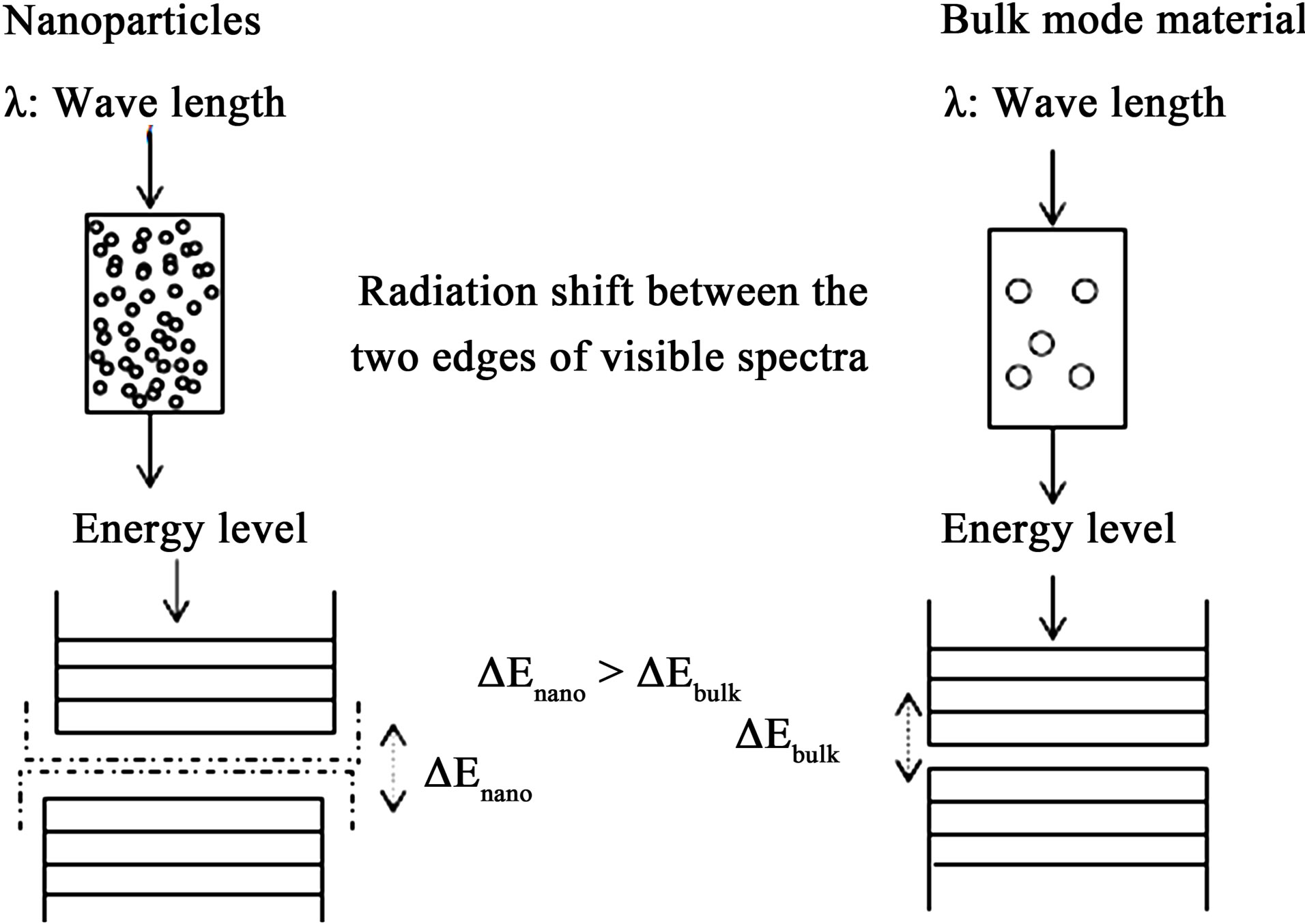
Figure 1. Quantum confinement is responsible for the increase of energy difference between energy states and bandgap [8].
2. The Brus Equation
Brus gave the first theoretical calculation for semiconductor nanoparticles (using CdS and CdSe as examples) based on “effective mass approximation” (EMA). In this approximation, an exciton is considered to be confined to a spherical volume of the crystallite and the mass of electron and hole is replaced with effective masses (me and mh) to define the wave function [10].
 (1)
(1)
where,
 = band gap energy of quantum dot;
Ebulk = band gap energy of bulk semiconductor;
R = radius of quantum dot;
 = effective mass of excited electron;
 = effective mass of excited hole;
h = Planck’s constant.
Kayanuma accounted for the electron-hole spatial correlation effect [11] and modified the Brus Equation. Based on the modified equation, the size dependence on the band gap energy of quantum dots can be quantified as follows:
 (2)
(2)
whereh = Planck constant
 = effective mass of excited electron
 = effective mass of excited hole R = radius of quantum dot e = electronic charge
 = permittivity of vacuum
 = relative permittivity
 = Rydberg energy The first term in the right hand side of equation (2) represents the band gap energy of bulk materials, which is characteristic of the material. The second additive term of the equation represents the additional energy due to quantum confinement having a
  dependence on the band gap energy. It can indeed be thought of as the infinite square-well contribution to the band gap. The third subtractive term stands for the columbic interaction energy exciton having
  dependence (often neglected due to high dielectric constant of semiconductor material). The numerical factor in this term originates from calculations of wave function overlap integrals and its value may vary slightly from material to material. The last subtractive term, stands for spatial correlation effect (independent of radius) and significant only in case of semiconductor materials with low dielectric constant.
However equation (2) is only approximated and is expected to fail. In assuming the effective mass approximation he noted that due to the significant number of the electronic wave functions inside the nanocrystal which have wave function overlapping with the edge of the crystal (where the potential landscape is no longer periodic). As a result, equation (2) is expected to fail for very small nanocrystals [12].
If we assume that the nanocrystal is Spherical. Decoupling of the Schrodinger equation into a radial part (depending on r) and a spherical harmonic part (depending on the angles  and
and  ) is possible. This significantly reduces the difficulty of calculating the energy states because the wave functions involved are now products of the two separate wave functions functions:
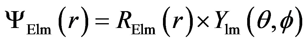
This approximation is often quite good since most chemically synthesized nanocrystals have aspect ratios (defined as the ratio between the longest and shortest axes) smaller than 1. High aspect ratio nanocrystals can also be synthesized [13] and for such nanocrystals this approximation indeed breaks down.
In the Infinite potential barrier, the true potential-step at the surface of a nanocrystal is not infinite. A typical value for this barrier is in the order of 1 to 3 eV (due to the work function of the semiconductor). This value is quite large compared to typical electron and hole energies. As a result, only a small fraction of the electron and hole wave functions will “leak” out of the nanocrystal. This can result in tunnel conductivity from the nanocrystal to its surroundings (i.e. other nanocrystals or a conducting substrate) and an overestimation of the semiconductor band gap based on equation (2). The exact nature, form and magnitude of the surface potential will only become important in very small nanocrystals or for nanocrystals with an exceptionally low work function. This infinite potential barrier approximation also implies that Eg(R) is insensitive to an externally applied potential and to the surroundings of the nanocrystal. The effect of the surroundings will indeed probably be very small, but the effect of an externally applied potential can be quite significant. Therefore, this approximation is expected to fail when the externally applied potential becomes too large.
The Brus Equation can be used to describe the emission energy of quantum dot semiconductor nanocrystal in terms of the band gap energy (Eg), planck’s constant (h), the radius of the quantum dot (r), the mass of the excited electron ( ), and the mass of the electron hole (
 ) [13]. The radius of the quantum dot affects the wavelength of the emitted light due to quantum confinement, and this describes the effect of changing radius of the quantum dot on the wavelength emitted (
 where c = speed of light in m/s).
The overall Brus Equation for calculating the emission energy is given as:
 (3)
(3)
where
ΔE = the emission energy.
3. Results
We presents the values of the parameters used and the results obtained with the dimensionless and physical quantities used in this research, the ground state confinement energy, emission energy as well as wavelength as a function of radius for three different semiconductor quantum dots that were calculated. In arriving at the results, several parameters were used, for Cadmium Selenide, Zinc Sulphid and Gallium arsenide as in table 1 below.
Table 1 showing material parameter used for the computation of the confinement energies at various radii which is less than the bohr radius aB [8].
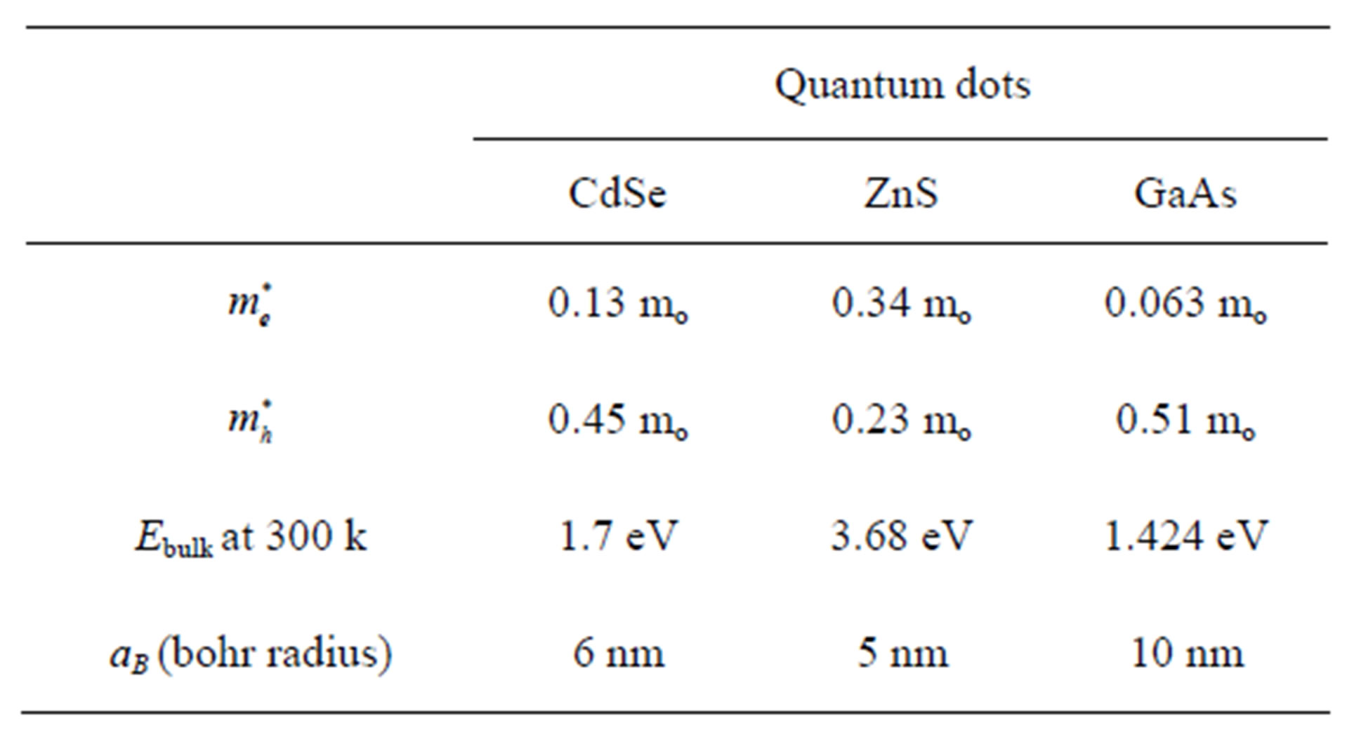
Table 1. Table type styles (table caption is indispensable).
Table 1 showing material parameter used for the computation of the confinement energies with the dot radii of 0.9, 1.2, 1.44, 1.92, 2.40, 2.96, 3.5, 4.2 and 4.8 for CdSe, 0.75, 1.25, 1.75, 2.25, 2.75, 3.25, 3.75, 4.0 and 4.5 for ZnS, 1.5, 2.0, 2.5, 4.0, 5.5 6.6, 7.0, 7.5 and 8.0 nm for GaAs, that was assumed for the computation.
The ground state confinement energies (ECF), the emission energies and wave length at various dot radii were computed using equation (3). Also the columbic term is ignored in the equation.
4. Discussion of Results
The graphs of ground state confinement energy against size (radius) for cadmium selenide (CdSe), gallium arsenide (GaAs), and zinc sulphide (ZnS) semiconductor quantum dots in Figures 2-4 respectively show the dependence of confinement on the size of quantum dots. The result shows that ground state confinement energy is inversely proportional to the size (radius). The graphs are asymptotic to the radius (horizontal) axis. Thus, as one increases the radius (size), the confinement energy decreases, but never reaches zero. i.e., the lowest possible energy for the quantum dot sample is not zero.
The confinement energy is observed in quantum dots through an increase in the energy of the band gap. Confinement begins when radius of the quantum dot sample is comparable or of the order of the exciton bohr radius,
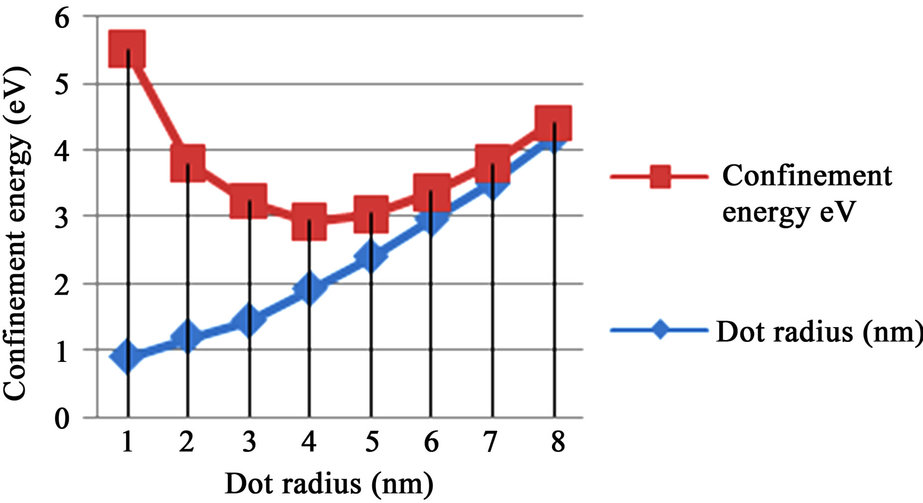
Figure 2. Showing the ground state confinement energy and radius for CdSe.
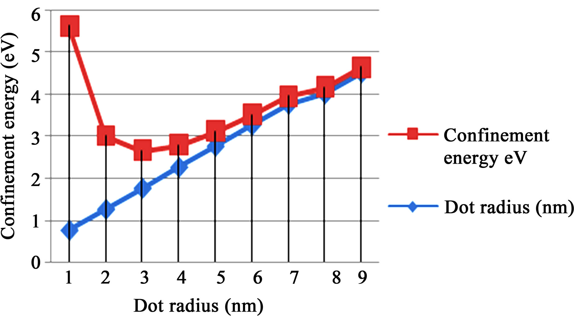
Figure 3. Showing the ground state confinement energy and radius for ZnS.
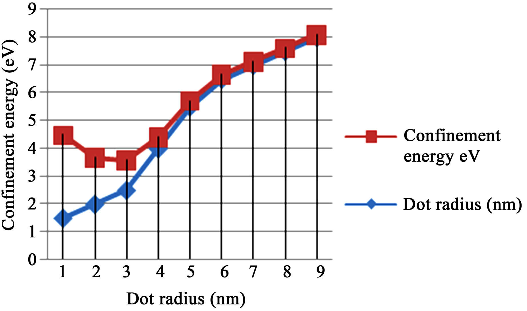
Figure 4. Showing the ground state confinement energy and radius for GaAs.
aB (6 nm for cadmium selenide, 10 nm for gallium arsenide, and 5 nm for zinc sulphide). In order words when the size is comparable to 2 aB (doubles the exciton bohr radius). The confinement energy increases as the size of the quantum dot is gradually reduced until the cluster and magic number limit for the particular crystal is reached. At this limit, Brus Equation no longer holds, and the crystal losses its stability [14]. The energy spectrum is discrete rather than continuous in the confinement regime. Thus, only certain energies are allowed for a quantum dot of a given size. The density of states gets peaked at these energies. Experimentally, this can be observed in the absorption spectrum of the given quantum dot [6].
The confinement region is subdivided into strong confinement regime and weak confinement regime [15]. It must however be noted that in the weak confinement regime, the energy levels form a near continuum. In Figure 2, sharp increase in confinement energy begins at r = 1.92 nm. Thus, the limit of strong confinement for cadmium selenide is at size 3.84 nm, which corresponds to confinement energy of about 1.015 eV. Beyond this limit, the discrete nature of the energy spectrum becomes more apparent until one gets to the cluster and magic number limit. Figure 3 shows that a sharp increase in confinement energy for gallium arsenide begins from size 4 nm up to the cluster and magic number limit. Thus, the limit or threshold for strong confinement corresponds to energy of about 0.421 eV. Similarly, in figure 4, the strong confinement limit for zinc sulphide quantum dot is observed when the size is scaled down to about 4.50 nm radius of 2.25 nm. This corresponds to confinement energy of about 0.543 eV.
5. Conclusions
The confinement energy can be seen as a consequence of the particle-in-a-box model. The simple models obtained for the three different semiconductor nanocrystals exhibit the size dependence predicted by the particle-in-a-box model. The experimental observation of the size dependence on the band gap energy is in good agreement with the theoretical models for the semiconductor nanocrystals considered. The confinement of electrons in semiconductor quantum dots increases dramatically with decrease in its size (radius). The larger the exciton Bohr radius, the wider the range of tunability. Also the continuum observed in the conduction band and valence band in the case of bulk materials is replaced with discrete atomic like energy levels as the particle size decreases.
The degree of confinement among the three nanocrystals considered is found to be strongest in cadmium selenide, followed by zinc sulphide and then gallium arsenide from this one can say that there will be more strain energy in CdSe.
However, it is extremely difficult for one to actually predict the size, shape, composition, and surface density of quantum dot given growth parameters and material parameters. Hence more Intensive Research/investigation should be carried out to develop a single model that can predict the size, shape, composition, and surface density of quantum dots.
REFERENCES
- M. A. Reed, E. S. Hornbeck, M. R. Deshpande, R. G. Wheeler, R. C. Bowen, J. N. Randal and W. R. Frensley, “Quantum Dots,” Scientific American, Vol. 268, No. 1, 1993, pp. 118-123. doi:10.1038/scientificamerican0193-118
- R. D Schaller and V. I. Klimov, “High Efficiency Carrier Multiplication in PbSe Nanocrystals: Implications for Solar Energy Conversion,” Physical Review Letters, Vol. 92, No. 18, 2004, Article ID 186601. doi:10.1103/PhysRevLett.92.186601
- C. Wang, M. Shim and P. Guyot-Sionnest, “Electrochromic Nanocrystal Quantum Dots,” Science, Vol. 291, No. 5512, 2001, pp. 2390-2392. doi:10.1126/science.291.5512.2390
- P. Martyniuk and A. Rogalski, “Quantum-Dot Infrared Photodetectors: Status and Outlook,” Progress in Quantum Electronics, Vol. 32, No. 3-4, 2008, pp. 89-120. doi:10.1016/j.pquantelec.2008.07.001
- A. A. Lagatsky, C. G. Leburn, C. T. A. Brown, W. Sibbett, S. A. Zolotovskaya and E. U. Rafailov, “Ultrashort-Pulse Lasers Passively Mode Locked by Quantum-Dot-Based Saturable Absorbers,” Progress in Quantum Electronics, Vol. 34, No. 1, 2010, pp. 1-45. doi:10.1016/j.pquantelec.2009.11.001
- J. Harbold and M. Plisch, “The Quantum Dot,” Cornell University, New York, 2008. http://www.cns.cornell.edu/documents/QuantumDots.pdf
- O. Yoshitaka, “Solar Quest,” Nature Photonics Technology Conference, Tokyo, 19-21 October 2010.
- J. Sinclair and Dr. Dagotto, “An Introduction to Quantum Dots: Confinement, Synthesis, Artificial Atoms and Applications,” Solid State II Lecture Notes, University of Tennessee, Knoxville, 2009.
- P. Michler, “Single Quantum Dots: Fundamentals, Applications and New Concept, Physics and Astronomy Classification Scheme (PACS),” Springer-Verlag, Berlin, 2003.
- L. E. Brus, “Electron-Electron and Electron-Hole Interactions in Small Semiconductor Crystallites: The Size Dependence of the Lowest Excited Electronic State,” Journal of Chemical Physics, Vol. 80, No. 9, 1984, p. 4403. doi:10.1063/1.447218
- Y. Kayanuma, “Quantum-Size Effects of Interacting Electrons and Holes in Semiconductor Microcrystals with Spherical Shape,” Physical Review B, Vol. 38, No. 14, 1988, pp. 9797-9805. doi:10.1103/PhysRevB.38.9797
- J. Pan, A. Bahel, V. Mushti and M. V. Ramakrishna, “Chemistry of Nanoscale Semiconductor Clusters,” Chemical Physics, 1994, in press. http://arxiv.org/pdf/chem-ph/9506002v1.pdf
- T. Kippeny, L. A. Swafford and S. A. Rosnethal, “Semiconductor Nanocrystals: A Powerful Visual Aid for Introducing the Particle in a Box,” Journal of Chemical Education, Vol. 79, No. 9, 2002, pp. 1094-1100. doi:10.1021/ed079p1094
- L. E Brus, “A Simple Model for the Ionization Potential, Electron Affinity and Aqueous Redox Potentials of Small Semiconductor Crystallites,” Journal of Chemical Physics, Vol. 79, No. 11, 1983, pp. 5566-5571. doi:10.1063/1.445676
- J. M. Harbold, “The Electronic and Optical Properties of Colloidal Lead Selenide Semiconductor Nanocrysta,” Ph.D. Dissertation, Cornell University, New York, 2005.