Journal of Sensor Technology
Vol.2 No.3(2012), Article ID:22875,9 pages DOI:10.4236/jst.2012.23022
Online Capacitance Modeling Tool for Conductors Represented as Simply-Connected Polygonal Geometries in 2D
1School of Mechanical Engineering and Birck Nanotechnology Center, Purdue University, West Lafayette, USA
2School of Electrical and Computer Engineering, Purdue University, West Lafayette, USA
Email: *li200@purdue.edu
Received May 1, 2012; revised June 4, 2012; accepted July 5, 2012
Keywords: Capacitance; Conformal Mapping; Online Modeling and Simulation Tool; Schwarz-Christoffel Mapping
ABSTRACT
We present an online tool for calculating the capacitance between two conductors represented as simply-connected polygonal geometries in 2D with Dirichlet boundaries and homogeneous dielectric. Our tool can be used to model the so-called 2.5D geometries, where the 3rd dimension can be extruded out of plane. Micro-electro-mechanical systems (MEMS) with significant facing surfaces may be approximated with 2.5D geometry. Our tool compares favorably in accuracy and speed to the finite element method (FEM). We achieve modeling accuracy by treating the corners exactly with a Schwarz-Christoffel mapping. And we achieve fast results by not needing to discretize boundaries and subdomains. As a test case, we model a MEMS torsional actuator. Our tool computes capacitance about 1000 times faster than FEM with 4.7% relative error.
1. Introduction
MEMS technology has been rapidly developed and expanded in the past 30 years in various industries such as automobile, consumer electronic, health, and telecommunication. In 2011, MEMS market reached $12B [1], with MEMS capacitive sensors comprising significant portion of the market. For example, capacitive MEMS are the enabling technology in automobile airbags, accelerometers for cell phones and video game controllers, affordable inertial navigation, etc. Capacitive sensors offer lower noise performance and lower power consumption. They are easy to fabricate, do not require uncommon materials, and do not consume DC power [2].
Quick and accurate capacitance modeling and simulation of deformable structures can be beneficial for the following reasons. Faster simulation results enable faster transient analyses or faster parameterized design space explorations. More accurate modeling enables more accurate determination of surface forces due to fringing fields, of dielectric breakdown due to high charge density, gap pull-in instability, comb asymmetry instability, of charge storage for dynamic capacitive circuit element analysis, of capacitance signal to noise ratio, coarse surface profiles, and of parasitic capacitance analysis.
Some popular methods used for computing the capacitance in MEMS include parallel-plate approximation, conformal mapping, and distributed element methods. Distributed element methods include integral equation solvers and differential equation solvers. Examples of integral equation solvers include the method of moments or the boundary element method (BEM), and the fast multipole method (FMM). An example of differential equation solvers is the FEM.
Parallel-plate approximation [3] applies to configurations where there is significant electrode overlap within close proximity as to approximate a portion of a parallel plate. Because the expression for the parallel plate approximation is analytical, computation is fast. However, the capacitance determined by the parallel plate approximation is usually lower than the actual capacitance because the method ignores high charge density at corners and parasitic capacitance.
Distributed element methods are often used when the MEMS geometry cannot be represented as a portion of a parallel plate. In BEM, surfaces boundaries are discretized into elements. BEM is the general method of choice when the dielectric is homogeneous [4]. BEM tools such as FastCAP [5] and CENEMS [6] find the surface charge density in 3D and 2.5D, respectively, given surface voltages. The notion of 2.5D applies to symmetric 2D geometries that can be rotated 360 degrees to represent 3D, or 2D geometries that can be extruded orthogonally out of plane into an approximate 3D configuration. Prescribing a voltage on a geometric surface is a Dirichlet boundary condition. The capacitance is found by integrating the surface charge density and dividing by the voltage difference. For inhomogeneous dielectric layers, BEM can be used while the homogeneous dielectric Green’s function is replaced by layered dielectric medium Green’s function. In FEM, the boundaries and subdomains are discretized into elements. FEM is useful for modeling inhomogeneous dielectrics or analyzing the potential field or the electric field. FEM is used in commercial tools such as COMSOL™, CoventorWare™, and IntelliSuite™. In general, distributed element methods require convergence analysis, where the results of successive simulations with mesh refinement of the same scale are compared until a desired tolerance level is achieved. Distributed element methods are usually computationally intensive, requiring a significant amount of computer memory and time.
Conformal mapping methods are useful in MEMS when the configuration can be approximated as 2.5D by either rotating about an axis or extruding orthogonally out of plane. Conformal mapping is based on a branch of mathematics called complex analysis, which conformally maps the field and boundary of simply-connected geometries from one configuration to another. When conformal mapping is used for modeling capacitance, it is usually done by mapping an arbitrary geometry configuration that is difficult to solve to a configuration that is easy to solve. In particular, such arbitrary geometries are transformed to truly infinite parallel plate configuration, which is accurate, unlike the partial parallel-plate approximation mentioned above. Although such geometric transformations can be quite extreme, the capacitance is invariant during one or more conformal mappings [7]. If the conformal mapping is done through the upper-half complex plane, then it is called Schwarz-Christoffel mapping (SCM).
Examples of SCM used in MEMS are as follows. To reduce computational cost, Sumant et al. used SCM to avoid re-meshing after RF MEMS deformation in an electrostatic structure [4]. To develop an analytical model of a repulsive electrostatic actuator, He and Mrad divided an electrostatic domain into four subdomains to find an analytical SCM expression, which transformed the subdomains into a strip plane to model capacitance [8]. To develop 3D SCM models for interdigitated comb fingers, Johnson and Warne limited their model to finger thicknesses that are much smaller than the engagement distance and finger gap [9]; Yeh et al. ignored the electrostatic contribution of the ground plane [10]; and Bruschi et al. 2004 created eight subdomains in 2.5D to find a SCM solution [7].
Such SCM methods are for specific geometries only. There does not appear to be a preexisting SCM tool for computing the capacitance for more arbitrary MEMS geometries. We proved that SCM can be used for determining the capacitance of arbitrary simply-connected 2D geometries in [11]. In this paper, we extend those results into an online tool that can be used to investigate the capacitance, charge, and force of a variety of MEMS geometries in 2D. The numerical solver in our tool is the SCM MATLAB™ toolbox developed by [12].
Compared to distributed methods in 2D, solution times by SCM is generally faster by avoiding the large number of coupled equations associated with distributed methods. Instead of using a large number of elements to estimate geometric corners, SCM treats corners exactly. And if there is a small number of vertices in the configuration, then SCM can become analytical. However, SCM method only accommodates for homogeneous dielectric mediums.
The preliminary results of the project have been published in [13], and the completed results with thorough analyses are presented here. The rest of the paper is organized as follows. In Section 2 we overview particular aspects of SCM theory. We add the theoretical derivations of energy, charge, and electrostatic force which is not presented in [13]. In Section 3 we present the current graphical user interface (GUI) of our online capacitance modeling tool which is not presented in [13]. In Section 4 we investigate a MEMS torsional actuator as a test case of SCM and compare our results to FEM and analytical approximation. We add convergence analysis in SCM and compare the results found by three different methods which are not presented in [13]. And in Section 5 we summarize our findings.
2. Theory
In this section we overview the process of mapping a region from a physical plane (Z-plane) into a strip plane (F-plane). A strip plane consists of infinitely parallel boundaries, which is ideal for determining capacitance using the infinite parallel-plate model. We also discuss how capacitance, charge, and force can be determined.
2.1. Mapping from a Physical Plane to a Parallel Strip
We illustrate the mapping process from the physical Z-plane to the strip F-plane. The basic Schwarz-Christoffel formula is a conformal mapping from the upper half of the complex W-plane (the canonical domain) to the interior of a simply-connected polygon in the Z-plane (the physiccal domain) as shown in Figure 1. By simplyconnected polygon, we mean the polygon having no in-
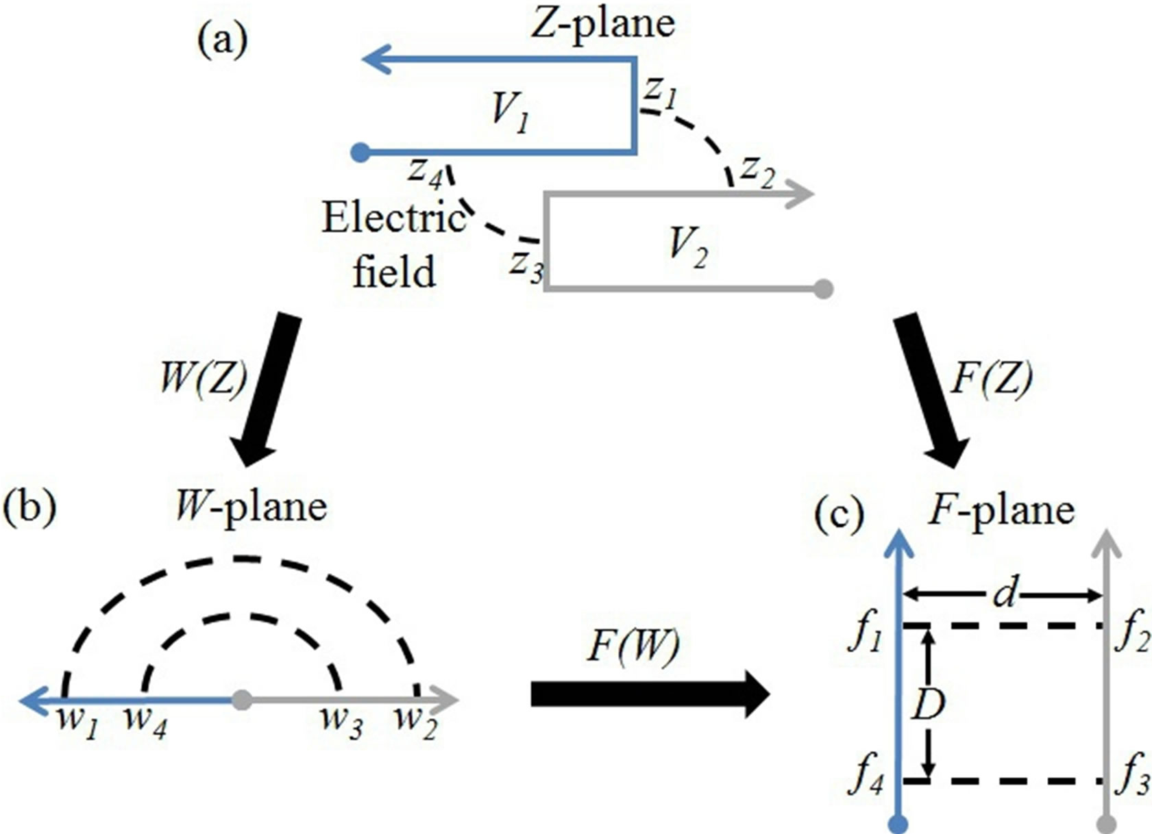
Figure 1. Schematic of the mappings from the physical Z-plane to the strip F-plane. (a) We show a 2D geometry configuration with two electrodes having Dirichlet boundary conditions, potential V1 and V2. We model the capacitance within the region bounded by two electrodes and two electric field lines. The vertices of the electrodes with the arrows and the dots meet at infinity; (b) We show the mapping, W(Z), from the physical Z-plane onto the upper half of the complex W-plane. The region of interest in (a) is mapped as a region with a semi-circular shape; (c) We show the mapping F(W) from the upper half of the complex W-plane onto a strip F-plane. The distance between two electrodes is d, and the distance between two electric field lines is D. We choose the strip plane because it represents the cross section of a true infinite parallel plate. The capacitance of any region of the F-plane can be calculated exactly. Our tool finds the locations of the electric field lines in the strip plane based on the locations in the physical plane, denoted as mapping F(Z).
tersecting sides [14]. The pre-image of the vertices, zi in the Z-plane, or prevertices, are real and denoted by wi in the W-plane. Except in special cases, the prevertces, zi, cannot be com-puted analytically. This is known as the Schwartz-Christoffel parameter problem which is solved by using the SCM MATLAB toolbox numerically [12]. The toolbox provides the numerical relationship between the vertices in the Z-plane and the prevertices in the Wplane, denoted as W(Z) in Figure 1. Another conformal mapping F(W) maps the W-plane onto the strip F-plane so that the simply-connected polygon in the Z-plane is mapped into a rectangular in the F-plane.
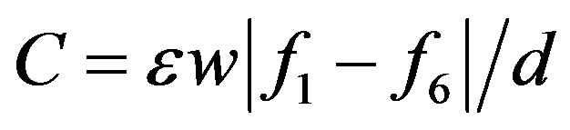
In Figure 1(a), we show a 2D geometric configuration with two electrodes having Dirichlet boundary conditions, potentials V1 and V2, in the physical Z-plane. The 3rd dimension is extruded out of the plane. Figure 1 depicts the capacitance within the region bounded by two electrodes and two electric field lines. The vertices of the electrodes with the arrows and the dots meet at infinity. The region shown in Figure 1(a) is mapped onto Wplane shown as semi-circular electric field lines. This semicircular field is then mapped onto the F-plane as infinitely parallel equipotentials with distance d between two bounding electrodes and distance D between the two electric field lines from the physical Z-plane. We choose the strip plane because it represents a true infinite parallel-plate, the capacitance of the region with the rectangular shape can be calculated exactly as
 (1)
(1)
where ε is the permittivity of the dielectric between two electrodes, and w is the out-of-plane width. Since the capacitance is invariant during one or more conformal mappings, we can calculate exactly in the strip F-plane for any rectangular region bounded between the two electrodes and two electric filed lines. The result is the capacitance between the corresponding electric field lines and electrode geometries in the physical Z-plane.
2.2. Energy, Capacitance, Charge, and Force
The electrostatic energy U stored in a capacitor and the total charge Q can be expressed as
 (2)
(2)
and
 (3)
(3)
The electrostatic force Fd along the direction d is given by the negative gradient of the stored energy [1] as
 , (4)
, (4)
where U is the electrostatic energy stored in the capacitor given in (2). Substituting (2) into (4) we have
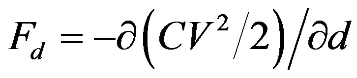 . (5)
. (5)
Since the potential difference V does not change, we have
 (6)
(6)
The derivative 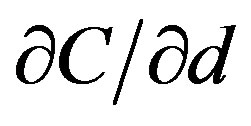 can be approximated by a finite difference for a small displacement
  of the electrodes as
 . (7)
. (7)
3. GUI of Our Online Capacitance Modeling Tool
Our capacitance modeling tool is installed at nanoHUB. org. Users may configure and run simulations over the web with remote computation. Simulations remotely run over the clusters located at Purdue University so that the computational memory requirement for users’ local computers is minimal.
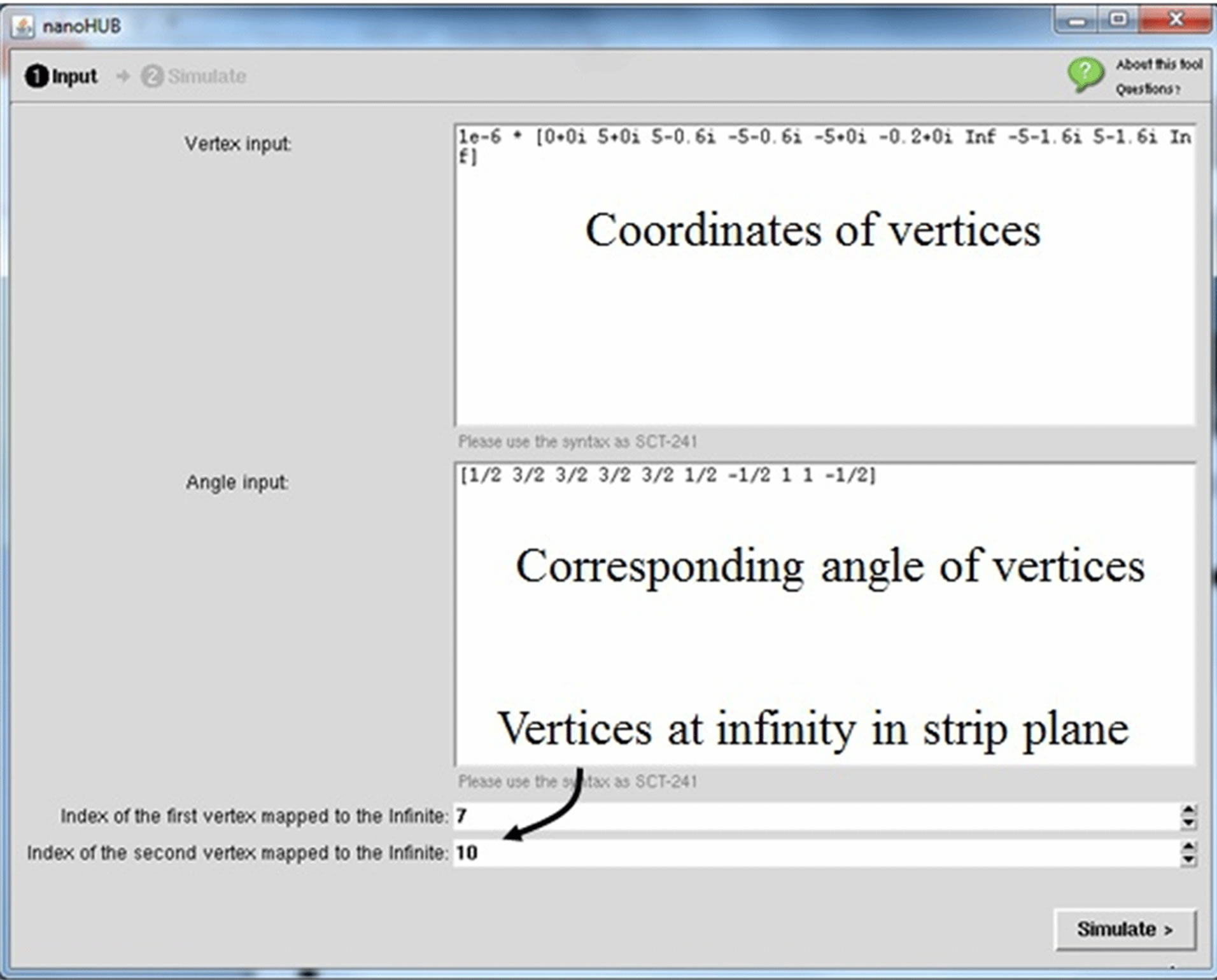
In Figure 2, we present the GUI of our online capacitance modeling tool (version 0.1). In this version, we only provide the capacitance result, while the calculations of the charge and electrostatic force will be developed in the future versions. In Figure 2(a), we show the
 (a)
(a) (b)
(b)
Figure 2. Online GUI of our capacitance modeling tool. (a) GUI for configuring the geometry. The coordinates and the angles of the vertices of the geometry are defined by the user. The user also defines two vertices that are to be mapped to infinity in the strip F-plane. The simulation runs on nanoHUB clusters remotely; (b) GUI of the output. The device configuration is shown together with the electric and equipotential field lines. The calculation of capacitance for 2D is provided by selecting the Capaticance option in the pull-down menu.
GUI of the input phase. The coordinates and the angles of the vertices are defined by the users for the device configuration to be simulated. And users need to define two vertices that to be mapped to the infinite in the strip F-plane. The simulation will start to run remotely on the nanoHUB clusters once the Simulate button is clicked. Our tool uses the SCM MATLAB toolbox [12] to determine the locations of those vertices in the strip F-plane and calculate the capacitance by using (1). In Figure 2(b), we show the GUI of the output phase. The device configuration is shown based on the vertices and angles input along with the electric field and equipotential lines. The capacitance per unit depth result (not shown in figure) for the 2D configuration is provided numerically by selecting the Capaticance per Unit Depth option in the pull-down menu.
4. Test Case: Torsional Actuator
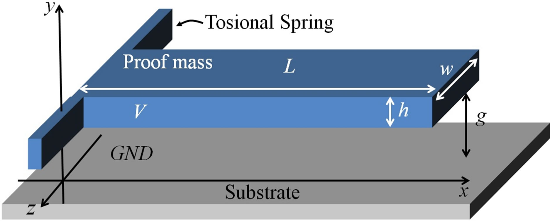
Electrostatic torsional actuators have been widely used. The torsional actuator has claimed about 50% of the market share in projector sales, and its performance is orders faster than competing LCD technology [15]. Several types of torsional actuators are shown in Figure 3. In this section, we model the capacitance of a MEMS torsional actuator at different states of angular deflection.
For our test case, we consider the configuration shown in Figure 4. It consists of a conductive plate supported by a torsional flexure above a conductive substrate. Upon electrostatic actuation, the plate is attracted to the substrate and rotates about its far left end (Figure 4(b)). The plate has length L, out-of-plane width w, cross sectional thickness h, and the initial gap between the plate and substrate is g. The potential difference between the plate and substrate is voltage V. Although in-plane (xy-plane) fringing field is considered, we have assumed that the out-of-plane (yz-plane) dimension is large enough, or that the gap is small enough, so that the out-of-plane fringing fields are not significant. Otherwise, we would consider modeling the cross section of the plate about the yz-plane as well. Below we compare three models. In Subsection
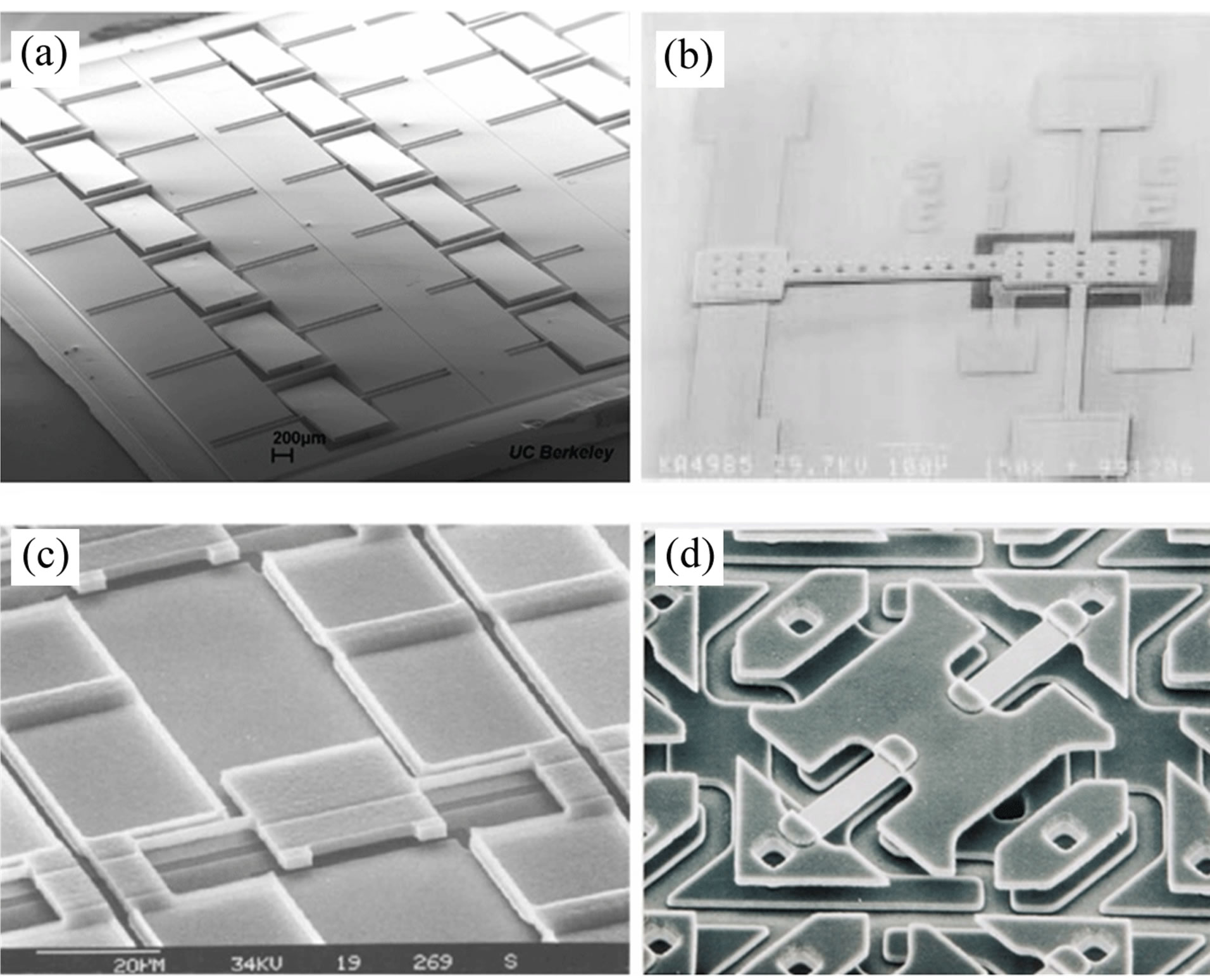
Figure 3. SEM images of four torsional actuators. (a) Torsional actuators using self-aligned plastic deformation of silicon potentially used for MEMS scanning mirrors applications [16]; (b) A low-voltage actuated micromachined microwave switch used for mobile RF telecommunication systems [17]; (c) A torsional micromirror used for light modulator arrays [18]; (d) A torsional micro-mirror by Texas Instruments commercially used in digital light projection (DLP) systems.
 (a)
(a)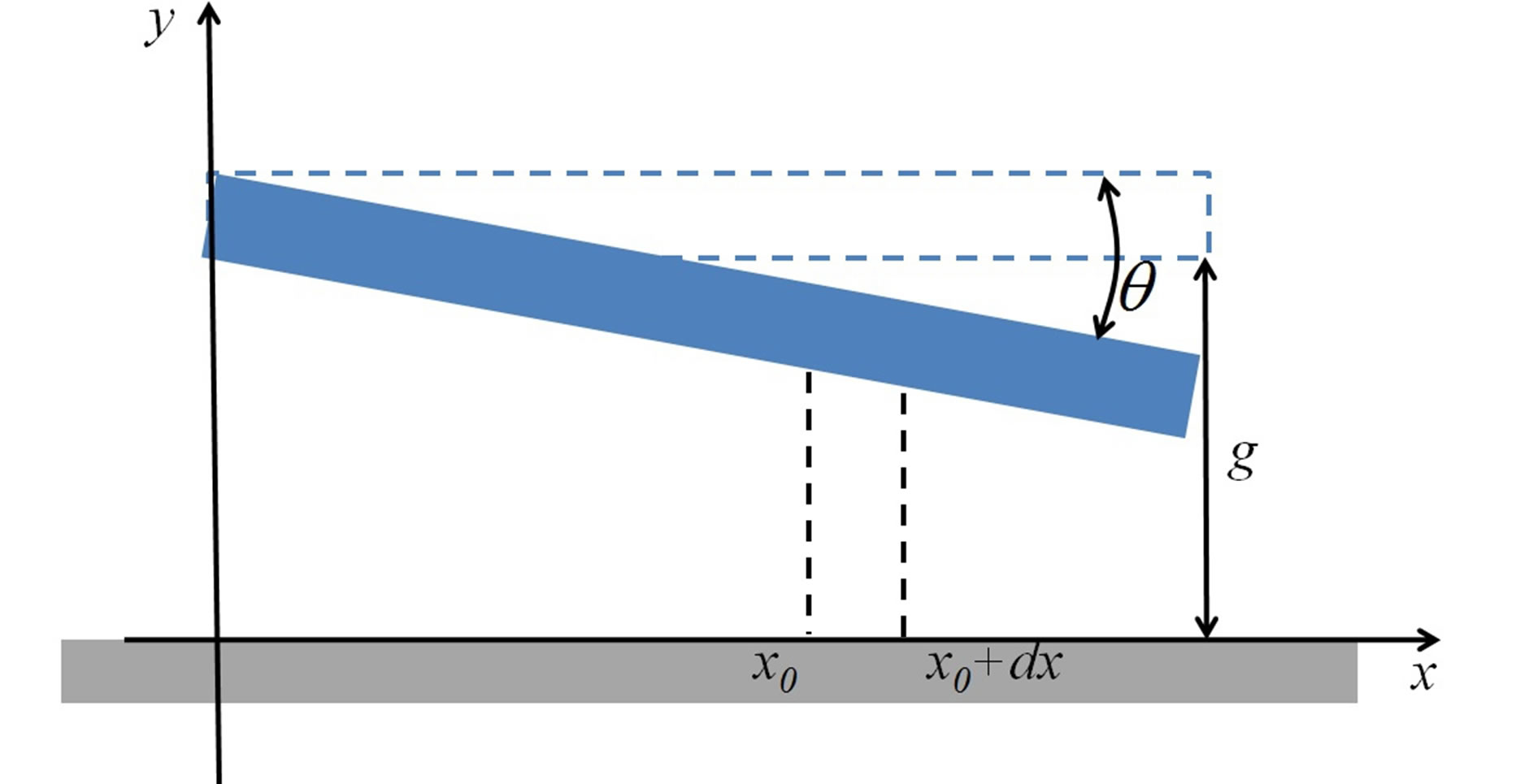 (b)
(b)
Figure 4. MEMS torsional actuator configuration. A 3D view of a MEMS torsional actuator is shown in (a). The length, out-of-plane width, and cross sectional thickness of the plate are L, w, and h. The initial gap between the plate and the electrode is g. We model this device by considering the 2D cross section shown in (b), which can be extruded by amount w out-of-plane for 2.5D. The plate rotates an angle θ.
4.1 we derive an analytical capacitance model based on the parallel-plate approximation. In Subsection 4.2 we use our online tool to model the capacitance of the actuator. In Subsection 4.3 we model the capacitance of the actuator using in a FEM tool. And in Subsection 4.4 we compare these results.
4.1. Parallel-Plate Approximation Model
We model the angled configuration in Figure 4(b) using a parallel-plate approximation by discretizing the facing surfaces of the plate and substrate into columnar portions of a parallel plate. One such columnar portion is depicted in Figure 4(b) bounded by the two vertical dashed lines at positions x0 and x0 + dx, the horizontal substrate surface, and the angled plate surface. Similar to Cheng et al., we approximate angled plate surface is as being horizontal by considering a small dx amount of it [3]. The parallel-plate capacitance  of such a small portion can be approximated as
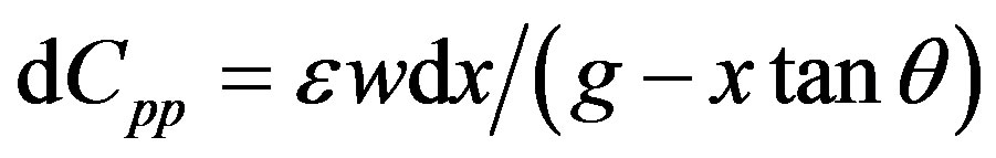 . (8)
. (8)
By integrating (8) along the length of the plate, the net capacitance is
 (9)
(9)
The fringing field effect and surface charge contributions from the sides and upper surfaces are not modeled with (9). The capacitance in (9) as a function of angle is discussed in Subsection 4.4 and plotted in Figure 5.
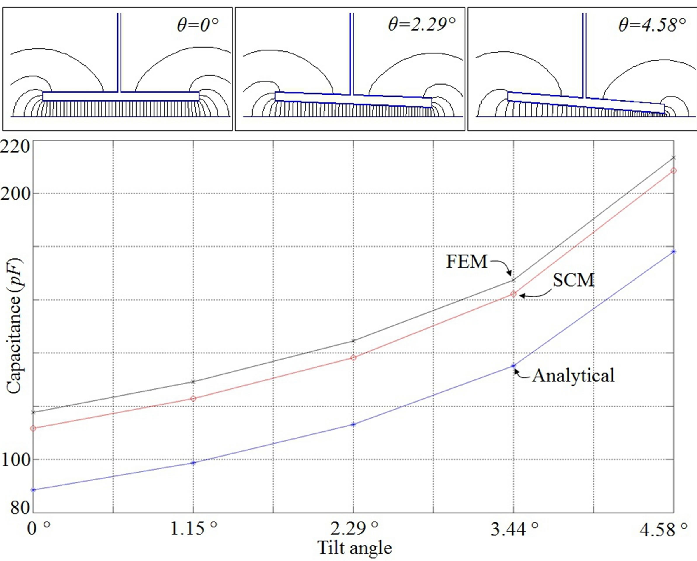
Figure 5. Capacitance results found by three different methods for the MEMS torsional actuator at different deflections. Equation (9) is used to find the analytical results. We set the tolerance as 10-5 when using our SCM-based tool. And we perform the mesh refinement until reaching 0.5% meshing convergence tolerance when using FEM. The analytical results are smaller than both SCM and FEM results because the fringing fields from the side and top surfaces of the proof mass are ignored. The FEM results are slightly larger than the SCM results. This could be caused by the FEM boundary conditions.
4.2. SCM Model
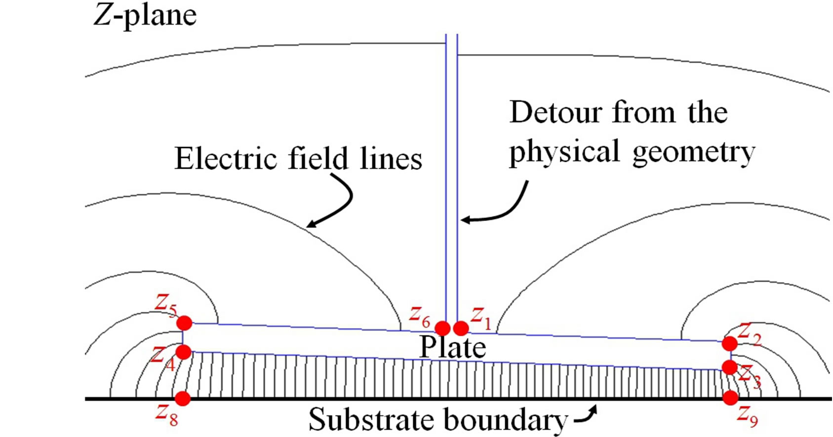
In order to use our tool, there are three working conditions need to be satisfied: 1) The 3D model can be approximated by a 2D model; 2) The 2D model needs to have Dirichlet boundary conditions; and 3) the 2D model can be described by a simply-connected polygon. In Subsection 4.1, we have discussed that the torsional actuator satisfies conditions (1) and (2). In Figuer 6(a), we show the torsional actuator with its vertices in the physical Z-plane. The detailed dimensions of the torsional actuator are listed as: L = 10 µm, h = 0.6 µm, g = 1 µm, and θ = 2.29˚.
 (a)
(a)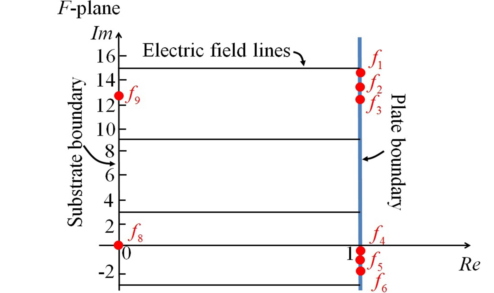 (b)
(b)
Figure 6. SCM-based method for modeling the capacitance of the MEMS torsional actuator. (a) A MEMS torsional actuator with a deflection of θ = 2.29˚ in the physical Zplane is shown. To approximate the torsional plate using a simply-connected polygon, we split the subdomain above the plate with a conductive boundary where charge capacitive charge storage is minimal. The plate has six vertices, and the substrate has two vertices. The boundaries of the detour meet with the substrate boundary at infinity (vertices z7 and z10) from two sides, which is not shown. The plate is at potential V and the substrate is grounded. The electric field lines generated by the tool are shown; (b) We show the mapping onto the strip F-plane. Note that unit length of the real and the imaginary axes are not in scale for better illustration purpose. The eight vertices shown in (a) are mapped onto the F-plane with the same subscript index. The infinity vertices in (a) are mapped to the infinity in the F-plane, which is not shown. The grounded substrate boundary is overlapped with the imaginary axis in the F-plane, and the plate boundary is mapped on a vertical line intersecting with the real axis at 1. The electric field lines, which are not generated by the tool, are for illustration purpose only.
In Figure 6(a), we show the MEMS torsional actuator with a deflection of θ = 2.29˚ in the physical Z-plane. We make the geometry simply-connected by splitting the subdomain above the plate with a conductive boundary where charge storage is minimal. The effect of this detour is verified in Subsection 4.3. The plate has six vertices, and the substrate has two vertices. The boundaries of the detour meet with the substrate boundary at infinity (vertices z7 and z10) from two sides, which is not shown. The plate is at potential V and the substrate is grounded. The electric field lines generated by the tool are shown.
In Figure 6(b), we show the mapping onto the strip Fplane. Note that the unit length of the real and the imaginary axes are not in scale for better illustration purpose. The eight vertices shown in Figure 6(a) are mapped onto the F-plane with the same subscript indices. The infinity vertices in Figure 6(a) are mapped to the infinity in the F-plane, which is not shown. The grounded substrate boundary is overlapped with the imaginary axis in the Fplane, and the plate boundary is mapped on a vertical line intersecting with the real axis at 1. The electric field lines shown in Figure 6(b), which are not generated by the tool, are for illustration purpose only.
The locations of the vertices in the F-plane are found by the SCM MATLAB toolbox with the default tolerance as 10–5. The tolerance determines the accuracy of the numerical algorithm when solving for the locations [12]. We discuss the effects of this tolerance setting to the capacitance result in Subsection 4.4. By using (1), we can calculate the capacitance. For example, the capacitance in the region bounded by the plate boundary, the substrate boundary, and the electric field lines starting at vertices z1 and z6 can be calculated as
 , (10)
where ε is the permittivity of the dielectric between two electrodes, w is the out-of-plane width, and d is the distance between two electrodes in the F-plane which equals to 1 in our tool.
The analytical formula in (9) completely ignores the side and the top surfaces of the torsional actuator. However, the model in our tool accurately accounts for the side and top surfaces, which have significant fringing fields. As expected, the capacitance found by our tool is larger than the capacitance found by (9). For example, the capacitance found by our tool is 18.23% larger than that found by the analytical model when θ = 2.29˚.
4.3. FEM Model
We first use 2D FEM model in COMSOL 3.5a to verify our simply-connected modeling geometry by comparing the simulation results to a model without the geometric detour. We then use a 3D version of the FEM model to verify our 2.5D assumption of the MEMS torsional actuator. We finally discuss the size universe (encompassing subdomain) used in the FEM model.
Our simply-connected version of the geometric configuration from Figure 4 is shown in Figure 6. To create a non-broken polygonal path, we take a detour from the physical geometry at the top center of the plate where not much charge resides. To validate our geometric approximation, we compare two FEM models with and without the geometric detour in Figures 7(a) and (b). Our results indicate that the difference between the two configurations is 4%, where we use ~170,000 meshed elements. In our FEM simulation we use linear finite elements with a mesh density that is refined multiple times until a 0.5% convergence tolerance is reached. That is, we use the relative difference between the capacitance results of the final meshing condition and the previous one for our convergence analysis. We set the boundaries of the plate and the detour at a finite potential, ground the bottom boundary of the universe as the substrate, and set the rest boundaries of the universe as zero charge/symmetry. We find the capacitance by dividing the total charges on the boundaries of the plate by the finite potential we set.
We model the MEMS torsional actuator at deflections of θ = 0˚ and θ = 2.29˚ in both 3D and 2D in COMSOL 3.5a with out-of-plane width, w = 10 µm, which is the same as the plate length. The sizes of the universe in both models are the same. In 3D FEM model, we find the capacitance by dividing the total charges on the plate sur-
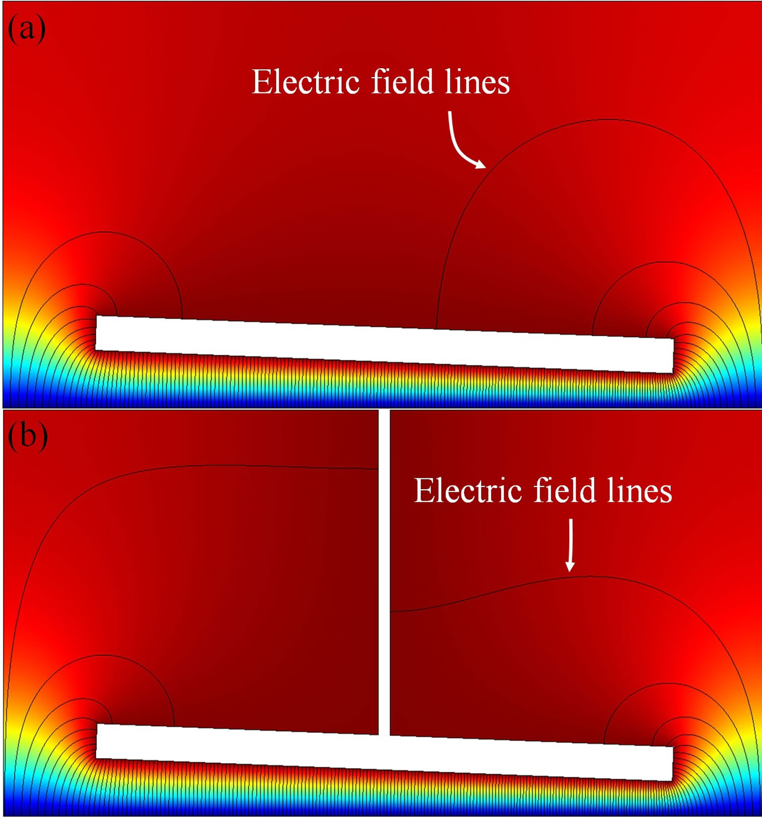
Figure 7. Effect of the boundary detour using FEM-based COMSOL 3.5a. 2D cross section of the torsional actuator without a boundary detour in (a) and with a detour in (b). The relative error of the capacitance between these two configurations is 4%. This evidence supports our use of the detour in our SCM model. The potential field is color mapped, where the torsional plate and boundary detour are at a finite potential, the substrate is grounded, and the other boundaries are set as zero charge/symmetry boundary condition.
faces by the finite potential we set. And in 2D FEM model, we find the capacitance per unit depth first, and find the total capacitance by multiplying the out-of-plane width of the plate. We reach 0.5% and 1.7% convergence tolerance in 2D and 3D models, respectively, on a PC with 4GB memory. We find that the absolute capacitance in 3D model is about 12% larger than those in 2D model at both deflections as expected. This is because the 3D model counts the out-of-plane fringing field. We also find that the change of capacitance between two deflections of 3D model is about 7% larger than that of 2D model. Change of capacitance is typically of more significance to MEMS actuator because it can be used to find the electrostatic actuation force and it is usually less affected by parasitic capacitances.
For FEM models, we find that the capacitance result increases with the increase of the universe size. For example, the capacitance for the MEMS torsional actuator with a deflection of θ = 2.29˚ is 0.35% larger when the universe increases from a 20 µm to a 50 µm one, and the capacitance is 0.21% larger when the universe increases from a 50 µm square to a 100 µm square. In all models, we reach 0.5% convergence tolerance. The decrease of the increasing rate indicates that the effect of the size of the universe to the capacitance decreases as the universe becomes larger. In this paper, we compare our SCM results to the FEM results with a 100 µm-square universe. When the MEMS torsional actuator plate deflects at 2.29˚, the capacitance found by SCM is 4.7% smaller than that found by FEM model. However, computation of capacitance using a larger universe requires more memory and more time. For example, for a universe that is 100 µm-square universe, FEM simulation takes about 1000 times longer than our SCM tool.
Due to the differences between FEM and SCM boundary conditions in modeling the torsional actuator, we perform analysis on a configuration that can be more identically applied to both analyses. In Figure 8, we show our verification results. Here, the center cantilever is at a finite potential; the top, left, and bottom boundaries are grounded; and the right-most boundaries are at infinity for SCM, and zero charge/symmetry boundary conditions for FEM. Although the right-most boundary conditions are slightly different, the equipotential lines are very much alike. The relative error in capacitance is 0.4%, an order of magnitude better than the previous analysis of the torsional actuator configuration.
4.4. Discussion
We discuss the effects of the tolerance parameter in the numerical SCM toolbox to our capacitance results, and compare the capacitance results calculated by three methods.
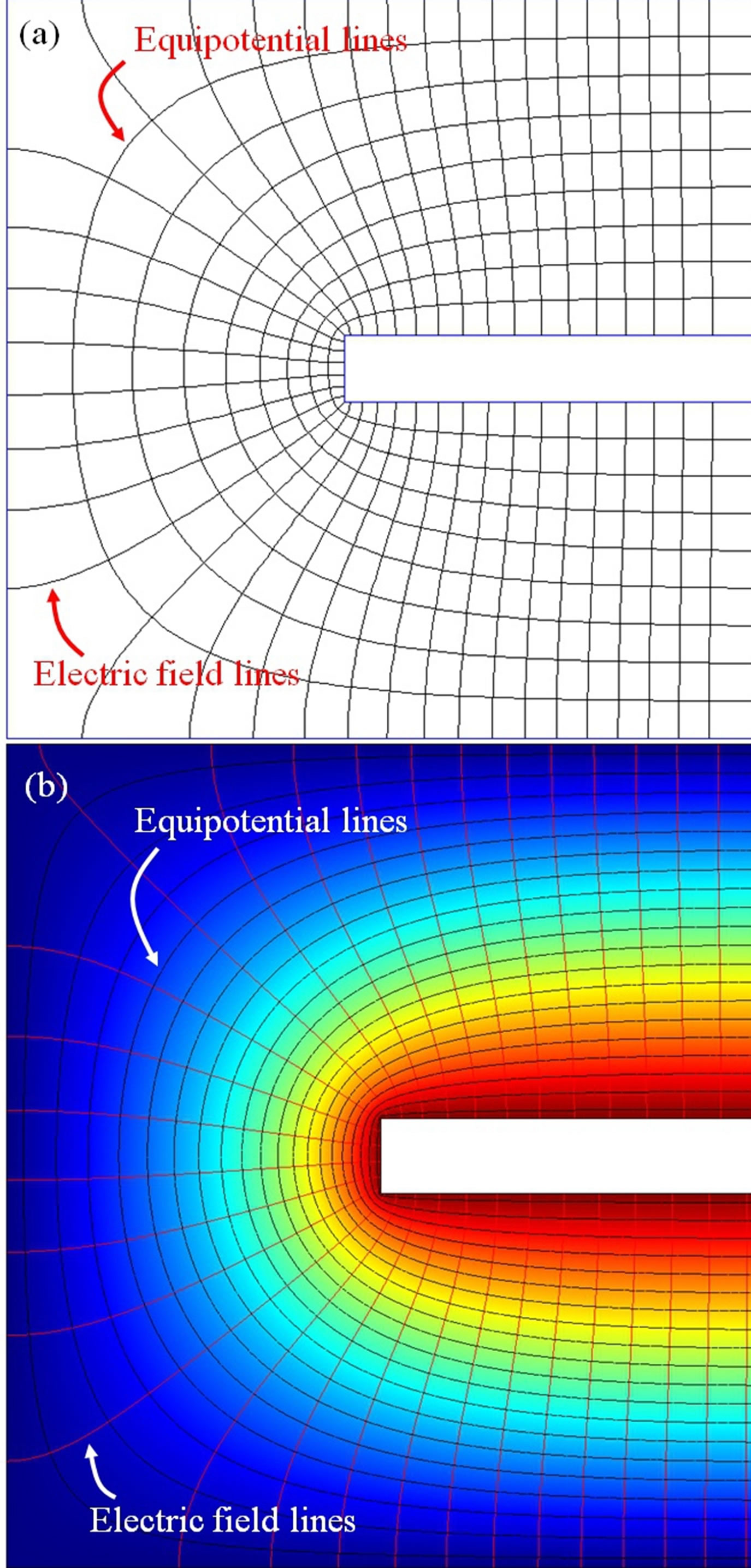
Figure 8. SCM vs. FEM for the same configuration with nearly identical boundary conditions. The center cantilever is at a finite potential; the top, left, and bottom boundaries are grounded; and the right-most boundaries are at infinity for SCM and zero charge/symmetry for FEM. (a) The model is solved by our SCM-based method. We show the equipotential and electric field lines; (b) The model is solved by COMSOL 3.5a. We show the equipotential and electric field lines. The potential is color mapped. Note that the configurations in (a) and (b) have the same geometric dimensions. It appears that they have different dimensions because the scale factors are different in different tools when capturing the images. The relative error between the two capacitance simulations is 0.4%.
In Figure 9, we show the calculated capacitances by using our tool for the torsional actuator with θ = 2.29˚ versus different tolerance settings. The capacitance results approach to 138.2 pF when we reduce the tolerance as expected. We find that the convergence knee occurs when the tolerance is 10–3. That is, the relative difference between the capacitance results is about 0.01% when the tolerance value is less than10–3. The relative difference is defined as the relative change between the capacitance results between two successive tolerance settings.
In Figure 5, we show the capacitance results found by three different methods for the MEMS torsional actuator
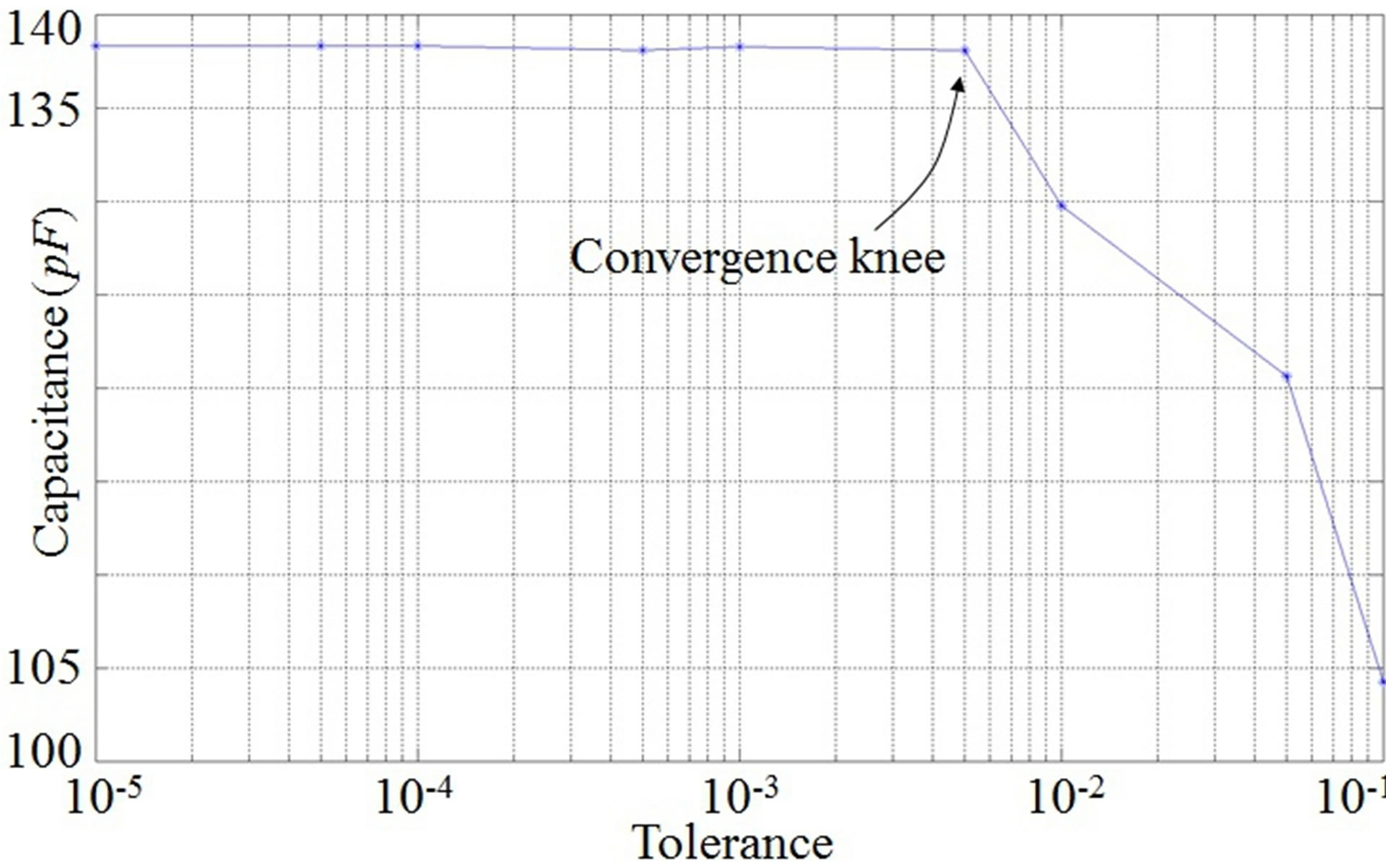
Figure 9. Effects of the tolerance to our capacitance calculations. We show the calculated capacitances by using our SCM tool for the torsional actuator with θ = 2.29˚ versus different tolerance settings in the semilogarithmic plot. We find that the relative difference between the capacitance results is about 0.01% when the tolerance is less than 10–3. The relative difference is defined as the relative change between the capacitance results between two successive tolerance settings.
at different deflections for comparison. We use (9) to find the analytical results, we set the tolerance as 10–5 when using our SCM tool, and we use 100 µm-square universe and perform the mesh refinement until reaching 0.5% meshing convergence tolerance when using the FEM software. The analytical results are smaller than both SCM and FEM results because the fringing fields from the side and top surfaces of the plate are ignored. The FEM results are slightly larger than the SCM results. As discussed in Subsection 4.3, this could be caused by the boundary conditions used in FEM.
5. Conclusion
In this paper, we presented a SCM-based online tool that quickly and accurately calculates the capacitance between two conductors that may be represented as simply-connected polygonal geometries in 2D with Dirichlet boundary conditions. We achieved numerical accuracy by using SCM that treats the fringing fields at vertices exactly. Compared to previous efforts using the SCM, our tools is able to determine the capacitance of a much larger variety of geometries in 2D. We found that by strategically modifying the original geometry on boundaries with the least amount of charge, we are able to obtain good results as verified by FEM. Our tool compares favorably in accuracy to analytical methods, and favorably in both accuracy and speed to the results found by 2D FEM. Using a MEMS torsional actuator as a test case, we find that our SCM tool is about 1000 times faster than FEM. Future research directions might include developing algorithms for calculating other issues such as curve corners and coarse surfaces.
6. Acknowledgements
The authors would like to acknowledge Prof. Driscoll at University of Delaware for insightful discuss on the numerical SCM toolbox. This work was supported by the National Science Foundation Cyber-Enabled Discovery and Innovation and the nanoHUB.
REFERENCES
- V. Kempe, “Inertial MEMS: Principles and Practice,” Cambridge University Press, Cambridge, 2011. doi:10.1017/CBO9780511933899
- V. Kaajakari, “Practical MEMS: Analysis and Design of Microsystems, MEMS Sensors, Electronics, Actuators, RF MEMS, Optical MEMS, and Microfluidic Systems,” Small Gear Publishing, Las Vegas, 2009.
- J. Cheng, J. Zhe and X. Wu, “Analytical and Finite Element Model Pull-In Study of Rigid and Deformable Electrostatic Microactuators,” Journal of Micromechanics and Microengineering, Vol. 14, No. 1, 2004, pp. 57-68. doi:10.1088/0960-1317/14/1/308
- P. S. Sumant, A. C. Cangellaris and N. R. Aluru, “A Conformal Mapping-Based Approach for Fast Two-Dimensional FEM Electrostatic Analysis of MEMS Devices,” International Journal of Numerical Modeling: Electronic Networks, Devices and Fields, Vol. 24, No. 2, 2011, pp. 194-206. doi:10.1002/jnm.770
- K. Nabors and J. White, “FastCap: A Multipole Accelerated 3-D Capacitance Extraction Program,” IEEE Transactions on Computer-Aided Design of Integrated Circuits and Systems, Vol. 10, No. 11, 1991, pp. 1447-1459. doi:10.1109/43.97624
- G. Li and N. Aluru, “A Lagrangian Approach for Quantum-Mechanical Electrostatic Analysis of Deformable Silicon Nanostructures,” Engineering Analysis with Boundary Elements, Vol. 30, No. 11, 2006, pp. 925-939. doi:10.1016/j.enganabound.2006.03.012
- P. Bruschi, A. Nannini, F. Pieri, G. Raffa, B. Vigna and S. Zerbini, “Electrostatic Analysis of a Comb-Finger Actuator with Schwarz-Christoffel Conformal Mapping,” Sensors and Actuators A: Physical, Vol. 113, No. 1, 2004, pp. 106-117. doi:10.1016/j.sna.2004.02.038
- S. He and R. B. Mrad, “Design, Modeling, and Demonstration of a MEMS Repulsive-Force Out-Of-Plane Electrostatic Micro Actuator,” Journal of Microelectromechanical Systems, Vol. 17, No. 3, 2008, pp. 532-547. doi:10.1109/JMEMS.2008.921710
- W. A. Johnson and L. K. Warne, “Electrophysics of Micromechanical Comb Actuators,” Journal of Microelectromechanical Systems, Vol. 4, No. 1, 1995, pp. 49-59. doi:10.1109/84.365370
- J.-L. A. Yeh, C.-Y. Hui and N. C. Tien, “Electrostatic Model for an Asymmetric Combdrive,” Journal of Microelectromechanical System, Vol. 9, No. 1, 2000, pp. 126- 135. doi:10.1109/84.825787
- J. V. Clark, “Electro Micro Metrology,” Ph.D. Thesis, University of California, Berkeley, 2005.
- T. A. Driscoll and L. N. Trefethen, “Schwarz-Christoffel Mapping,” Cambridge University Press, Cambridge, 2002. doi:10.1017/CBO9780511546808
- F. Li and J. V. Clark, “An Online Capacitance Modeling Tool for Conductors That May Be Represented as Simply-Connected Polygonal Geometries in 2.5D,” Nanotech Conference & Exposition, Anaheim, 21-24 June 2010, pp. 557-600.
- A. Jeffrey, “Complex Analysis and Applications,” 2nd Edition, Chapman & Hall, Boca Raton, 2006.
- D. James, “Chipworks inside TI’s DLP Chip,” EE Times Asia, 2006. http://www.eetasia.com/ART_8800416404_1034362_-NT_c232766f.HTM
- J. Kim, H. Choo, L. Lin and R. S. Muller, “Microfabricated Torsional Actuators Using Self-Aligned Plastic Deformation of Silicon,” Journal of Microelectromechanical Systems, Vol. 15, No. 3, 2006, pp. 553-562. doi:10.1109/JMEMS.2006.876789
- D. Hah, E. Yoon and S. Hong, “A Low-Voltage Actuated Micromachined Microwave Switch Using Torsion Springs and Leverage,” IEEE Transactions on Microwave Theory and Techniques, Vol. 48, No. 12, 2000, pp. 2540-2545. doi:10.1109/22.899010
- V. P. Jaecklin, C. Linder, N. F. de Rooij, J.-M. Moret and R. Vuilleumier, “Line-Addressable Torsional Micromirrors for Light Modulator Arrays,” Sensors and Actuators A: Physical, Vol. 41, No. 1-3, 1994, pp. 324-329. doi:10.1016/0924-4247(94)80131-2
NOTES
*Corresponding author.