Journal of Signal and Information Processing
Vol. 4 No. 1 (2013) , Article ID: 28299 , 10 pages DOI:10.4236/jsip.2013.41009
A New Precision Peak Detector/Full-Wave Rectifier
![]()
Department for Electronics, Faculty of Technical Sciences, University of Kragujevac, Kragujevac, Serbia.
Email: predragp@tfc.kg.ac.rs
Received November 4th, 2012; revised December 8th, 2012; accepted December 18th, 2012
Keywords: Dual-Output Current Conveyor (CC); All-Pass Filter; Harmonic Distortion; Precision Peak Detector; Ripple Voltage
ABSTRACT
A new precision peak detector/full-wave rectifier of input sinusoidal signals, based on usage of dual-output current conveyors, is presented in this paper. The circuit gives a DC output voltage that is the peak input voltage over a wide frequency range, with a very low ripple voltage and low harmonic distortion. The proposed circuits use an all-pass filter as a 90˚ phase shifter of the processed input signal. To verify the theoretical analysis, the circuit SPICE simulations results have also been included, showing good agreement with the theory. Inherently, the circuit is well suited for IC implementation.
1. Introduction
Precise full-wave rectification function is one of the important requirements in many applications, such as instrumentation and measurement [1,2]. It is generally used in AC voltmeters and ampermeters, signal-polarity detectors, averaging circuits, sample-and hold circuits, peak value detectors, clipper circuits, and amplitude-modulated signal detectors. In all of these applications, the use of a diode to provide the rectification has the serious drawback of having to overcome the threshold voltage of the diodes. This problem prevents the rectification of signals below a voltage of about 0.6 V. An operational amplifier (OA) with its high open-loop gain can be used to overcome the diode threshold voltage, thereby permitting the rectification of low-level signals. This class of circuit performs generally well at low frequencies but produces moderate to severe waveform distortion at frequencies above about 1 kHz [3]. This occurs due to the fact that the diodes are OFF at the crossover point of the input signal, causing the OA to operate in an open-loop configuration. As the signal frequency increases, slewrate limiting increasingly prevents the OA from turning ON the diodes rapidly and distortion results. It is possible to overcome this problem by the use of a second-generation current conveyor. The current-mode (CM) circuits, such as the second-generation current conveyors CCIIs, have received considerable attention due to their better linearity, wider bandwidth, larger dynamic range, and low power dissipation compared with their voltage-mode counter-parts, such as operational amplifiers (OAs) [3-5].
The CCIIs, first introduced in [6], are functionally flexible and versatile. Thus, they have been used in a very large number of different applications such as universal filters, inductor simulators, capacitance multipliers, oscillators, full-wave rectifiers [7-11]. It is the use of CCIIs, due to high output impendence of the current conveyor, that makes it possible to overcome the turn-on resistance of the diode, permitting the rectification of low-level signals (in most of the cases rectifier was based on usage of diodes) and also responding to frequencies over 100 kHz. The paper [8,10] has extended the frequency range by using voltage and current biasing schemes. While these circuits produce lower distortion and have a wider bandwidth than the OA-based class of circuits, the accuracy is inferior to that of the OA-based circuits. This occurs because of the imprecision of the transfer function, which involves the resistance at the inverting input of each current conveyor. The use of the current conveyor to improve performance of an OA-based circuit was discussed further in [12]. Full-wave rectifiers based on a CMOS class AB amplifier and current rectifier operation are described in [13,14]. This circuit offers a wide dynamic range and shows a broadband operation. CMOS integrated active rectifier concept are an innovative approach for higher efficiencies [15]. These rectifiers provide output voltages nearly at the level of the input voltage combined with low power consumption, which has also been achieved through the circuit design suggested here.
The purpose of a sinusoidal peak detector is to generate a DC output voltage which is proportional to the peak value of the input sinusoidal signal. Due to the waveforms of a power system, voltage and current are sinusoidal. A typical technique to design a peak detector employs, along with filtering circuits, op-amps as the active elements [3,16]. However, it may degrade the transient response of the sinusoidal peak detector. Hence, the transient performance of equipment that uses the typical technique can be improved by using the sinusoidal peak detector with fast transient response [17]. Therefore, the shortcomings are obviously a large configuration but a small operating frequency range and, not less important, a slow response due to the filtering. In this paper, new development of an analogue peak detector is presented with the goal to alleviate the above problems.
In terms of frequency range, the proposed circuit operation covers a wide range of as many as five decades. The proposed circuits compared with the realizations known so far, in terms of ripple voltage and harmonic distortion for the frequency range of 50 Hz−1∙MHz. In addition, the circuit has few passive components. Based on this, it can be concluded that the solution is a highly suitable one for the IC implementation, especially given the fact that the implementation is very straightforward and easy to apply in a number of areas, such as the area of power systems. Computer simulation results, using SPICE program, are given to demonstrate the performance of the proposed peak detector/full-wave rectifier.
2. Proposed Rectification Circuits
The proposed circuit of peak detector is shown in Figure 1.
The circuit consists of five diode-connected MOS transistors, phase shifter, together with two dual-output CCs [18-20]. The NMOS transistors M1, M3 and M5 have a threshold voltage VTn ≥ 0. Similarly, the identical PMOS transistors (M2, M4) have threshold voltage VTp ≤ 0. The Y ports of the CCs are biased at the threshold voltages of the MOS transistors as VB1 = −VTn and VB2 = −VTp (for CCs are vx = vy). The bulks of all of the MOS transistors are connected to their sources.
If  , the current is conducted through the NMOS transistor M1 to the output. However, if
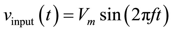
  , the PMOS transistors M2 conducts the current to the output. The M3 and M4 transistors have the same conducting function, each in one of the semi-periods of the phase-shifted input signal. The phase shift of the input signal is realized using an all-pass filter [21,22]. The phase of the input sinusoidal signal:
 (1)
(1)
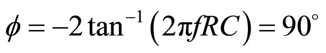
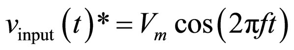
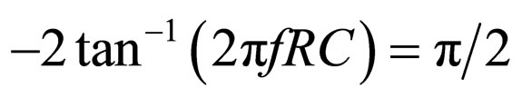
(where Vm is amplitude and f is frequency) is shifted by 90˚ by adjusting the resistance (R) and capacitor (C) of the RC network of the all-pass filter (using AD844) [23] in which the amplitude of the 90˚ phase-shifted signal is kept equal to the amplitude of the input sinusoidal signal. The all-pass filter passes the input signal with unity gain and without attenuation. The use of grounded capacitor is preferred in the integrated circuit (IC) implementation from the aspect of easy fabrication and absorbing parasitic capacitance points. To maintain the phase shift of 90˚ for different frequencies, R and C are adjusted by using the following relation:
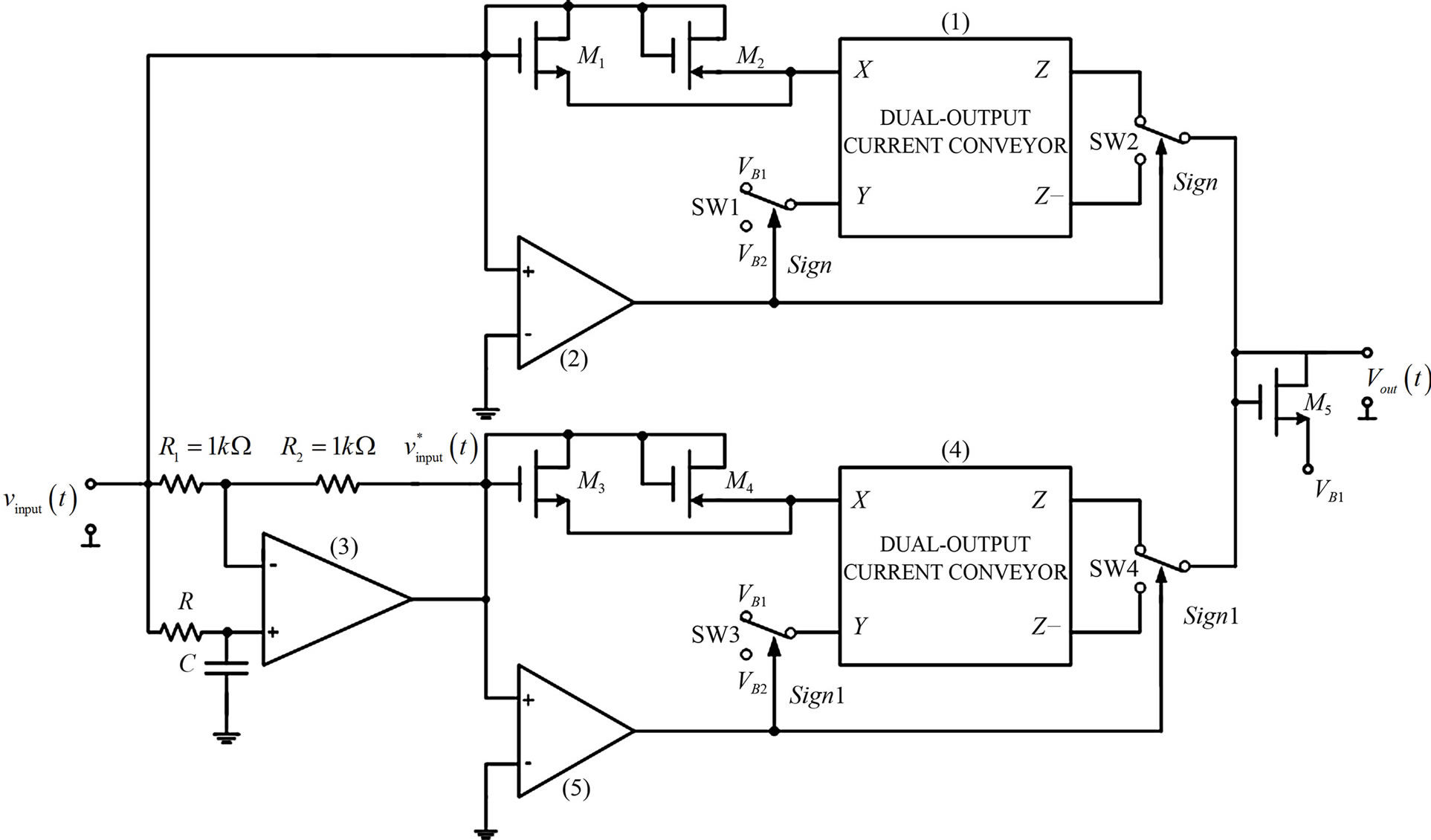
Figure 1. The proposed circuit of peak detector.
 (2)
(2)
The output of the all-pass filter can be written as:
 (3)
(3)
The current-voltage relationships of the used MOS transistors (Figure 1) are given by:
 (4)
(4)
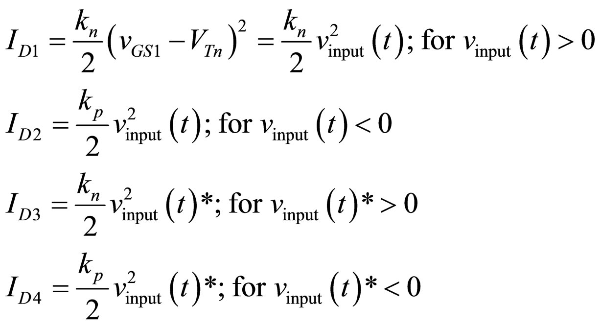
where ID1, ID2, ID3 and ID4 represent the drain currents of the M1, M2, M3 and M4 transistors, respectively. The parameters kn and kp are the transconductance parameters of the NMOS and PMOS transistors, respectively. NMOS and PMOS transistors conduct in opposite halves of the voltage applied on their drains. For dual-output CC,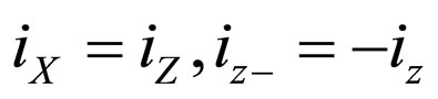 . Depending on the detected sign of the input signals (the control signals Sign and Sign 1), over the comparators (circuits (2) and (5) in Figure 1), the position of the switches SW1 and SW3 can be determined, and the corresponding threshold voltages is connected to Y ports of the dual-output CCs. The corresponding threshold voltage responds to the conducting MOS transistor at this moment. Thus, the relations defined by Equation (4) are satisfied. The control signals Sign and Sign 1, obtained on the output of the comparators, also define the position of the switches SW2 and SW4, and bring the currents either from ports Z, or from ports Z− of the dual-output CCs. Such control enables currents input from the ports Z on the MOS transistor M5 at the interval in which the input voltage signals is positive (voltages
  and
and ), i.e. from the port Z− when the input voltage is negative. Assume that:
 (5)
(5)
for M1, M2, M3, M4 and M5 transistors. For the proposed circuit it follows that:
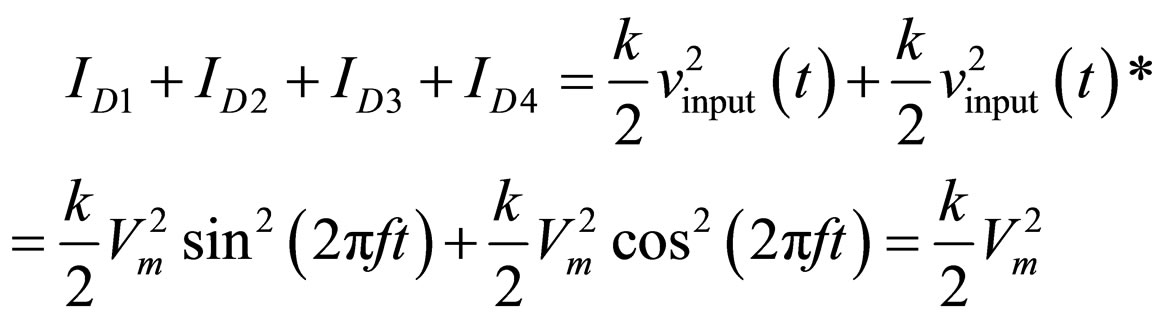 (6)
(6)
The above represents the total current in the Vout node. This current will be equalised with the current of the M5 transistor. It follows that:
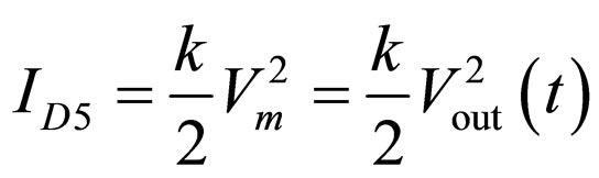 (7)
(7)
From the above, it follows that:
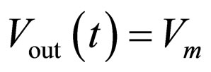 (8)
(8)
Based on (8), it is obvious that the voltage value at the output of the proposed circuit corresponds to the value of the amplitude of the input sinusoid signal. In the proposed circuit, rectification is not performed by diodes, and therefore it has fewer ripples, compared with the known diode rectifier circuits. It is also possible to perform low-voltage (below threshold level of the diode) rectification using the proposed circuit.
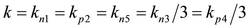
In the above text (proposed circuit in Figure 1), the proposed filter configuration is used primarily due to its simplicity in realization, as well as to the purpose of verifying the proposed concept of processing, with the author being fully aware of all of its limitations. This, most of all, refers to its limited capacities from the aspect of adaptation to the possible change in frequency of the input signal. It is for these reasons that in the continuation of the text, the proposed circuit is a tuneable all-pass filter, offering a practical solution to the problematic RC control via the frequency of input signal, if the proposed circuit is incorporated into a peak detector. The transformation of the input signal (3) is possible to realize using a VM first-order phase shifter with three resistors, one grounded capacitor and two NMOS transistors, as described in [24]. This phase shifter exhibits low sensitivities and good tuneability by using externally controllable electronic resistor. As shown in [24] (relation (8)), the non-inverting phase shifter of this kind makes it possible to effect the required phase shift of 90˚—however, it introduces a 1/3 attenuation of the processed input signal. In order to enable the following described processing, the parameters kn and kp of the NMOS and PMOS transistors M3 and M4 in the proposed circuit in Figure 1 must be adjusted, so that the following condition is applied:
 (9)
(9)
However, if the proposed circuit is implemented in the form of an IC circuit, the realization of the phase shifter makes use (this would be a much more favourable solution) of an all-pass filter (APF) implemented with a second generation current-controlled conveyor (CCCII) [2] and a single capacitor. The realization of the tunable all-pass filter can also be based on one of the already proposed solutions [25-27].
Error Analysis
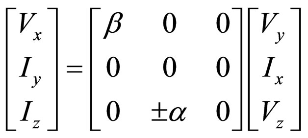
The port relations of the CC can be represented in the matrix form as follows:
 (10)
(10)
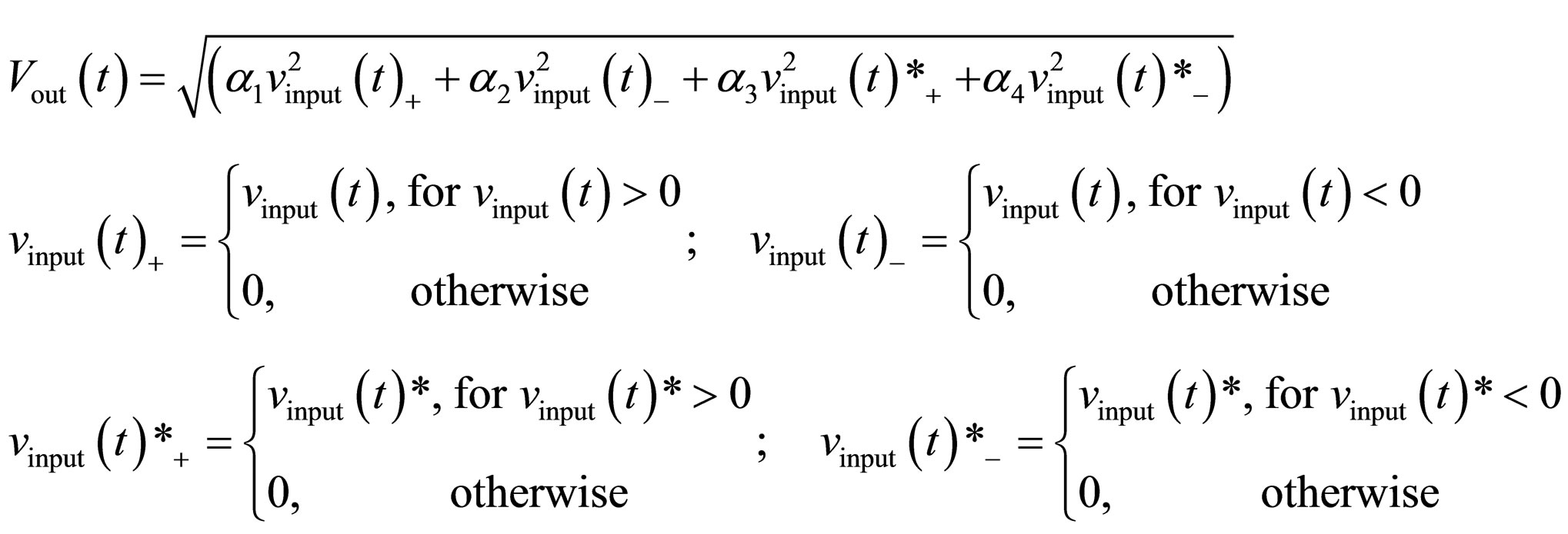
where α and β represent the current and voltage transfer gains of the CC, respectively. The value of the parameters α and β is ideally equal to unity. The + and – signs of α are used for CCII+ and CCII–, respectively. Port X of the CC has a low impendence level, which is ideally zero, whereas the Y and Z nodes show a high impendence level, which is ideally infinity. Taking into account the non-ideal current gains of the CCs α1, α2, α3 and α4 (ignoring the effects of voltage gains); the output voltage (Figure 1) is given by: (Please see the Equation (11) below).
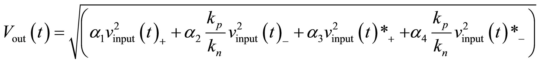
If electronically tuneable CCs (ECCIIs) [28] are employed instead of CCs for the proposed circuit, the parameters α1, α2, α3 and α4 can be used as tools to change the values of the input voltages or to compensate for the error in their values. If (5) is not satisfied, the following inequality is obtained: (Please see the Equation (12) below).
It is observed in (12) that the square of the negative cycles of input signal and 90˚ shifted input signal is multiplied by  instead of unity. Fortunately, using ECCs,
  can be adjusted. It is obvious that the Equation (8) is valid under the ideal condition:
 ;
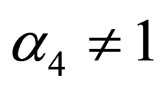
; ; α1 = 1; α2 = 1; α3 = 1; α4 = 1;
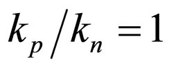 ;
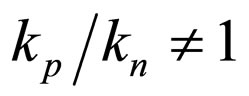
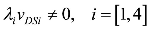
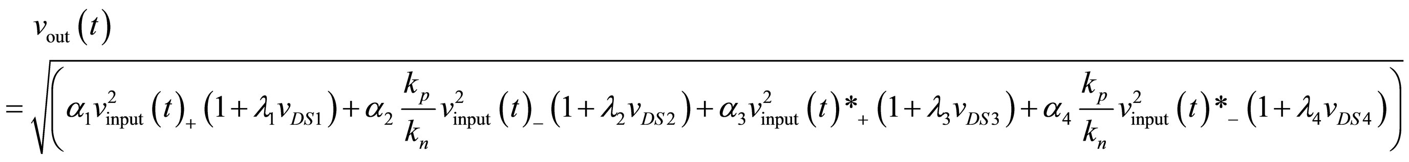
; , where λ, the channel-length modulation parameter, models current dependence on drain voltage due to the Early effect, or channel length modulation. In proposed circuits
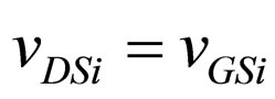 . The output voltage,
  in non-ideal condition becomes: (Please see the Equation (13) below).
A question is raised as of the nature of the output voltage in the proposed detector in circumstances when ideal conditions are not met, i.e. when the time constant 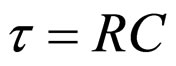 does not fully satisfy the relation
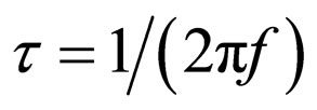 , or if
 ;
; ;
; ;
; ;
; ;
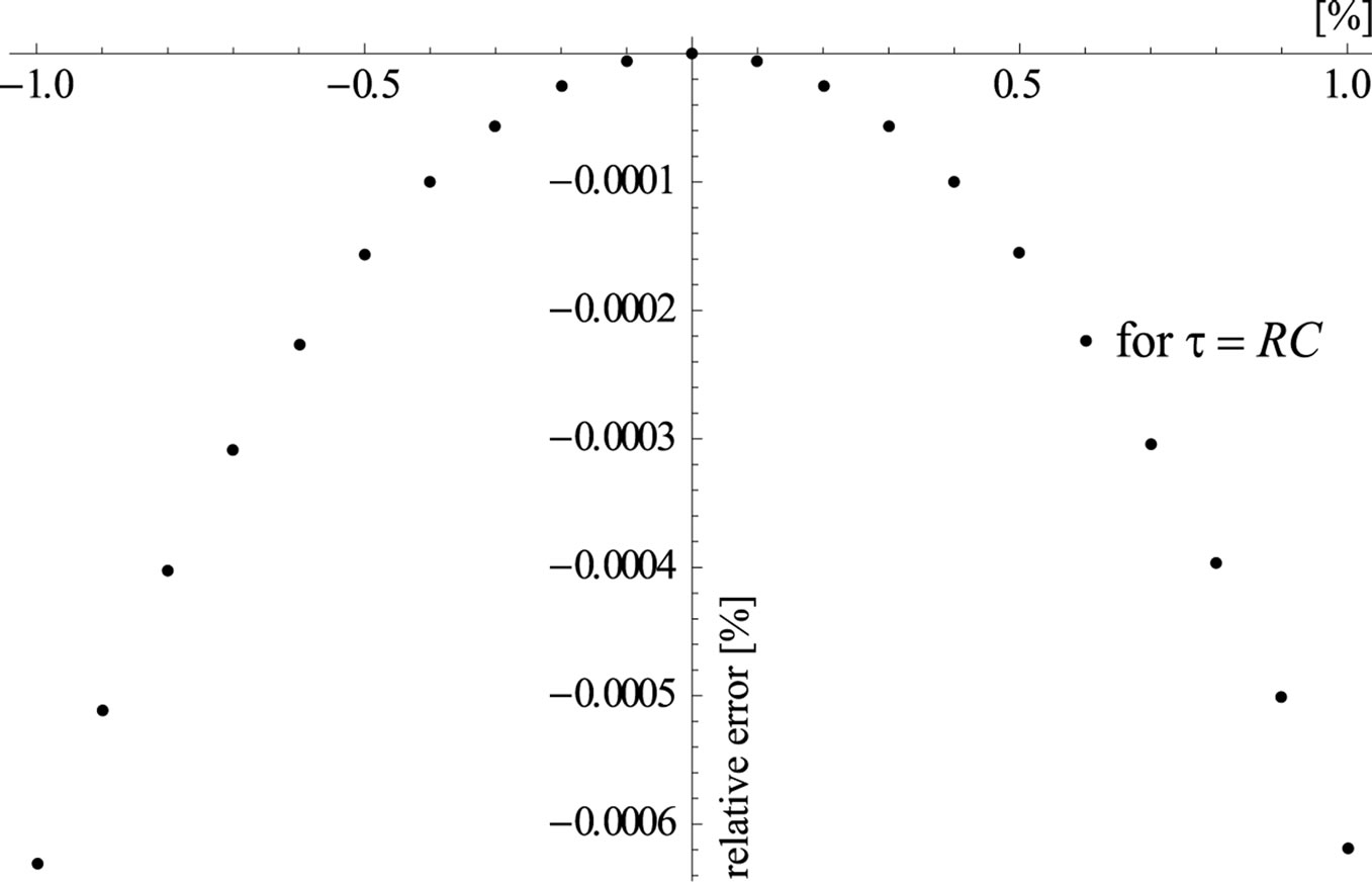
; , i.e. it becomes important to determine the level of sensitivity to the changes in these parameters, within a range bordering with their nominal values. The sensitivity to a change in a parameter will be determined as the first derivative of the output voltage, according to the given (analysed) parameter, Figure 2.
 (a)
(a)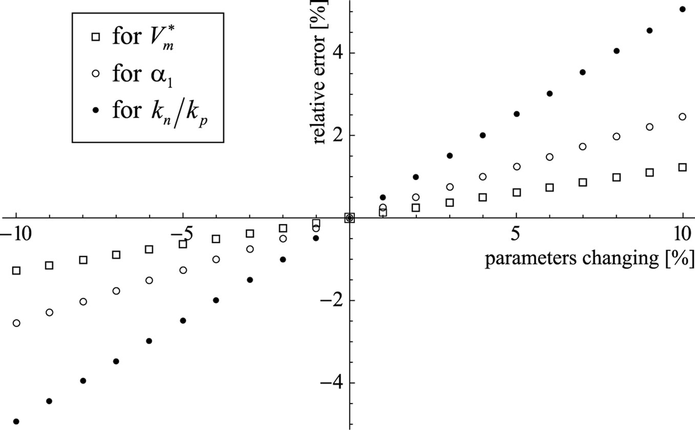 (b)
(b)
Figure 2. Percentage divergence from the exact value of the voltage at the output from the detector, occurring as a consequence of the change in the value of the parameters of the proposed circuit.
 (11)
(11)
 (12)
(12)
 (13)
(13)
If the ideal conditions are not met, then:
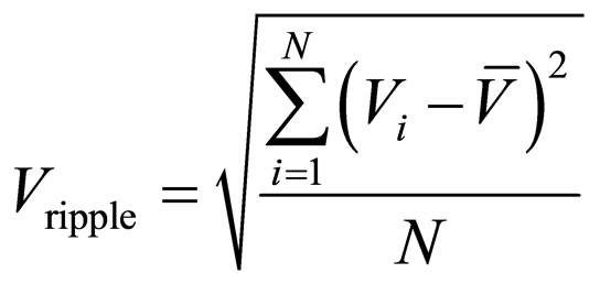
• An alternate component (ripple) will occur, superposed to direct-current voltage at the output. The ripple voltage is obtained from the output waveform of the signal by using the following expression:
 (14)
(14)
where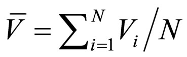 , and
, and  are the output voltages at sampling point
 , respectively. The divergence in the parameter from the nominal, ideal value will cause a ripple in the output signal. The Figures 3 and 4 show the wave-forms of the ripple (two periods), occurring as a result of the divergence of certain parameters by 1%. The frequency of the input signal was assumed to be 50 Hz, determining the scale at the x-axes of the graph (the form of the function is not dependent on the frequency, under the assumptions made). It is assumed that the amplitude of the input signal is 1 V, which also defines the scale at the y-axes.
The dependency of the ripple voltage at the output voltage in the proposed detector to the changes in parameter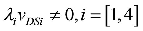 , is similarly as for α (in
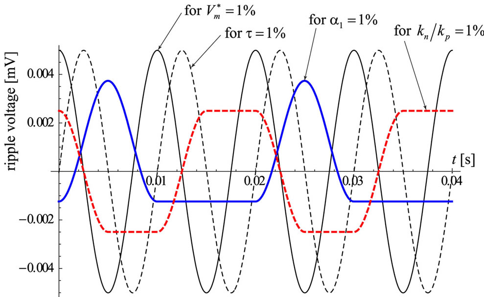
Figure 3. The size of the ripple voltage at the output of the proposed circuit, occurring as a consequence of the variation of the value of individual parameters in the circuit’s elements.
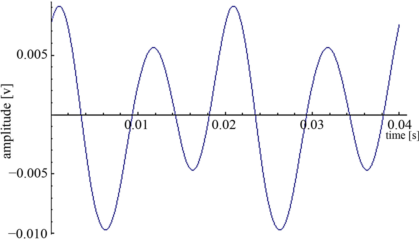
Figure 4. Ripple caused by the 1% shift in all of the parameters (Vpp ≈ 19 Mv; VRMS ≈ 5.5 mV).
same range and has same nature).
• The mean value of the voltage at the output of the detector will no longer equal the amplitude . The mean value
  will be taken as the result of measuring performed in non-ideal conditions, and this value will consequently be compared with the amplitude of the input signal
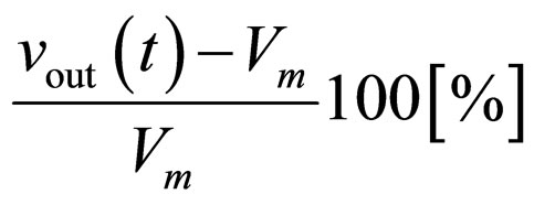
 . The relative error (percentage divergence) is defined as:
 (15)
(15)
Table 1 shows the parameters that are supposed to have the potential of varying around their nominal values: the sensitivity of the result of measuring the amplitude of the input voltage to a change in the circuit parameter; as well as the size of the ripple, occurring as a consequence of these variations. For example, if the parameter  should for any reason be changed by 1% (so that its value becomes
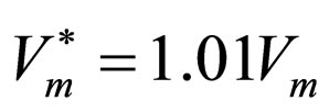 ), the output value (the mean value
 ) will be changed by 0.5% while also-when all the stated parameters are shifted by +1%, an error of 1.6% is obtained.
The situation, in which each parameter fluctuates randomly, at a simultaneous and independent rate, has also been analysed:
• Within the scope ranging from −3% to +3%, with an equal distribution;
• With a Normal distribution (the expected value: 0%, standard divergence: 1%)—this is within the approximate range of the previous even distribution.
The size of the error occurring due to the divergence of the parameters in accordance with the assumed distributions has also been calculated—Figures 5 and 6. For an even distribution, a change in the parameters within the range of −3% to +3% will result in an error that will practically not exceed the value of ±3%.

Table 1. The size of the error in determining the amplitude of the input voltage, which occurs as a consequence of the non-ideal nature of the components applied in the circuit proposed in Figure 1.
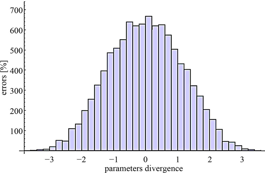
Figure 5. The distribution of errors, for the even distribution of the divergence in the value of the parameters, from their nominal values.
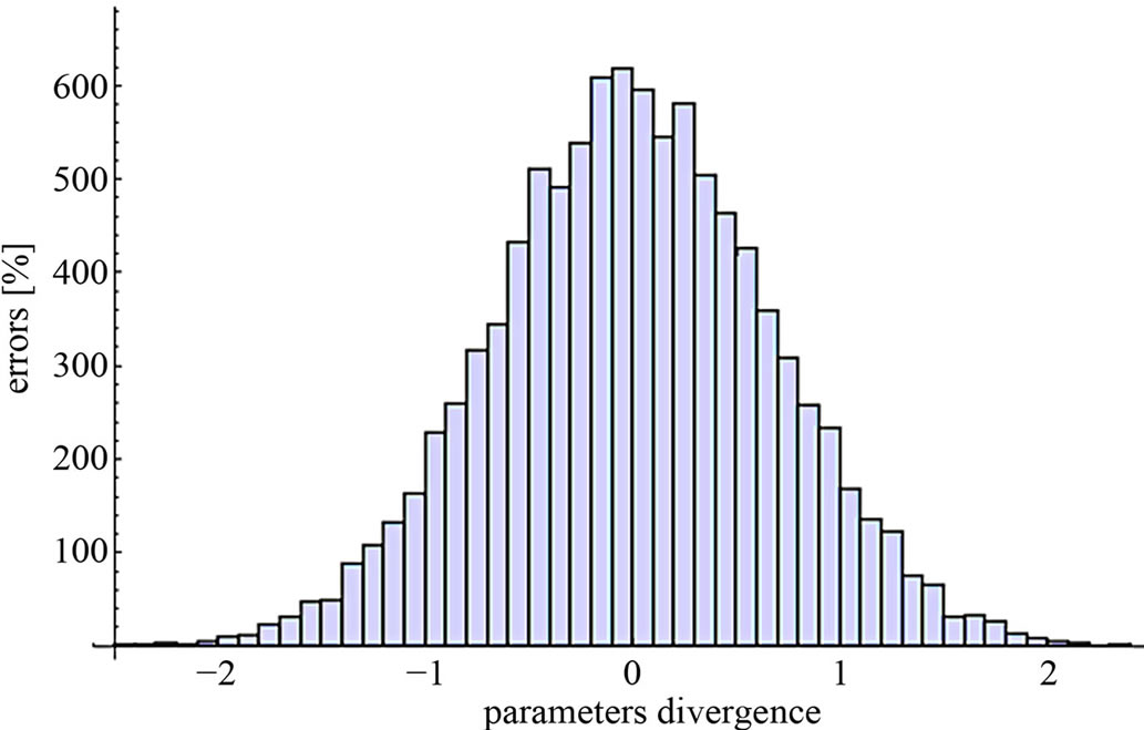
Figure 6. The distribution of errors, for the normal distribution of the divergence in the value of the parameters, from their nominal values.
In the Normal distribution (N(0, 1)), the practical error does not exceed the value of ±2%. The results obtained by simulations and experimental checks have fully confirmed these assumptions.
3. Simulation and Experimental Results
The proposed circuit is simulated using the SPICE program. The MOS transistors in Figure 1 are simulated based on the 0.35-mm Taiwan Semiconductor Manufacturing Company, Limited (TSMC) CMOS technology, with ±1.5 V dc power supply voltages. AD844-type dualoutput CCs with ±15 V dc power supply voltages are used for the circuit implementation [29]. In addition, VB1 = −0.544 V and VB2 = 0.714 V are chosen (these values are specified for the threshold voltages of the chosen MOS transistors). The simulation was conducted using 0.35-mm transistors in order to show that the proposed solution would work for fully integrated systems. This approach was used in publicised papers dealing with the same recent issues [11,14]. The simulation was also performed using CD4007 NMOS and PMOS transistors, in order to allow comparison between the simulation and the experimental results.
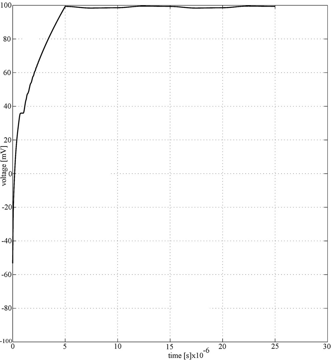
Figure 7 shows the waveform of the proposed circuit for input signals of amplitude 1 V and frequency 50 Hz, and amplitude 100 mV and frequency 100 kHz. As can be seen in Figure 7, it is clear that the theoretical principle sustained the operation in both very low (for applications in power systems) and high frequencies, thus confirming that the proposed method is insensitive to the frequency variation.
From Figures 7(a) and (b) we can conclude that the signal at the output of the proposed circuit contains less ripple voltage in comparison with wave form of the previously reported circuits [13,21,22,30], especially at a higher frequency range. This improvement is due to the absence of peak-value-to-minimum-value variation taking place twice in the output waveform for one cycle, in which one diode conducts for one half cycle and other diode conducts for the other half cycle. The proposed solution also enables performing low-voltage rectification (below threshold level of the diode).
The DC characteristics of the proposed circuit for a lower frequency of 50 Hz and a high frequency of 100 kHz are shown on Figure 8. It was taken R = 1.59 MW and C = 0.002 mF at f = 50 Hz, and R = 796 W and C = 0.002 mF at f = 100 kHz to maintain a 90˚ phase shift of the all-pass filter [21,22]. Based on Figure 8, it can be concluded that the proposed circuit retains a linear character in a wide frequency range, much better that circuits reported in [13,15,31].
3.1. Ripple Voltage
For better performance of a rectifier, the value of the ripple should be very low [21,22]. Based on the obtained results, Figure 9, the ripple voltage of the proposed circuit is much lower than in previously reported circuits of rectifiers [13,22,23,30,32]. For the proposed circuit, with an input signal of 100 mV, it was obtained a low ripple voltage of 0.45 mV at 50 Hz and 0.81 mV at 1 MHz. With an input voltage of 1 V amplitude, the ripple voltages are obtained as 1.6 mV at 50 Hz and 4.6 mV at 1 MHz.
3.2. Harmonic Distortion
A further indication of the performance of each of the full-wave rectifiers can be gleaned by examining the distortion already present in a full-wave rectified signal. When a sinusoidal signal of frequency f is applied to a full-wave rectifier, the steady-state response at the output ideally consists of harmonic components at 2f, 4f, 6f, etc. The harmonics in the signal causes the distortion in the output of the circuit. Because of its periodic nature, these harmonic components can be analyzed by the Fourier
 (a)
(a)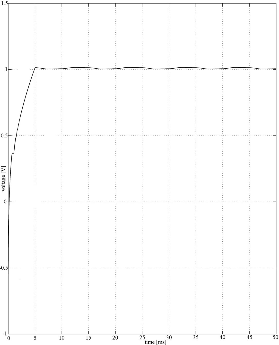 (b)
(b)
Figure 7. The rectified output waveforms of the proposed circuit (a) for input amplitude voltage of 100 mV at 100 kHz; (b) for input amplitude voltage of 1 V at 50 Hz.

Figure 8. DC output voltage versus DC input voltage.
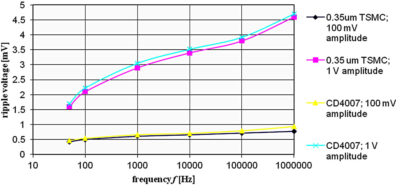
Figure 9. Ripple voltage versus frequency curve for the proposed circuit.
series. The magnitude of each harmonic of a waveform as shown in Figure 10 is obtained with fast Fourier transform using PSPICE.
The total harmonic distortion, or THD, of a signal is a measurement of the harmonic distortion present and is defined as the ratio of the sum of the powers of all harmonic components to the power of the fundamental frequency:
 (16)
(16)
where V1 is fundamental frequency voltage content, Vn is nth harmonic voltage content, and 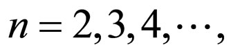 etc. In the case of a full-wave rectifier, the steady-state response at the output consists of even harmonics.
Figure 10 shows the total harmonic distortion of the output voltage of the proposed circuit, Figure 1. The THD of the proposed circuit is −16.5 dB at 50 Hz and −21 dB at 1 MHz with an input signal of 1 V. The THD is much lower than in [21,22,32] (the THD of previously reported circuit slowly increases with frequency), because for higher frequency ranges, the switching ON and OFF of diodes becomes sluggish due to its higher impendence and more distortions.
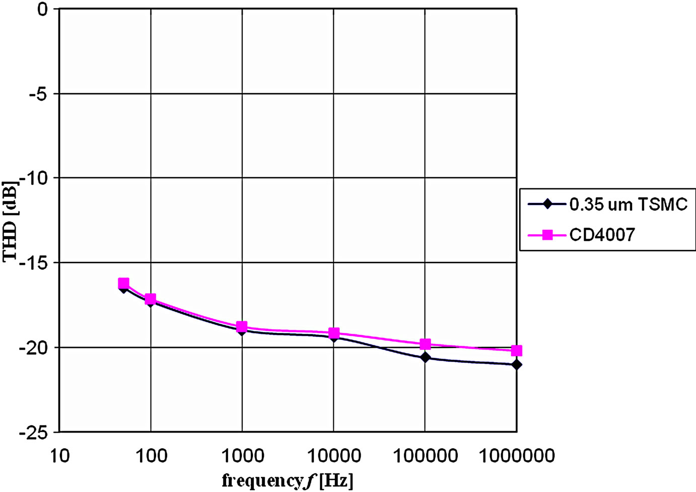
Figure 10. Total harmonic distortion (THD) versus frequency at input amplitude voltage of 1 V.
3.3. Experimental Results
The experimental test for the peak detector (full-wave rectifier) in Figure 1 is performed by using CD 4007 MOS array transistors and AD844s integrated circuit (Analog Devices) as CCs. The dc power supply for AD844s is chosen to be ±15 V, the biasing voltage VB is selected to be equal to −1.77 V (negative of the threshold voltage of the employed NMOS transistors). The input sinusoidal voltage with a 1 V peak at 10 kHz is applied to the rectifier. Figure 11(a) represents the signal of 90˚ phase shift with the input signal. Figure 11(b) shows the rectified output waveform of voltage ~0.98 V. The experimental value of the ripple voltage is obtained as ~8 mV by using (13) from the Figure 11(b). The difference between the experimental and theoretical values of ripples shown in Figure 9 may be due to deviation of the design parameters such as the R, C, and input impendence of the ICs used in the circuit from its experimental values.
In the conducted experimental procedure, the diodes being able to have the bulks tied separately. If the proposed circuit is incorporated in a technical device, an occurrence of considerably bulk current resulting from hot carrier effects could be expected (the generated majority carriers create a bulk current). Since most of the current generated in this way has a direct impact on the lifetime of MOS transistors, it is a major concern to keep the bulk current as low as possible. Bulk currents are comparatively unimportant as long as the parasitic series resistance of the bulk does not establish a drastically increased bulk potential which can lead to threshold voltage reduction or even more serious effects like snap-back or latch-up. It is however possible to reduce this current. The paper [33] describes a number of circuit optimization techniques for controlling the standby leakage current, including power gating and body bias control. The paper presents techniques for active leakage control, including use of multiple-threshold cells, long channel devices, input vector design, transistor stacking to switching noise, and sizing with simultaneous threshold and supply voltage assignment. A high efficient latch-up current self-stop methodology and circuit for whole-chip latch-up prevention have been proposed in [34]. By implementing this simple circuit with only a small area, bulk CMOS IC products can be designated free to latchup damage.
 (a)
(a)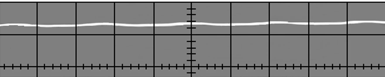 (b)
(b)
Figure 11. Experimental results for the full-wave rectifier in Figure 1 for a 1 V peak input voltage (vertical scale: 0.75 V/division; horizontal scale: 42 ms/division). (a) 90˚ phase shifted signal with input signal; (b) Rectified output signal.
4. Conclusion
In this paper, a new precision peak detector (full-wave rectifier) of input sinusoidal signals, which employs two dual-output CCs and five MOSFETs using an all-pass filter as a 90˚ phase shifter, is presented. The technique offers several advantages which support the IC implementation. All these elements will lead to reduced costs of the suggested solution. The circuit provides linear variation of the dc output voltage with the input voltage, with the output voltage amplitude being almost the same as the peak input voltage over a frequency range of 50 Hz to 1 MHz. The simulation results confirm the theory well. The ripple and THD of the output voltage of the proposed circuit is much lower than in previously realized rectifiers. The proposed circuit has high precision, wide bandwidth, and high accuracy.
5. Acknowledgements
The author wishes to thank to the Ministry of Education and Science of the Republic of Serbia for its support of this work provided within the projects 42009 and OI- 172057.
REFERENCES
- R. Coughlin and F. Driscoll, “Operational Amplifiers and Linear Integrated Circuits,” 3rd Edition, Prentice-Hall, Englewood Cliffs, 1987.
- P. Gray, P. J. Hurs, S. H. Lewis and R. G. Meyer, “Analysis and Design of Analog Integrated Circuits,” Wiley, New York, 2001.
- C. Toumazou, F. J. Lidgey and D. G. Haigh, “Analog IC Design: The Current-Mode Approach,” Peregrinus, London, 1990.
- B. Wilson, “Recent Developments in Current Conveyors and Current-Mode Circuits,” IEEE Proceedings G Circuits, Devices and Systems, Vol. 137, No. 2, 1990, pp. 63-77.
- B. Wilson, “Trends in Current Conveyor and CurrentMode Amplifier Design,” International Journal of Electronics, Vol. 73, No. 3, 1992, pp. 573-583. doi:10.1080/00207219208925692
- A. S. Sedra and K. C. Smith, “A Second-Generation Current Conveyor and Its Applications,” IEEE Transactions on Circuit Theory, Vol. 17, No. 1, 1970, pp. 132-134. doi:10.1109/TCT.1970.1083067
- A. Monpapassorn, K. Dejhan and F. Cheevasuvit, “A Full-Wave Rectifier Using a Current Conveyor and Current Mirrors,” International Journal of Electronics, Vol. 88, No. 7, 2001, pp. 751-758. doi:10.1080/00207210110052892
- C. Toumazou, F. J. Lidgey and S. Chattong, “High Frequency Current Conveyor Precision Full-Wave Rectifier,” Electronics Letters, Vol. 30, No. 10, 1994, pp. 745-746. doi:10.1049/el:19940539
- D. Stiurca, “Truly Temperature Independent Current Conveyor Precision Rectifier,” Electronics Letters, Vol. 31, No. 16, 1995, pp. 1302-1303. doi:10.1049/el:19950905
- K. Hayatleh, S. Porta and F. J. Lidgey, “Temperature Independent Current Conveyor Precision Rectifier,” Electronics Letters, Vol. 30, No. 25, 1994, pp. 2091-2093. doi:10.1049/el:19941454
- E. Yuce, S. Minaei and O. Cicekoglu, “Full-Wave Rectifier Realization Using Only Two CCII+s and NMOS Transistors,” International Journal of Electronics, Vol. 93, No. 8, 2006, pp. 533-541.
- S. J. Gift, “A High-Performance Full-Wave Rectifier Circuit,” International Journal of Electronics, Vol. 87, No. 8, 2000, pp. 925-930. doi:10.1080/002072100404587
- J. R. Angulo, R. G. Carvajal, J. M. Heredia and A. Torrabla, “Very Low-Voltage Class AB CMOS Precision Voltage and Current Rectifier,” Proceedings of IEEE International Symposium on Circuits and Systems, Vol. 3, 2000, pp. 5-8.
- A. V. Garcia, R. Venkatasubramanian, J. S. Martimez and E. S. Sinencio, “A Broadband CMOS Amplitude Detector for On-Chip RF Measurements,” IEEE Transactions on Instrumentation and Measurement, Vol. 57, No. 7, 2008, pp. 1470-1477. doi:10.1109/TIM.2008.917196
- C. Peters, J. Handwerker, D. Maurath and Y. Manoli, “A Sub-500 mV Highly Efficient Active Rectifier for Energy Harvesting Applications,” IEEE Transactions on Circuits and Systems I: Regular Papers, Vol. 58, No. 7, 2011, pp. 1542-1550.
- W. D. Stanley, “Operational Amplifiers with Linear Integrated Circuits,” 4th Edition, Prentice Hall, Upper Saddle River, 2002.
- C. T. Pan and M. C. Jiang, “A Quick Response Peak Detector for Variable Frequency Three-Phase Sinusoidal Signal”, IEEE Transactions on Industrial Electronics, Vol. 41, No. 4, 1993, pp. 2003-2008.
- K. Pal, “Modified Current Conveyors and Their Applications,” Microelectronics Journal, Vol. 20, No. 4, 1989, pp. 37-40. doi:10.1016/0026-2692(89)90076-1
- A. M. Soliman, “Modified Current Conveyor Filters: Clasification and Review,” Microelectronics Journal, Vol. 29, No. 3, 1998, pp. 133-149. doi:10.1016/S0026-2692(97)00080-3
- W. Tangsrirat and W. Surakampontorn, “High Output Impendance Current-Mode Universal Filter Employong Dual-Output Current-Controllled Conveyors and Grounded Capacitors,” AEU International Joural of Electronics and Communications, Vol. 61, No. 2, 2007, pp. 127-131.
- P. P. Sahu, M. Singh and A. Baishya, “A Novel Versatile Precision Full-Wave Rectifier,” IEEE Transactions on Instrumentation and Measurement, Vol. 59, No. 10, 2010, pp. 2742-2746. doi:10.1109/TIM.2010.2045539
- P. P. Sahu, M. Singh and A. Baishya, “New Low-Voltage Full Wave Rectification Technique without a Diode,” IET Circuits, Devices & Systems, Vol. 5, No. 1, 2011, pp. 33-36.
- R. A. Gayakwad, “Op-Amps and Linear Integrated Circuits,” 3rd Edition, Prentice-Hall, New Delhi, 2007, pp. 316-318.
- E. Yuce and S. Minaei, “A Novel Phase Shifter Using Two NMOS Transistors and Passive Elements,” Analog Integrated Circuits and Signal Processing, Vol. 62, No. 1, 2010, pp. 77-81. doi:10.1007/s10470-009-9324-8
- A. Toker and S. Ozoguz, “Tunable Allpass Filter for Low Voltage Operation,” Electronics Letters, Vol. 39, No. 2, 2003, pp. 175-176. doi:10.1049/el:20030179
- S. Na Songkla and W. Jaikla, “Realization of Electronically Tunable Current-Mode Fist-Order Allpass Filter and Its Application,” T. World Academy of Science, Engineering and Technology, Vol. 61, 2012, pp. 410-413.
- B. Metin and O. Cicekoglu, “Tunable All-Pass Filter with a Single Inverting Voltage Buffer,” Proceedings of Research in Microelectronics and Electronics, 2008, pp. 261-263.
- S. Minaei, O. K. Sayin and H. Kuntman, “A New CMOS Electronically Tuneable Current Conveyor and Its Application to Current-Mode Filters,” IEEE Transactions on Circuits and Systems I: Regular Papers, Vol. 53, No. 7, 2006, pp. 1448-1457. doi:10.1109/TCSI.2006.875184
- S. Rana and K. Pal, “Current Conveyor Simulation Circuits Using Operational Amplifiers,” Journal of Physical Science, Vol. 11, 2007, pp. 124-132.
- S. J. Gift and B. Maudy, “Versatile Precision Full-Wave Rectifiers for Instrumentation and Measurement,” IEEE Transactions on Instrumentation and Measurement, Vol. 56, No. 5, 2007, pp. 1703-1710. doi:10.1109/TIM.2007.904565
- P. Walker and M. Green, “CMOS Half-Wave and Full Wave Precision Voltage Rectification Circuits,” Proceedings of the 38th Midwest Symposium on Circuits and Systems, Vol. 2, 1995, pp. 901-904.
- Z. Wang, “Novel Pseudo RMS Current Converter for Sinusoidal Signals Using a CMOS Precision Current Rectifier,” IEEE Transactions on Instrumentation and Measurement, Vol. 39, No. 4, 1990, pp. 670-671. doi:10.1109/19.57256
- F. Fallah and M. Pedram, “Standby and Active Leakage Current Control and Minimization in CMOS VLSI Circuits,” IEICE Transactions on Electronics, Vol. E88-C, No. 4, 2005, pp. 509-519. doi:10.1093/ietele/e88-c.4.509
- J. J. Peng, M. D. Ker and H. C. Jiang, “Latchup Current Self-Stop Circuit for Whole-Chip Latchup Prevention in Bulk CMOS Integrated Circuits,” Proceedings of IEEE International Symposium on Circuits and Systems, Vol. 5, 2002, pp. 537-540.