Advances in Materials Physics and Chemistry
Vol. 2 No. 1 (2012) , Article ID: 17902 , 4 pages DOI:10.4236/ampc.2012.21009
Study the Effect of Irradiation Time and HF Concentration on Porosity of Porous Silicon and Study Some of the Electrical Properties of Its Based Device
Physics Department, College of Science, University of Baghdad, Baghdad, Iraq
Email: nathera_2007@yahoo.com
Received November 20, 2011; revised December 28, 2011; accepted January 9, 2012
Keywords: Porous Silicon; Photochemical Process; Porosity; Structural Properties; Porosity; Electrical Properties
ABSTRACT
Porous silicon has been produced in this work by photochemical etching process (PC). The irradiation has been achieved using ordinary light source (150d250 W) power and (875 nm) wavelength. The influence of various irradiation times and HF concentration on porosity of PSi material was investigated by depending on gravimetric measurements. The I-V and C-V characteristics for CdS/PSi structure have been investigated in this work too.
1. Introduction
Porous silicon (PSi) can be considered as a silicon crystal having a network of voids in it .The nanosized voids in the silicon bulk result in a sponge—like structure of pores and channels surrounded with a skeleton of crystalline silicon nanowires [1].
The interest in porous silicon has increased greatly over the last decades, mainly due to its photoluminescence properties and the potential applications, which arise from these [2,3]. There are, however, many other possible uses including chemical sensors, micromachining, micro scale optical components, and filters and diffraction grating. Porous silicon is usually prepared by iodization in aqueous hydrogen fluoride (HF). It is also possible to employ a photochemical technique, which does not involve an externally applied bias [2]. According to G. Lerondel et al., porosity is defined as the fraction of void within the PSi layer and can be easily determined by weight measurements. This macroscopic characteristic can be measured by gravimetry, preferably on thick layers. The accessible porous silicon values typically included between 15% and 90%. It is significant to note that porosity is an average value and that for the same porosity; various material morphologies can be obtained [4].
2. Experimental Work
Commercially available n-type (111) oriented silicon wafers of (500 ± 15 µm) thickness with resistivity (r = 3.84 × 10⁵ W∙cm) have been used as substrate. Before the photochemical etching process, the silicon wafer has been cut out into small pieces in dimensions of (0.5 × 0.5 cm). After the cleaning, the silicon wafers were immersed in hydrofluoric acid (HF) aqueous solution. The HF concentration was changed in the range (24 to 36 wt%). All samples were front-side illuminated using a Halogen lamps of power density (0.28 & 0.7 W/cm2). The sample has been mounted on a Teflon cell in such away that the current required for the etching process, could pass from bottom surface to the top of the polished surface through the electrolyte. The light source was vertically aligned and focused by quartz lens of (3.87 cm) focal length.
The porosity of PSi layers has been determined by using the gravimetric method according to the following equation [4]:
 (1)
(1)
where g is the porosity, m1 and m2 are the weight of the silicon substrate before and after the etching process respectively, and m3 is the weight after removing the porous silicon layer.
The fabricated CdS/PSi junction was achieved by using the chemical spray pyrolysis technique.
3. Results and Discussion
Figure 1 shows the relationship between porosity and etching time of prepared PSi layer at different irradiation time (30 - 90 min), 24% HF concentration, and power density of 0.28 W/cm2. From this figure, we can see that the values of porosity are increasing with increasing of etching time. This result is ascribed to the increasing of the number and width of the pores with increasing of etching time. Our result agrees with outcomes of [1,5].
Also, Figure 2 represents the relationship between porosity and HF concentration (24 - 36 wt%), etching time (60 min), and power density of 0.7 W/cm2. We can observe from this figure that the porosity decreases with increasing HF concentration. By lowering HF the porosity of the substrate is raised until there is enough HF serving F– ion in the electrolyte. This is necessary to oxidize Si and provide charge carriers for the electrolysis. This result is comparable with result of [6].
Figure 3 shows the I-V characteristics for CdS/PSi heterojunction at dark and reverse bias at room temperature, at etching time (30 min), 24% HF concentration, and power density of (0.28 W/cm2). In general, the forward dark current is generated due to the flow of majority carriers and the applied voltage inject majority carriers which leads to decrease the value of built—in potential, and decrease the width of the depletion layer. Then majority and minority carrier concentration is higher than

Figure 1. The relation between porosity and etching time.
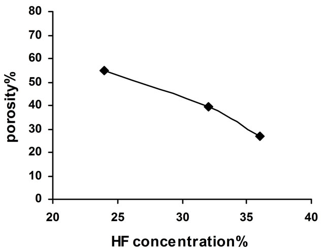
Figure 2. The relation between porosity and HF concentration.
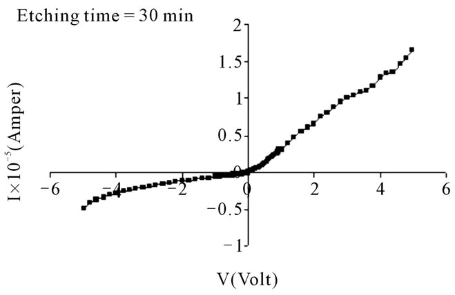
Figure 3. The I-V characteristics at dark for CdS/PSi HJ.
the intrinsic carriers concentration (ni < np) which leads to generate recombination current at the low voltage region because that the excitation electrons from V.B to C.B will recombine with the holes which found at the V.B, and this is observed by increasing in recombination current at low voltage region.
While the tunneling current is observed at high voltage region. After that, there is a fast exponential increase in the current magnitude with increasing the voltage and this is called diffusion current, which is dominated [7].
Also, the reverse bias current contains two regions in the voltage region the current increases with increasing the applied voltage, and the generation current dominates. At the high voltage region, the current is stabilizes and becomes independent of the bias potential, this is called the diffusion current [8,9].
Also, the current-voltage characteristics exhibit rectification behavior may be due to the hetrojunction potential barrier at the CdS/PSi interface [10]. The rectification factor indicates the ratio between forward and reverse current at a certain applied bias voltage.
Figure 4 represents I-V characteristics under illumination with different power intensities (69.19 and 182.9 mW/cm2) at room temperature of the CdS/PSi HJ, containing PSi layers prepared at etching time (30 min), 24% HF concentration and for power density (0.24 W/cm2).
The photocurrent has been observed in reverse bias only, and we can see from this figure, that the presence of the light illumination strongly increases the reverse current.
The photocurrent is always in the reverse bias direction due to it increases by increasing the depletion region width. The increasing of the reverse bias voltage leads to the increase in the internal electric field which leads to an increasing in the probability of the separated electron— hole pairs. The photocurrent increases with increasing the incident power intensity, due to the increasing in the number of the generated photo carriers in the depletion region with the diffusion depth for carriers which depends on the life time of the minority carriers on the two sides of the depletion region [11].
The capacitance—voltage characteristics have been studied in this work. The variation of capacitance as a function of reverse bias voltage for CdS/PSi HJ which contains PSi layer prepared at etching time (30 min) is shown in Figure 5. It is observed from this figure that the capacitance decreases with increasing the reverse bias. This decreasing was unexponential, that the capacitance becomes constant approximately at high voltages. This behavior was attributed to the increasing in the depletion region width which leading to the increasing of built—in voltage [7].
The relation between inverse capacitance squared against the reverse bias at 30 min etching time is shown in Figure 6. This exponential relationship represents that the junction was an abrupt type. According to the capacitance—voltage measurements, the capacitance, the built—in voltage, the width of the depletion layer and the carriers’ concentration are equal to 48 × 10–12 F, 0.4 V, 0.077 µm, and 0.35 × 1018 cm–3 respectively.
4. Conclusion
The porosity of PSi layer increases with increasing etching time. And it’s decreased with the increasing of HF concentration. Also, the current-voltage characteristics
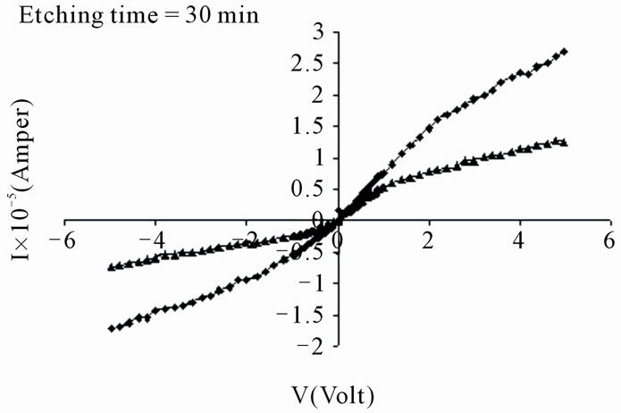
Figure 4. The I-V characteristics under illumination for CdS/PSi HJ.
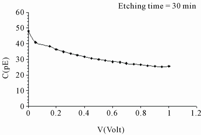
Figure 5. The variation of capacitance as a function of reverse bias voltage for CdS/PSi HJ.
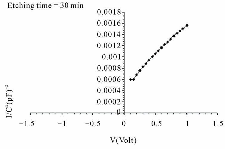
Figure 6. The variation of 1/C2 as a function of reverse bias voltage for CdS/PSi HJ.
exhibit rectification behavior may be due to the hetro junction potential barrier at the CdS/PSi interface. The photocurrent increases with increasing the incident power intensity. The relationship between inverse capacitance squared and the reverse bias represents that the junction was abrupt type. The chemical deposition of CdS thin film on porous silicon layer offers wide applications of low-cost solar cells and detectors in hetrojunction structures.
REFERENCES
- L. T. Canham, “Silicon Quantum Wire Array Fabrication by Electrochemical and Chemical Dissolution of Wafers,” Applied Physics Letters, Vol. 57, No. 10, 1990, pp. 1046- 1048. doi:10.1063/1.103561
- L. Koker and K. W. Kawasaki, “Applications of a Novel Method for Determining the Rate of Production of Photochemical Porous Silicon,” Material Science and Engineering, Vol. 69, No. 70, 2000, pp. 132-135.
- S. Dhar and S. Chakrabarti, “Hall and Photocapacitance Analyses of the Sb-Related Electron Trap in GaAs1–xSbx (x ≤ 0.02) Layers Grown by Liquid Phase Epitaxy,” Semiconductor Science and Technology, Vol. 15, No. 6, 2000, pp. 139-140. doi:10.1088/0268-1242/15/6/324
- Z. Fekih, F. Z. Otmani, N. Ghellai and N. E. ChabanneSari, “Characterization of the Porous Silicon Layers,” M J Condensed Mate, Vol. 7, No. 1, 2006, pp. 35-37.
- S. M. Ali, A. M. Alwan and O. A. Abbas, “Influence of Laser Irradiation Times on Properties of Porous Silicon,” Um-Salama Science Journal, Vol. 4, No. 4, 2007, pp. 640-645.
- K. Kordas, J. Remes, S. Beke, T. Hu and S. Leppavuori, “Manufacturing of Porous Silicon; Porosity and Thickness Dependence on Electrolyte Composition,” Applied Surface Science, Vol. 178, No. 1, 2001, pp. 190-193.
- B. Thangaraju and P. Kaliannan, “Polycrystalline Lead Tin Chalcogenide Thin Film Grown by Spray Pyrolysis,” Crystal Research and Technology, Vol. 35, No. 1, 2000, pp. 71-75. doi:10.1002/(SICI)1521-4079(200001)35:1<71::AID-CRAT71>3.0.CO;2-U
- N. I. Aly, A. A. Ibrahim and A. S. Riad, “Carrier Transport Mechanisms of a-GaAs/n-Si Heterojunctions,” Egypt Journal of Solids, Vol. 24, No. 2, 2001, pp. 245-254.
- N. Sankara, R. Vivek, R. Sriram and B. Santhi, “Investigations on Nanoporous Silicon for Gas Sensor Application,” Proceedings of the 3rd International Conference on Hardware/Software Codesign and System Synthesis, Jersey City, Vol. 14, 19-21 September 2005, pp. 92-97.
- L. T. Canham, “Properties of Porous Silicon,” Institution of Engineering and Technology, Stevenage, 1997.
- A. S. Grove, “Physics and Technology of Semiconductor Devices,” John Wiley and Sons, Hoboken, 1967.