Journal of Computer and Communications
Vol.06 No.12(2018), Article ID:89437,8 pages
10.4236/jcc.2018.612005
Tile Type Multi-Channel Transceiver Module Applied for Phased Array Antenna
Fuzhou Tai, Jian Zhang
Southwest China Institute of Electronic Technology, Chengdu, China


Received: September 12, 2018; Accepted: December 23, 2018; Published: December 26, 2018
ABSTRACT
In order to reduce the volume and weight of phase array antenna in RF frequency, an integrated technology of multi-channel transceiver circuit and power division network in microwave is proposed for the tile type TR module. The component is integrated in a same dielectric substrate, the mounting interface of chips and power division network are on the same layer. Finally, a 8 × 8 array has been manufactured and tested to validate its function. The results show the integrated technology has good performance. It is very good to satisfy the miniaturization and lightweight of the T/R module in the active phased array antenna.
Keywords:
Phased Array Antenna, TR Module, Power Division Network, High Density Integration

1. Introduction
Active phased array transceiver module is the key component of phase array antenna. The overall volume and weight of phase control antenna array depends on the individual T/R modules [1]. Therefore, from the beginning of 1980s, many countries engaged in research on how to reduce the volume and weight of a single T /R module with a large capital investment and scientific research strength [2]. Current research focuses on tile type structure of T/R module. Because the volume of T/R module of tile type structure is only 1 /4 the size of the traditional brick structure [3]. So it has incomparable advantages of reduced volume and weight, and it is easy to implement large-scale array [4].
This tile type T/R module uses PCB multilayer wiring technology. It is a high density integrated technology with 3 dimensional vertical transmissions. It can well satisfy the requirement of T/R modules in the active phased array radar with surface-mount packaging format [5].
2. Basic Concepts
Phased array antenna is divided into brick phased array and Tile type phased array. Tile type phased array has higher degree of integration, smaller longitudinal dimension; it is suitable for installation in limited platform [6]. Schematic structure of microwave active tile type phased array transceiver is shown in Figure 1.
High frequency PCB material is an ideal base material for high density packaging, it has the following advantages: Matching with thermal expansion coefficient of the Aluminium alloy or Copper alloy: thermal expansion coefficient of high frequency PCB (RO 4360G2) is about 25 ppm/˚C; thermal expansion coefficient of Aluminium alloy or Copper alloy is about 20 ppm/˚C; therefore the substrate can be directly mounted on the Metal, without other transition. The dielectric constant is low: the dielectric constant is 5.9; it has excellent chemical stability and corrosion resistance, good weldability, and high strength, thus making it an ideal substrate material for high density packaging [7].
3. Design Analysis
The key points of the design are how to realize all the functions of the traditional T/R module with small volume. As a kind of new structure, the three-dimensional tile type T/R module with fuzz button used in the microwave frequency can achieve good DC and microwave links, and does not need welding. In the traditional module, the microwave signal is transmitted into X-Y in 2D. In tile type T/R module microwave signal transferred not only in X-Y plane, but also in the Z axis direction. The use of PCB multi-layer wiring technology, through a reasonable layout, can realize good microwave performance. With metal isolation Cylinder, high frequency PCB multi-layer substrate can realize digital and analog signal isolation, and realize electromagnetic shielding to solve the problem of signal crosstalk. Three dimensional microwave signal simulation model of high frequency PCB substrate is shown in Figure 2 and Figure 3. The simulation results are obtained as shown in Figure 4 and Figure 5.

Figure 1. Schematic structure of microwave active tile type phased array transceiver.
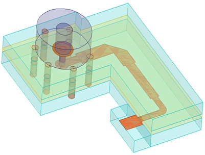
Figure 2. Simulation model of the microstrip coaxial transition.
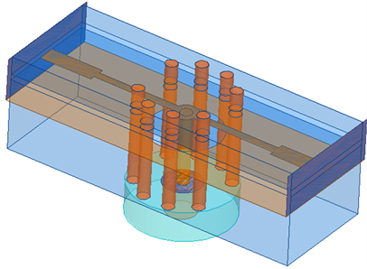
Figure 3. Simulation model of the internal divider.
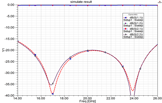
Figure 4. Simulation results of the above structure.

Figure 5. Simulation results of the internal divider.
From the simulation results we can see, in the K band, the transmission insertion loss of the vertical transition of the high frequency PCB substrate is less than 0.5 dB, and the return loss is more than 15 dB.
The multi-channel transceiver circuit and power division network is very compact, 5 layers high frequency PCB substrate is used, 1.7 mm in thickness. The top 2 layers arrangement for microwave signal; the lower 3 layers arrangement for the various data control line and the power line. Bottom layer is arranging for GND. According to the space arrangement, the form layout is shown in Figures 6-8. Among them, 1 for the multi-channel transceiver circuit module, 2 for power division network, 3 for dielectric substrate, 4 for low frequency control pad, 5 for power supply pad, 6 for RF port connected with antenna, 7 for transceiver common public port, 8 for low frequency control and power supply interface, 9 for metal isolation Cylinder, and 10 for solid grounded cylinder which conduct the thermal of the chip to the bottom of the printed board.
As shown in Figure 6, device mounting interface and power division network are in the same layer. In order to reduce the influence between circuit routing, all around use the metal isolation column to realize electromagnetic shielding. The low frequency control and the power supply of the chip are connected with pads near the chip. Below the pad there are metallized holes connected with the printed circuit board, as shown in Figure 7. At the same time, the solid grounded column designed under the chip mounting interface not only provide ground for the chip but also conduct the thermal of the chip to the bottom of the printed board, as shown in Figure 8.

Figure 6. Upper surface of integrated multilayer printed board.

Figure 7. Lower surface of integrated multilayer printed board.

Figure 8. Isolation, heat dissipation and grounding design of the integrated multilayer printed board.
4. Test Results and Analysis
Figure 9 shows the processed PCB multilayer substrate.
In order to verify the performance of integrated circuit, we design the test fixture and do the measurement, as shown in Figure 10. In the test fixture, we use the structure of fuzz button transition to ssmp.
The measurement result is shown in Figure 11 and Figure 12. From the pictures we can see that the integrated circuit working normally, the insert loss of each channel is about 16 dB from 17 GHz to 25 GHz. Deduct the loss of test fixture and adapter, the loss of each channel is about 14 dB (include 12 dB loss of power division network), the input return loss and output return loss is more than 10 dB. The channel amplitude and phase consistency are very good.

Figure 9. The high frequency PCB multilayer substrate.

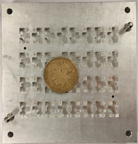
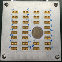

Figure 10. The tile type multi-channel transceiver module and the test fixture.

Figure 11. The Passive test results of each channel: S21 (dB) and S22 (dB).
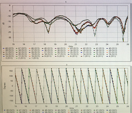
Figure 12. The Passive test results of each channel: S11 (dB) and S21 (phase).
5. Conclusion
Tile type multi-channel transceiver module using high frequency PCB technology in microwave band is proposed in this paper. High frequency PCB substrate is arranged not only for microwave transmission line, but also for low frequency control and power supply line. The use of vertical interconnection transition method realizes three-dimensional microwave signal transmission which is different from the traditional T/R module. Through the multi-layer wiring technology, the PCB substrate achieves a good microwave signal transmission. The tile type T/R module developed in this paper has the advantage of high integration, small volume and light weight, it can well satisfy the requirement of active phased array antenna in the future.
Conflicts of Interest
The authors declare no conflicts of interest regarding the publication of this paper.
Cite this paper
Tai, F.Z. and Zhang, J. (2018) Tile Type Multi-Channel Transceiver Module Applied for Phased Array Antenna. Journal of Computer and Communications, 6, 56-63. https://doi.org/10.4236/jcc.2018.612005
References
- 1. Heyen, J., von Kerssenbrock, T., Chernyakov, A., Heide, P. and Jacob, A.F. (2003) Novel LTCC/BGA Modules for Highly Integrated Millimeter-Wave Transceivers. MTT-S, 51, 2589-2596. https://doi.org/10.1109/TMTT.2003.819210
- 2. Meinel Holger, H. (1995) Commercial Applications of Millimeterwaves Present Status and Future Trends. IEEE Transactions on Microwave Theory and Techniques, 43, 1639-1653. https://doi.org/10.1109/22.392935
- 3. Lai, I.C.H. and Fujishima, M. (2008) Design and Modeling of Millimeter-Wave CMOS Circuits for Wireless Transceivers. Springer, Japan.
- 4. Gauthier, G., Bertinet, J.P. and Schroth, J. (2006) Low-Cost Ka-Band Transmitter for VSAT Applications. IEEE MTT-S International, Microwave Symposium Digest, 1398-1401. https://doi.org/10.1109/MWSYM.2006.249530
- 5. Jin, L., Loyez, C., Rolland, N., et al. (2010) An UWB Millimeter-Wave Transceiver Architecture for Wireless Sensor Networks Applications. 40th European Microwave Conference, 377-380.
- 6. Sai, W.W. and Lei, Z. (2008) Ultra-Wideband Power Divider with Good In-Band Splitting and isolation Performances. IEEE Microwave and Wireless Components Letters, 18, 518-520. https://doi.org/10.1109/LMWC.2008.2001009
- 7. Amaya, R.E., Li, M., Hettak, K., et al. (2010) A Broadband 3D Vertical Microstrip to Stripline Transition in LTCC Using a Quasi-Coaxial Structure for Millimetre-Wave SOP Applications. 40th European Microwave Conference, 109-112.