Paper Menu >>
Journal Menu >>
 Engineering, 2009, 1, 201-210 doi:10.4236/eng.2009.13024 Published Online November 2009 (http://www.scirp.org/journal/eng). Copyright © 2009 SciRes. ENGINEERING Quasi-Square Wave Mode Phase-Shifted PWM LCC Resonant Converter for Regulated Power Supply S. PADMANABHAN, Y. SUKHI, Y. JEYASHREE R M K Engineering College, Anna University, Chennai, India E-mail:sukhirmk03@gmail.com Received January 10, 2009; revised February 21, 2009; accepted February 23, 2009 Abstract This paper presents an improved self sustained oscillating controller circuit using LCC components for im- proving the overall efficiency of the system. It has a micro controller based active controller, which controls the performance from no-load up to full-load. The steady state characteristics are developed and a design example is given in detail. The proposed controller allows zero current switching at any loading condition which results in a reasonable reduction of power loss during switching with a promising efficiency. Analyti- cal and experimental results verify the achievement the design specifications. Keywords: Zero Voltage Switching, Zero Current Switching, DC-DC Converter, Resonant Converter, Soft Switching 1. Introduction With ever increasing concerns about electromagnetic compatibility (EMC) issues, more attention is being paid to resonant converters as they provide better sinusoidal waveforms. Furthermore, resonant converters can make use of natural oscillation to achieve zero voltage switch- ing (ZVS) and/or zero current switching (ZCS) thus eliminating switching losses [1]. As such both higher power-packing densities and conversion efficiencies can be achieved at high switching frequencies without snub- bers. The full-bridge converter is widely used in power dc–dc conversions because it can achieve soft-switching with the help of LCC components added in the circuit [2]. The soft-switching techniques for PWM full bridge con- verter can be classified into two kinds: one is zero-volt- age-switching (ZVS) and the other is zero-current- switching (ZCS). For dc-dc power conversion applica- tions, the conventional phase-shift full-bridge dc/dc converter has drawn more attention in recent decades due to its advantages: high conversion efficiency, high power density, and low electro magnetic interference [3–8]. In order to obtain high conversion efficiency for dc-dc power conversion applications, a soft-switched dc/dc converter with a LCC primary-side energy storage ele- ments based on [9–12] is studied and implemented in this paper. Section II presents the principle of operation of the LCC resonant converter. Successively, the Section III deal with the mathematical analysis of converter. The performance characteristics of the converter are obtained from the mathematical analysis in section IV. An optimum design procedure of this converter is proposed in section V paper only after having a study on the performance characteristics of the LCC resonant converter and it can be considered as a design reference for other engineers. Finally, a 100-kHz, 48W (40V/1.2A) laboratory-made prototype is built up to verify all the theoretical analysis and evaluation. The highest full-load conversion effi- ciency of this converter reaches about 95.56%. Com- pared with the traditional dc/dc converter, its advantage in high conversion efficiency shows good potential for various dc-dc power converter applications. Finally, some conclusions of the work are provided in Section IX. 2. Principle of Operation Like switch mode dc-to-dc converter, resonant convert- ers are used to convert dc-to-dc through an additional conversion stage: the resonant stage in which dc signal is converted to high frequency ac signal. The potential 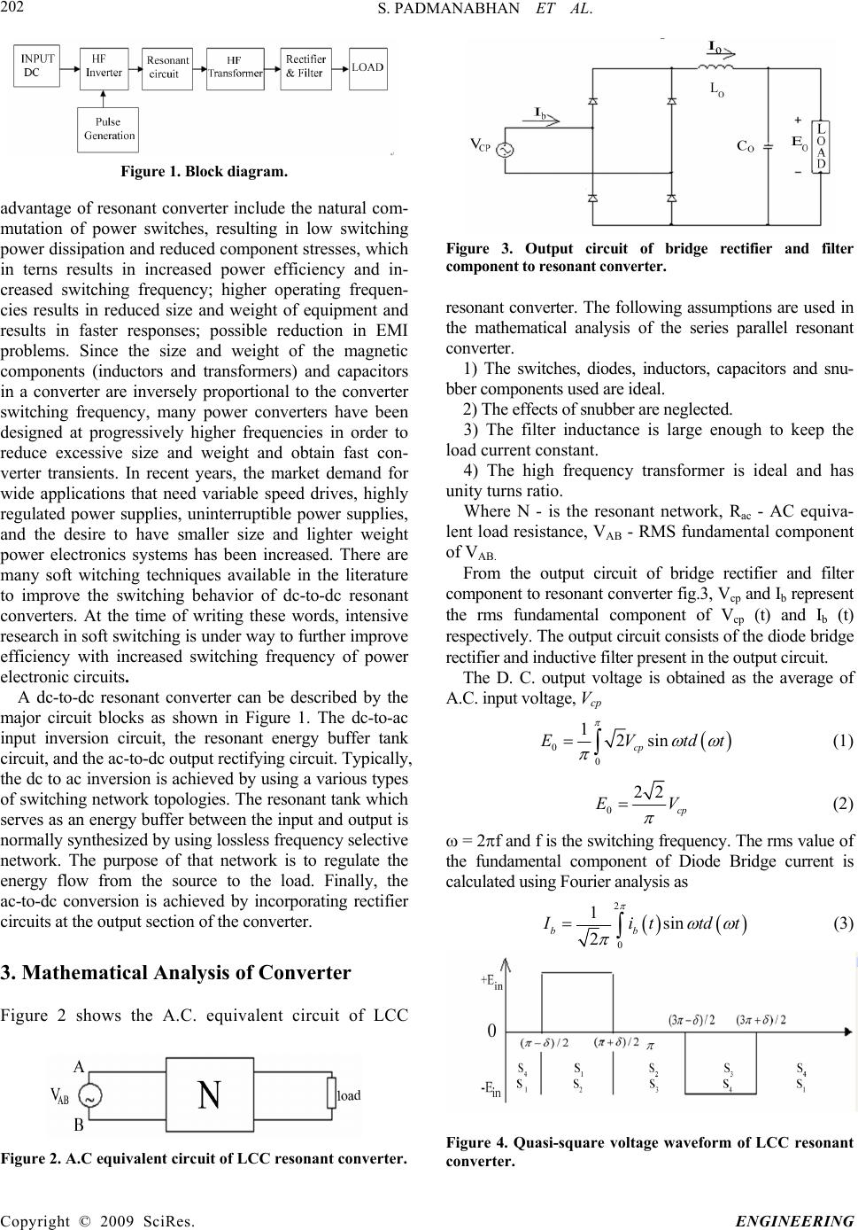 S. PADMANABHAN ET AL. Copyright © 2009 SciRes. ENGINEERING 202 Figure 1. Block diagram. advantage of resonant converter include the natural com- mutation of power switches, resulting in low switching power dissipation and reduced component stresses, which in terns results in increased power efficiency and in- creased switching frequency; higher operating frequen- cies results in reduced size and weight of equipment and results in faster responses; possible reduction in EMI problems. Since the size and weight of the magnetic components (inductors and transformers) and capacitors in a converter are inversely proportional to the converter switching frequency, many power converters have been designed at progressively higher frequencies in order to reduce excessive size and weight and obtain fast con- verter transients. In recent years, the market demand for wide applications that need variable speed drives, highly regulated power supplies, uninterruptible power supplies, and the desire to have smaller size and lighter weight power electronics systems has been increased. There are many soft witching techniques available in the literature to improve the switching behavior of dc-to-dc resonant converters. At the time of writing these words, intensive research in soft switching is under way to further improve efficiency with increased switching frequency of power electronic circuits. A dc-to-dc resonant converter can be described by the major circuit blocks as shown in Figure 1. The dc-to-ac input inversion circuit, the resonant energy buffer tank circuit, and the ac-to-dc output rectifying circuit. Typically, the dc to ac inversion is achieved by using a various types of switching network topologies. The resonant tank which serves as an energy buffer between the input and output is normally synthesized by using lossless frequency selective network. The purpose of that network is to regulate the energy flow from the source to the load. Finally, the ac-to-dc conversion is achieved by incorporating rectifier circuits at the output section of the converter. 3. Mathematical Analysis of Converter Figure 2 shows the A.C. equivalent circuit of LCC Figure 2. A.C equivalent circuit of LCC resonant converter. Figure 3. Output circuit of bridge rectifier and filter component to resonant converter. resonant converter. The following assumptions are used in the mathematical analysis of the series parallel resonant converter. 1) The switches, diodes, inductors, capacitors and snu- bber components used are ideal. 2) The effects of snubber are neglected. 3) The filter inductance is large enough to keep the load current constant. 4) The high frequency transformer is ideal and has unity turns ratio. Where N - is the resonant network, Rac - AC equiva- lent load resistance, VAB - RMS fundamental component of VAB. From the output circuit of bridge rectifier and filter component to resonant converter fig.3, Vcp and Ib represent the rms fundamental component of Vcp (t) and Ib (t) respectively. The output circuit consists of the diode bridge rectifier and inductive filter present in the output circuit. The D. C. output voltage is obtained as the average of A.C. input voltage, Vcp 0 0 12sin cp EVtd t (1) 0 22 cp E V (2) = 2f and f is the switching frequency. The rms value of the fundamental component of Diode Bridge current is calculated using Fourier analysis as 2 0 1sin 2 bb I ittd t (3) Figure 4. Quasi-square voltage waveform of LCC resonant converter. 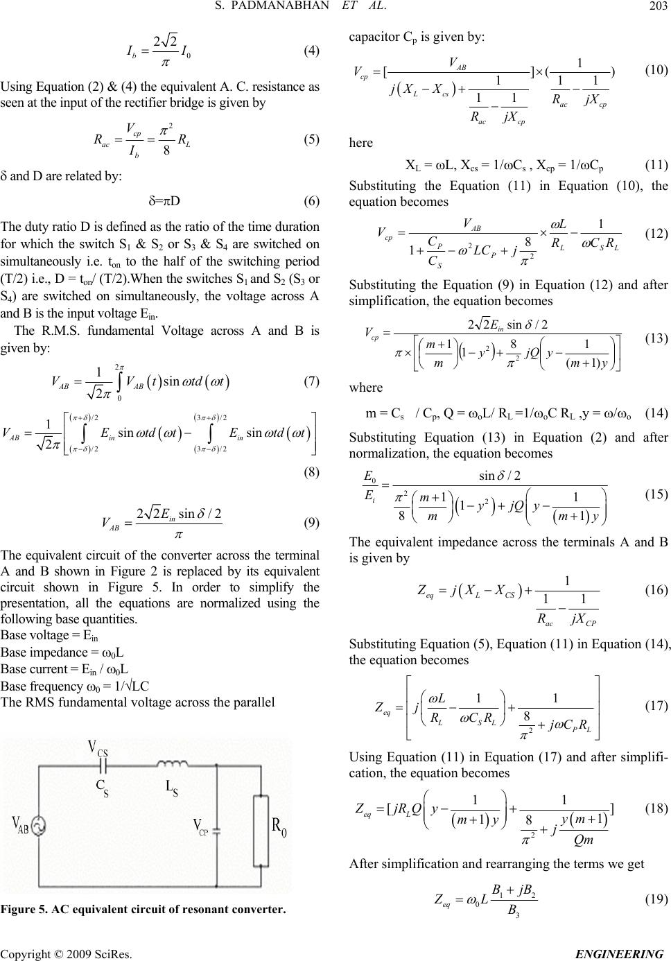 S. PADMANABHAN ET AL.203 0 22 b I I (4) Using Equation (2) & (4) the equivalent A. C. resistance as seen at the input of the rectifier bridge is given by 2 8 cp ac L b V R I R (5) and D are related by: =D (6) The duty ratio D is defined as the ratio of the time duration for which the switch S1 & S2 or S3 & S4 are switched on simultaneously i.e. ton to the half of the switching period (T/2) i.e., D = ton/ (T/2).When the switches S1 and S2 (S3 or S4) are switched on simultaneously, the voltage across A and B is the input voltage Ein. The R.M.S. fundamental Voltage across A and B is given by: 2 0 1sin 2 AB AB VVttd t (7) /23 /2 /23 /2 1sin sin 2 AB inin VEtdtEt dt (8) 22sin /2 in AB E V (9) The equivalent circuit of the converter across the terminal A and B shown in Figure 2 is replaced by its equivalent circuit shown in Figure 5. In order to simplify the presentation, all the equations are normalized using the following base quantities. Base voltage = Ein Base impedance = 0L Base current = Ein / 0L Base frequency 0 = 1/√LC The RMS fundamental voltage across the parallel Figure 5. AC equivalent circuit of resonant converter. capacitor Cp is given by: 1 []( 11 11 AB cp Lcs ac cp ac cp V V jX XRjX RjX ) 1 (10) here XL = L, Xcs = 1/Cs , Xcp = 1/Cp (11) Substituting the Equation (11) in Equation (10), the equation becomes LSL P S P AB cp RCR L jLC C C V V 1 8 12 2 (12) Substituting the Equation (9) in Equation (12) and after simplification, the equation becomes ym yjQy m m E Vin cp )1( 18 1 1 2/sin22 2 2 (13) where m = Cs / Cp, Q = oL/ RL =1/oC RL ,y = /o (14) Substituting Equation (13) in Equation (2) and after normalization, the equation becomes 0 2 2 sin/ 2 11 1 81 i E EmyjQy mm y (15) The equivalent impedance across the terminals A and B is given by 1 11 eqL CS ac CP ZjXX RjX (16) Substituting Equation (5), Equation (11) in Equation (14), the equation becomes 2 11 8 eq LSL PL L Zj RCR j CR (17) Using Equation (11) in Equation (17) and after simplifi- cation, the equation becomes 2 11 [] 1 18 eq L ZjRQy ym my jQm (18) After simplification and rearranging the terms we get 1 0 3 eq BjB ZL B 2 (19) Copyright © 2009 SciRes. ENGINEERING  S. PADMANABHAN ET AL. Copyright © 2009 SciRes. ENGINEERING 204 where 2 12 8 1 Qm Bym (20) 23 1 1( m By B ym ym 1) (21) 32 8 1(1) Qm Bym (22) Normalizing Equation (19), the equation becomes 12 3 j eqpu eqpu BjB Z Ze B (23) 22 12 2 3 eqpu BB ZB (24) Impedance angle 11 2 tan B B (25) The resonant link current I AB equ V I Z (26) II (27) where AB equ V IZ (28) Substituting Equation (9) in Equation (4) and after nor- malization, the equation becomes 22sin 2 pu equ IZ (29) Peak Inductor is given by 4sin 2 2 ppu ppu equ II Z (30) 0 cs cs ppu X VI L (31) Using (30) Peak Voltage across Cs is calculated as (1 ppu cs ppu I Vym ) (32) The peak Voltage across CP is obtained using Equation (1) and rearranging the terms. 2 O cp ppu in E VE (33) The load ripple voltage is given by, 1/2 22 accrms c VVV (34) Vcrms is the total rms load voltage.Vo is the average load voltage. The Voltage ripple factor, which is a measure of the rip- ple content, is given by the equation ac c V RF V (35) Similarly the Voltage ripple factor using the filter ele- ments is given by the equation 2rms c V RipplleFactor V (36) where V2rms represents the rms value of the second har- monic component. 22 32 m rms V VLC (37) where Vm represents the maximum value of voltage after rectification. The efficiency of the converter is calculated using the expression % out in P P 100 (38) 4. Performance Characteristics 4.1. Variation of Input Impedance Magnitude and Phase Angle vs. Normalized Switching Frequency The effect of impendence on circuit performance has been studied using Equation (19) to Equation (22) and have been used to draw the curves of the variation of the normalized input impedance magnitude and impedance phase angle, with change in normalized switching yield stress for various values of Q are shown in Figure 6 and Figure 7 respectively. It can be seen that for a particular value of quality factor Q the impedance magnitude decreases as the frequency increases up to a certain value, after which it increases with frequency, but with less effect. The effect of quality factor variation can also be observed. As Q decreases the input impedance magnitude verses normalized switching fre- quency curve shifts towards higher frequency. It is observed that at about 0.9pu frequency, all the input 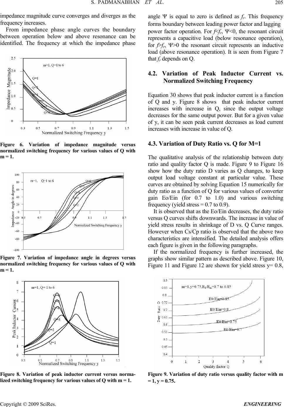 S. PADMANABHAN ET AL.205 impedance magnitude curve converges and diverges as the frequency increases. From impedance phase angle curves the boundary between operation below and above resonance can be identified. The frequency at which the impedance phase Figure 6. Variation of impedance magnitude versus normalized switching frequency for various values of Q with m = 1. Figure 7. Variation of impedance angle in degrees versus normalized switching frequency for various values of Q with m = 1. Figure 8. Variation of peak inductor current versus norma- lized switching frequency for various values of Q with m = 1. angle is equal to zero is defined as fr. This frequency forms boundary between leading power factor and lagging power factor operation. For f<fr, <0, the resonant circuit represents a capacitive load (below resonance operation), for f>fr, >0 the resonant circuit represents an inductive load (above resonance operation). It is seen from Figure 7 that fr depends on Q. 4.2. Variation of Peak Inductor Current vs. Normalized Switching Frequency Equation 30 shows that peak inductor current is a function of Q and y. Figure 8 shows that peak inductor current increases with increase in Q, since the output voltage decreases for the same output power. But for a given value of y, it can be seen peak current decreases as load current increases with increase in value of Q. 4.3. Variation of Duty Ratio vs. Q for M=1 The qualitative analysis of the relationship between duty ratio and quality factor Q is made. Figure 9 to Figure 16 show how the duty ratio D varies as Q changes, to keep output load voltage constant at particular value. These curves are obtained by solving Equation 15 numerically for duty ratio as a function of Q for various values of converter gain Eo/Ein (for 0.7 to 1.0) and various switching frequency (yield stress = 0.7 to 0.9). It is observed that as the Eo/Ein decreases, the duty ratio versus Q curves shifts downwards. The increase in value of yield stress results in shrinkage of D vs. Q Curve ranges. However when Cs/Cp ratio is observed that the above two characteristics are intensified. The detailed analysis offers each figure is given in the following paragraphs. If the normalized frequency is further increased, the graphs show similar pattern as described above. Figure 10, Figure 11 and Figure 12 are shown for yield stress y= 0.8, Figure 9. Variation of duty ratio versus quality factor with m = 1, y = 0.75. Copyright © 2009 SciRes. ENGINEERING 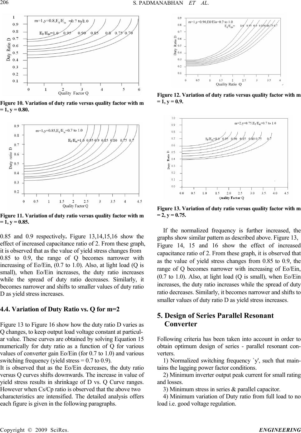 S. PADMANABHAN ET AL. Copyright © 2009 SciRes. ENGINEERING 206 Figure 10. Variation of duty ratio versus quality factor with m = 1, y = 0.80. Figure 11. Variation of duty ratio versus quality factor with m = 1, y = 0.85. 0.85 and 0.9 respectively. Figure 13,14,15,16 show the effect of increased capacitance ratio of 2. From these graph, it is observed that as the value of yield stress changes from 0.85 to 0.9, the range of Q becomes narrower with increasing of Eo/Ein, (0.7 to 1.0). Also, at light load (Q is small), when Eo/Ein increases, the duty ratio increases while the spread of duty ratio decreases. Similarly, it becomes narrower and shifts to smaller values of duty ratio D as yield stress increases. 4.4. Variation of Duty Ratio vs. Q for m=2 Figure 13 to Figure 16 show how the duty ratio D varies as Q changes, to keep output load voltage constant at particul- ar value. These curves are obtained by solving Equation 15 numerically for duty ratio as a function of Q for various values of converter gain Eo/Ein (for 0.7 to 1.0) and various switching frequency (yield stress = 0.7 to 0.9). It is observed that as the Eo/Ein decreases, the duty ratio versus Q curves shifts downwards. The increase in value of yield stress results in shrinkage of D vs. Q Curve ranges. However when Cs/Cp ratio is observed that the above two characteristics are intensified. The detailed analysis offers each figure is given in the following paragraphs. Figure 12. Variation of duty ratio versus quality factor with m = 1, y = 0.9. Figure 13. Variation of duty ratio versus quality factor with m = 2, y = 0.75. If the normalized frequency is further increased, the graphs show similar pattern as described above. Figure 13, Figure 14, 15 and 16 show the effect of increased capacitance ratio of 2. From these graph, it is observed that as the value of yield stress changes from 0.85 to 0.9, the range of Q becomes narrower with increasing of Eo/Ein, (0.7 to 1.0). Also, at light load (Q is small), when Eo/Ein increases, the duty ratio increases while the spread of duty ratio decreases. Similarly, it becomes narrower and shifts to smaller values of duty ratio D as yield stress increases. 5. Design of Series Parallel Resonant Converter Following criteria has been taken into account in order to obtain optimum design of series - parallel resonant con- verters. 1) Normalized switching frequency `y', such that main- tains the lagging power factor conditions. 2) Minimum inverter output peak current for small rating and losses. 3) Minimum stress in series & parallel capacitor. 4) Minimum variation of Duty ratio from full load to no load i.e. good voltage regulation. 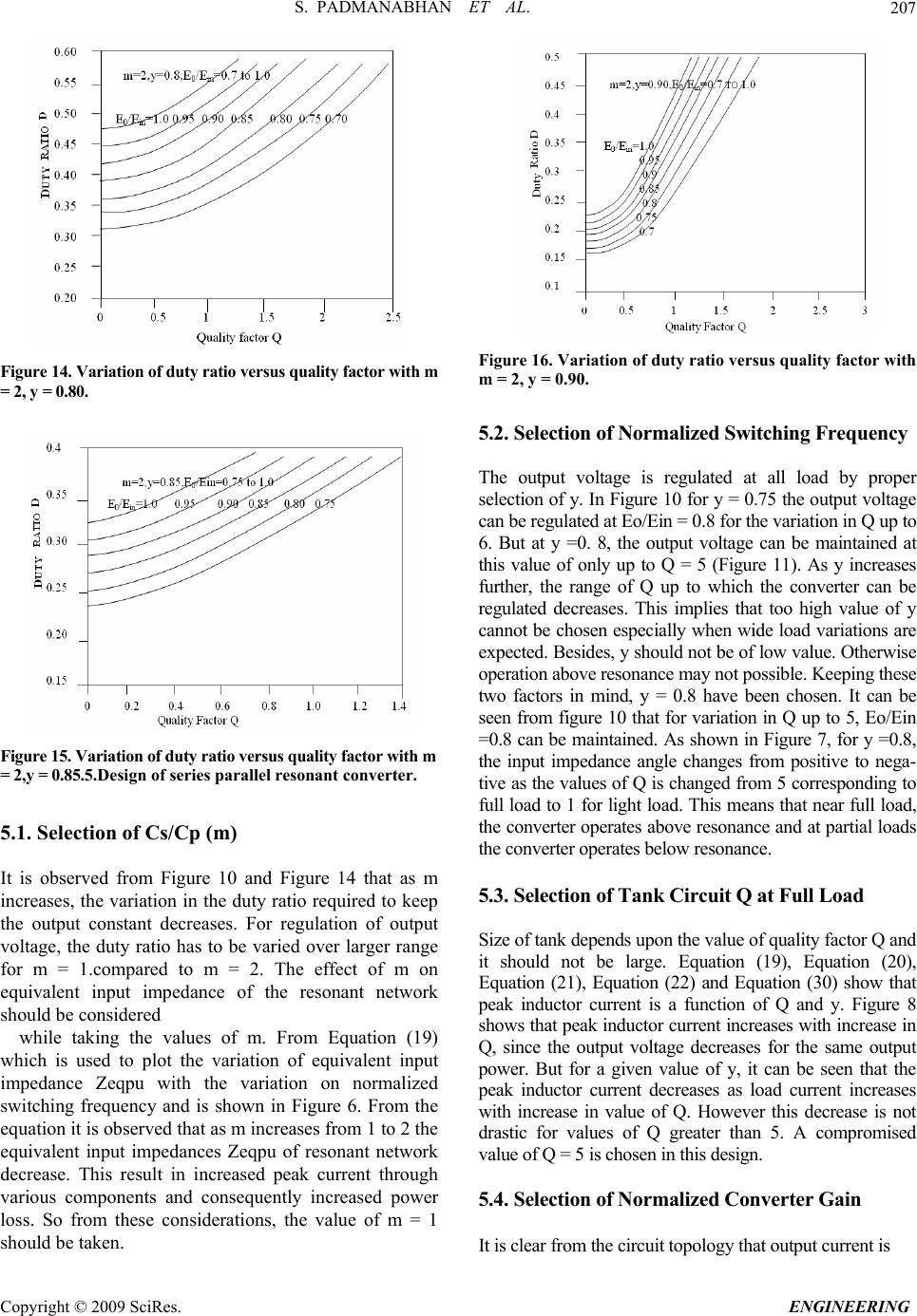 S. PADMANABHAN ET AL.207 Figure 14. Variation of duty ratio versus quality factor with m = 2, y = 0.80. Figure 15. Variation of duty ratio versus quality factor with m = 2,y = 0.85.5.Design of series parallel resonant converter. 5.1. Selection of Cs/Cp (m) It is observed from Figure 10 and Figure 14 that as m increases, the variation in the duty ratio required to keep the output constant decreases. For regulation of output voltage, the duty ratio has to be varied over larger range for m = 1.compared to m = 2. The effect of m on equivalent input impedance of the resonant network should be considered while taking the values of m. From Equation (19) which is used to plot the variation of equivalent input impedance Zeqpu with the variation on normalized switching frequency and is shown in Figure 6. From the equation it is observed that as m increases from 1 to 2 the equivalent input impedances Zeqpu of resonant network decrease. This result in increased peak current through various components and consequently increased power loss. So from these considerations, the value of m = 1 should be taken. Figure 16. Variation of duty ratio versus quality factor with m = 2, y = 0.90. 5.2. Selection of Normalized Switching Frequency The output voltage is regulated at all load by proper selection of y. In Figure 10 for y = 0.75 the output voltage can be regulated at Eo/Ein = 0.8 for the variation in Q up to 6. But at y =0. 8, the output voltage can be maintained at this value of only up to Q = 5 (Figure 11). As y increases further, the range of Q up to which the converter can be regulated decreases. This implies that too high value of y cannot be chosen especially when wide load variations are expected. Besides, y should not be of low value. Otherwise operation above resonance may not possible. Keeping these two factors in mind, y = 0.8 have been chosen. It can be seen from figure 10 that for variation in Q up to 5, Eo/Ein =0.8 can be maintained. As shown in Figure 7, for y =0.8, the input impedance angle changes from positive to nega- tive as the values of Q is changed from 5 corresponding to full load to 1 for light load. This means that near full load, the converter operates above resonance and at partial loads the converter operates below resonance. 5.3. Selection of Tank Circuit Q at Full Load Size of tank depends upon the value of quality factor Q and it should not be large. Equation (19), Equation (20), Equation (21), Equation (22) and Equation (30) show that peak inductor current is a function of Q and y. Figure 8 shows that peak inductor current increases with increase in Q, since the output voltage decreases for the same output power. But for a given value of y, it can be seen that the peak inductor current decreases as load current increases with increase in value of Q. However this decrease is not drastic for values of Q greater than 5. A compromised value of Q = 5 is chosen in this design. 5.4. Selection of Normalized Converter Gain It is clear from the circuit topology that output current is Copyright © 2009 SciRes. ENGINEERING 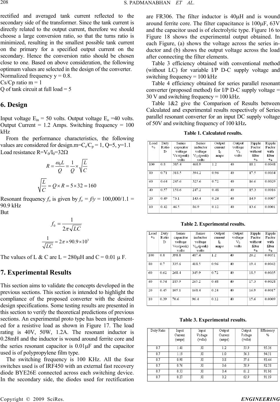 S. PADMANABHAN ET AL. Copyright © 2009 SciRes. ENGINEERING 208 rectified and averaged tank current reflected to the secondary side of the transformer. Since the tank current is directly related to the output current, therefore we should choose a large conversion ratio, so that the turns ratio is minimized, resulting in the smallest possible tank current on the primary for a specified output current on the secondary. Hence the conversion ratio should be chosen close to one. Based on above consideration, the following optimum values are selected in the design of the converter. Normalized frequency y = 0.8. Cs/Cp ratio m = 1 Q of tank circuit at full load = 5 6. Design Input voltage Ein = 50 volts. Output voltage Eo =40 volts. Output Current = 1.2 Amps. Switching frequency = 100 kHz From the performance characteristics, the following values are considered for design.m=Cs/Cp = 1, Q=5, y=1.1 Load resistance R=V0/I0=32 01 LL RQQC 5 32160 LQR C Resonant frequency fo is given by fo = f/y = 100,000/1.1 = 90.9 kHz But 0 1 2 fLC 3 1290.910 LC The values of L & C are L = 280H and C = 0.01 F. 7. Experimental Results This section aims to validate the concepts developed in the previous sections. This section is intended to highlight the compliance of the proposed converter with the desired design specifications. Some testing results are presented in this section to verify the theoretical predictions of previous sections. An experimental proto type has been implement- ed for a resistive load as shown in Figure 17. The load rating is 40V, 50W, 1.2A. The resonant inductor is 0.28mH and the inductor is wound around ferrite core and the series resonant capacitor is 0.01F and the capacitor used is of polypropylene film type. The switching frequency is 100 KHz. All the four switches used is of IRF450 with an external fast recovery diode BYE26E connected across each switching device. In the secondary side, the diodes used for rectification are FR306. The filter inductor is 40H and is wound around ferrite core. The filter capacitance is 100F, 63V and the capacitor used is of electrolytic type. Figure 16 to Figure 18 shows the experimental output obtained. In each Figure, (a) shows the voltage across the series in- ductor and (b) shows the output voltage across the load after connecting the filter elements. Table 3 efficiency obtained with conventional method (without LC) for variable I/P D-C supply voltage and switching frequency = 100 kHz Table 4 efficiency obtained for series parallel resonant converter (proposed method) for I/P D-C supply voltage = 30 V and switching frequency = 100 kHz. Table 1&2 give the Comparison of Results between Calculated and experimental results respectively of Series parallel resonant converter for an input DC supply voltage of 50V and switching frequency of 100 kHz. Table 1. Calculated results. Table 2. Experimental results. Table 3. Experimental results. 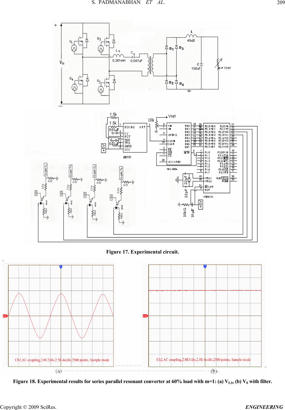 S. PADMANABHAN ET AL. Copyright © 2009 SciRes. ENGINEERING 209 Figure 17. Experimental circuit. Figure 18. Experimental results for series parallel resonant converter at 60% load with m=1: (a) VLS, (b) V0 with filter. 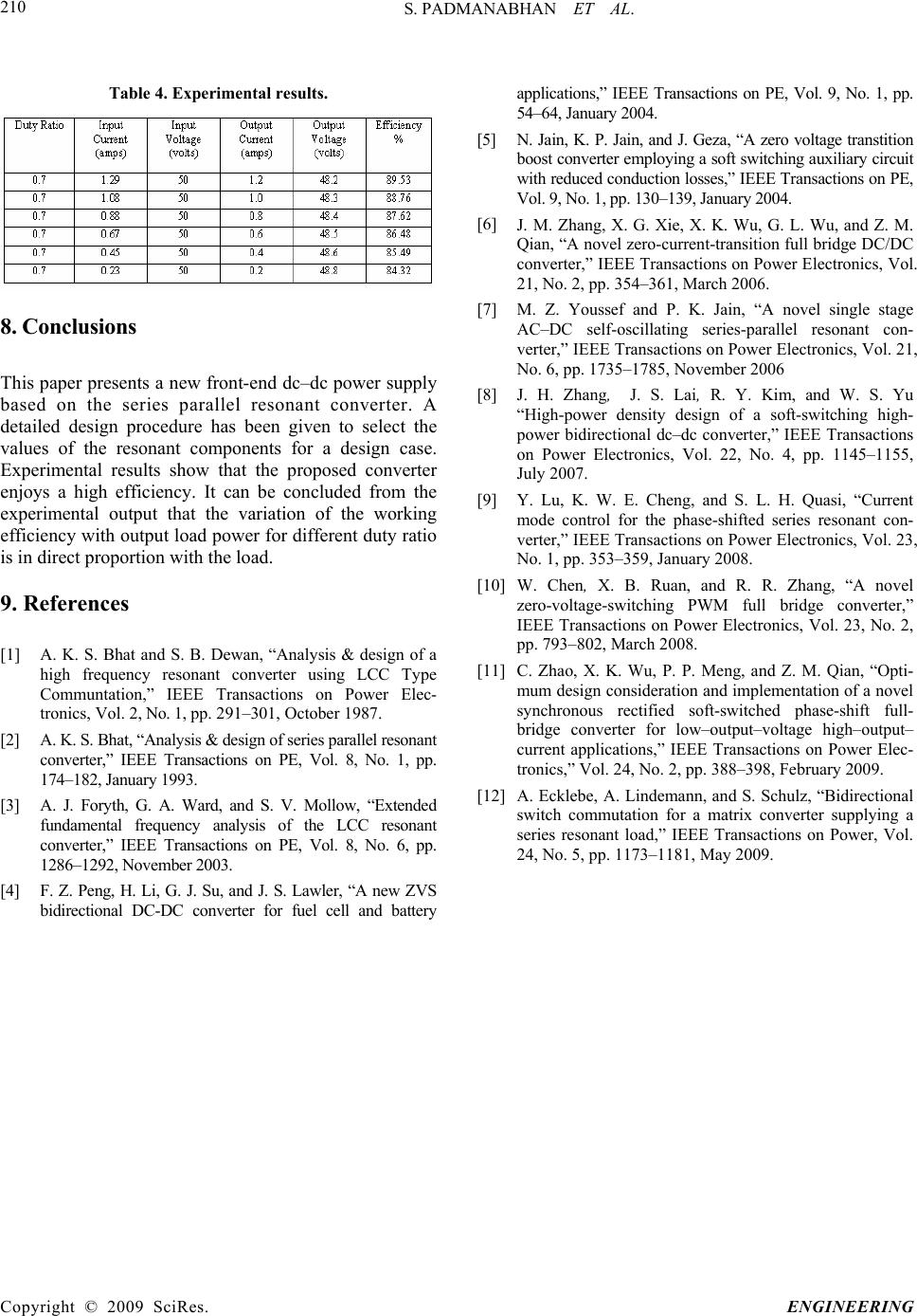 S. PADMANABHAN ET AL. Copyright © 2009 SciRes. ENGINEERING 210 Table 4. Experimental results. 8. Conclusions This paper presents a new front-end dc–dc power supply based on the series parallel resonant converter. A detailed design procedure has been given to select the values of the resonant components for a design case. Experimental results show that the proposed converter enjoys a high efficiency. It can be concluded from the experimental output that the variation of the working efficiency with output load power for different duty ratio is in direct proportion with the load. 9. References [1] A. K. S. Bhat and S. B. Dewan, “Analysis & design of a high frequency resonant converter using LCC Type Communtation,” IEEE Transactions on Power Elec- tronics, Vol. 2, No. 1, pp. 291–301, October 1987. [2] A. K. S. Bhat, “Analysis & design of series parallel resonant converter,” IEEE Transactions on PE, Vol. 8, No. 1, pp. 174–182, January 1993. [3] A. J. Foryth, G. A. Ward, and S. V. Mollow, “Extended fundamental frequency analysis of the LCC resonant converter,” IEEE Transactions on PE, Vol. 8, No. 6, pp. 1286–1292, November 2003. [4] F. Z. Peng, H. Li, G. J. Su, and J. S. Lawler, “A new ZVS bidirectional DC-DC converter for fuel cell and battery applications,” IEEE Transactions on PE, Vol. 9, No. 1, pp. 54–64, January 2004. [5] N. Jain, K. P. Jain, and J. Geza, “A zero voltage transtition boost converter employing a soft switching auxiliary circuit with reduced conduction losses,” IEEE Transactions on PE, Vol. 9, No. 1, pp. 130–139, January 2004. [6] J. M. Zhang, X. G. Xie, X. K. Wu, G. L. Wu, and Z. M. Qian, “A novel zero-current-transition full bridge DC/DC converter,” IEEE Transactions on Power Electronics, Vol. 21, No. 2, pp. 354–361, March 2006. [7] M. Z. Youssef and P. K. Jain, “A novel single stage AC–DC self-oscillating series-parallel resonant con- verter,” IEEE Transactions on Power Electronics, Vol. 21, No. 6, pp. 1735–1785, November 2006 [8] J. H. Zhang, J. S. Lai, R. Y. Kim, and W. S. Yu “High-power density design of a soft-switching high- power bidirectional dc–dc converter,” IEEE Transactions on Power Electronics, Vol. 22, No. 4, pp. 1145–1155, July 2007. [9] Y. Lu, K. W. E. Cheng, and S. L. H. Quasi, “Current mode control for the phase-shifted series resonant con- verter,” IEEE Transactions on Power Electronics, Vol. 23, No. 1, pp. 353–359, January 2008. [10] W. Chen, X. B. Ruan, and R. R. Zhang, “A novel zero-voltage-switching PWM full bridge converter,” IEEE Transactions on Power Electronics, Vol. 23, No. 2, pp. 793–802, March 2008. [11] C. Zhao, X. K. Wu, P. P. Meng, and Z. M. Qian, “Opti- mum design consideration and implementation of a novel synchronous rectified soft-switched phase-shift full- bridge converter for low–output–voltage high–output– current applications,” IEEE Transactions on Power Elec- tronics,” Vol. 24, No. 2, pp. 388–398, February 2009. [12] A. Ecklebe, A. Lindemann, and S. Schulz, “Bidirectional switch commutation for a matrix converter supplying a series resonant load,” IEEE Transactions on Power, Vol. 24, No. 5, pp. 1173–1181, May 2009. |

