Open Access Library Journal
Vol.05 No.06(2018), Article ID:85675,13 pages
10.4236/oalib.1104682
Simulation Analysis of DC-DC Circuit Based on Simulink in Intelligent Vehicle Terminal
Weiran Li, Guoping Yang
College of Automotive Engineering, Shanghai University of Engineering Science, Shanghai, China

Copyright © 2018 by authors and Open Access Library Inc.
This work is licensed under the Creative Commons Attribution International License (CC BY 4.0).
http://creativecommons.org/licenses/by/4.0/


Received: May 25, 2018; Accepted: June 26, 2018; Published: June 29, 2018
ABSTRACT
With the popularization of intelligent transportation systems, intelligent vehicle terminal has emerged. As the most important part of the Intelligent Transportation System (ITS), the smart vehicle-mounted terminal integrates technologies such as the Internet of Things, satellite navigation technology, and even artificial intelligence, and is now widely used in various modes of transportation. The output voltage of automotive vehicle power supplies is generally 12 V, 24 V, 36 V, while the operating voltage of embedded chips inside vehicle-mounted terminals such as automobiles or buses generally needs to be depressurized before they can work normally. Therefore, this paper will analyze four basic DC chopper circuits, analyze its working principle, and build a DC-DC circuit model according to Matlab/Simulink software and finally analyze the waveform of the simulation output.
Subject Areas:
Mechanical Engineering
Keywords:
Intelligent Vehicle Terminal, DC-DC, Matlab/Simulink

1. Introduction
With the development of power electronics technology, DC-DC technology has been widely used in the industrial fields of computers, communications, automobiles and aerospace. All cars are powered by DC power supplies. The various electronic components in the car also use DC power. This is bound to be applied to DC-DC technology to meet the operating voltage requirements of various automotive electronic components. This paper analyzes the working principle of four DC-DC technologies, which are DC buck chopper circuit, DC boost chopper circuit, Buck-Boost chopper circuit and Cuk chopper circuit. Finally, DC-DC circuit model will be built based on Matlab/Simulink software, and the waveform of the simulation output will be analyzed [1] .
2. Buck Chopper Circuit
2.1. The Principle of Buck Chopper Circuit
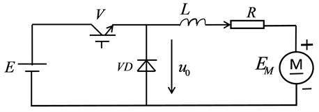
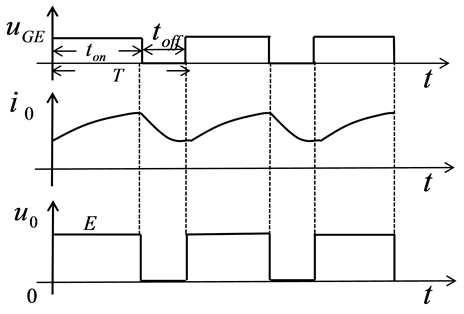
At time t = 0, the V driver is turned on and the VD is subjected to back pressure and turned off. The power supply E supplies power to the load, the load voltage U0 = E, and the load current i0 rises in an exponential manner (Figure 1).
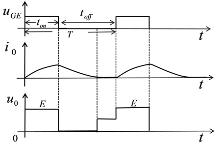
At t = t1, V is turned off and the diode VD is freewheeling. The load voltage U0 is approximately zero, and the load current decreases exponentially (Figure 2, Figure 3). The large inductor L is usually connected in series so that the load current is continuous and the ripple is small [2] .
2.2. Basic Calculation Relations
When the current is continuous, the average load voltage is:
(2-1)
α―Duty Ratio.
The maximum value of U0 is E, and if α is reduced, U0 will decrease with it reducing the chopper circuit, also known as the Buck converter.
The average load current is:
(2-2)
When the current is interrupted, the average value of U0 will be raised and it is generally undesirable [2] .
3. Boost Chopper Circuit
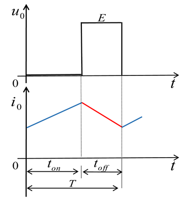
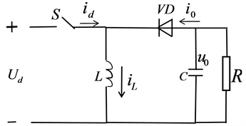
Assume that L and C are very large. When the switch is turned on, current flows through the inductor and the switch, the diode is reverse biased, and the output is isolated from the input. The power supply charges the inductor L. At this time, the diode VD between R and L is reverse biased. Due to the constant current of the inductor L, the charging current is basically a constant value iL. When VD is turned off, C is discharged to the load RL. Since C is charged and the C capacity is large, the load voltage is maintained at a constant value, and the capacitor C is directed to the load. Power supply, the output voltage U0 is constant. When the switch is turned off, the polarity of the potential changes, VD turns to positive bias, the induced potential of the inductor turns on the diode, the inductor current iL forms a loop through the diode and the load, and the inductor L superposes with the power supply to charge the capacitor C together [3] (Figures 4-7).
Figure 1. The principle diagram of the circuit.
Figure 2. The current continues.
Figure 3. The current interrupts.
Figure 4. The principle diagram of the circuit.
4. Boost and Buck Chopper Circuit
4.1. The Principle of Buck Chopper Circuit
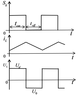
Assume that the L value is large and the C value is also large (Figure 8). The
Figure 5. Voltage and current Waveform.
Figure 6. Continuous current.
Figure 7. Insufficient current.
inductor current i1 and the capacitor voltage, i.e., the load voltage U0, are basically constant. There are two modes [3] :
Figure 8. Boost and Buck chopper circuit and its waveform.
1) When S is on, the power supply U supplies power to the L via S, and the current is i1. At the same time, C maintains the output voltage constant and supplies power to the load R.
2) When S is off, the energy of L is released to the load, and the current is i2. The polarity of the load voltage is positive and negative, and the polarity of the power supply voltage is reversed. This circuit is also referred to as a reverse polarity chopper circuit.
4.2. Basic Calculation Relations
In steady state, the integral of the voltage UL in a period T is zero:
(4-1)
When V is in the on state, UL = E; and when S is in the off state, UL = −U0. then:
(4-2)
Output voltage:
(4-3)
By changing α, the output voltage can be either higher than the supply voltage or lower than the supply voltage. When 0 < α < 1/2, the output voltage is lower than the supply voltage, and when 1/2 < α < 1, the output voltage is higher than the supply voltage. Therefore, it is called a buck-boost chopper circuit or a buck-boost converter [2] .
5. Cuk Chopper Circuit
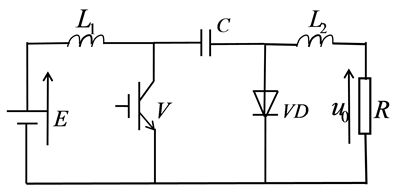
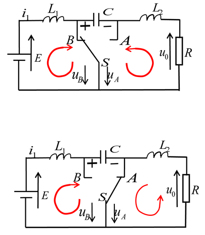
5.1. The Principle of Cuk Chopper Circuit (Figure 9, Figure 10)
Figure 9. The principle diagram of the circuit.
Figure 10. Equivalent circuit.
5.2. Basic Calculation Relations
In the steady state, the integral of the current of the capacitor C in one cycle T is zero, that is:
(5-1)
In the equivalent circuit, the time for the S point to connect to the B point is ton, So the product of capacitance current and time is I2 * ton. The time for S to connect A point is toff, so the product of capacitance current and time is I1 * toff. As a result, it can be obtained:
(5-2)
When the capacitance C is very strong, the capacitance voltage UC pulsation is sufficiently small, and the relationship between the output voltage U0 and the input voltage E can be calculated as follows [4] :
When the S point is connected to B point, B point voltage UB = 0, A point voltage UA = −UC;
When the S point is connected to A point, UB = UC, UA = 0.
Therefore, the average value of UB is [3] :
(5-3)
(5-4)
In addition, the average voltage of the voltage of the A point is:
(5-5)
(5-6)
Then we can get the relationship between the output voltage U0 and the power supply voltage E:
(5-7)
6. Simulink Circuit Simulation Analysis
According to the above principle, the simulation models are established by using the power electronic module library in MATLAB/SIMULINK software, and the corresponding parameter is set to simulate the waveform diagram.
6.1. Buck Chopper Circuit Simulation
Parameter settings:
Cycle: 0.0005 s; Duty cycle: 20%, 50%; Duration: 0.005 s; Supply voltage VDc: 12 V; Inductance L: 0.00045H; Load resistance R: 1 Ω; Capacitance C: 0.0026F; Algorithm: ode45.
The simulation diagram of the buck chopper circuit is shown in Figures 11-13 respectively represent the simulation waveforms with duty cycles of 20% and 50%. The waveforms in Figure 12 and Figure 13 are represented from top to bottom as follows: pulse waveform, load voltage UR, inductor voltage UL, inductor current IL, thyristor current, and supply current. By analyzing the waveform diagram, it can be seen that the simulation waveform is consistent with the theoretical analysis [5] .
6.2. Boost Chopper Circuit Simulation
Parameter settings:
Cycle: 0.001 s; Duty cycle: 20%, 50%; Duration: 0.01 s; Supply voltage VDc: 12 V; Inductance L: 0.001H; Load resistance R: 1 Ω; Capacitance C: 0.0026F; Algorithm: ode 23.
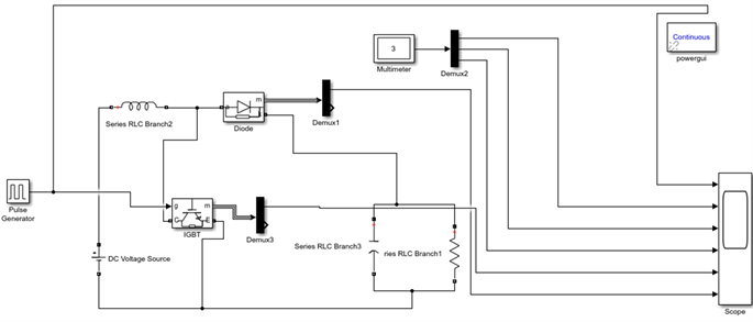
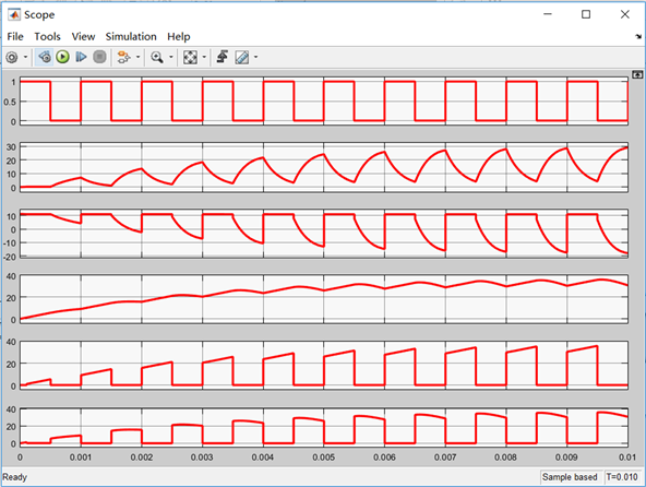
The simulation diagram of the boost chopper circuit is shown in Figure 11-13 respectively represent the simulation waveforms with duty cycles of 20% and 50%. The waveforms in Figures 14-16 are represented from top to bottom as follows: pulse waveform, load voltage UR, inductor voltage UL, inductor current
Figure 11. Buck chopper circuit simulation.
Figure 12. Duty cycle 20%.
Figure 13. Duty cycle 50%.
Figure 14. Boost chopper circuit simulation.
Figure 15. Duty cycle 20%.
Figure 16. Duty cycle 50%.
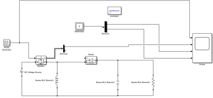
Figure 17. Boost and Buckchopper circuit simulation.
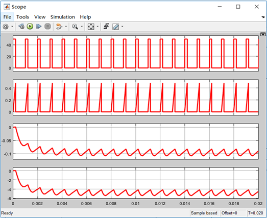
Figure 18. Duty cycle 20%.
Figure 19. Duty cycle 80%.
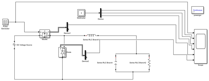
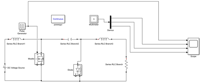
Figure 20. Cuk chopper circuit simulation.
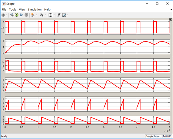
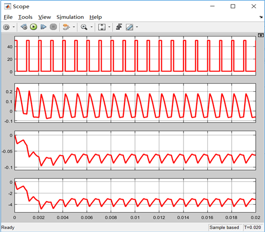
Figure 21. Duty cycle 20%.
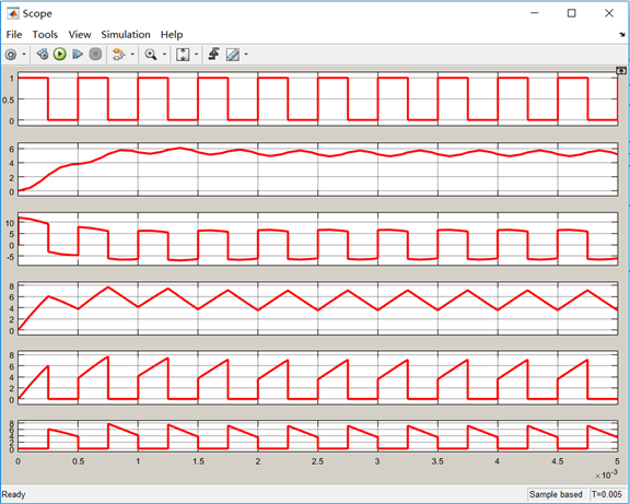
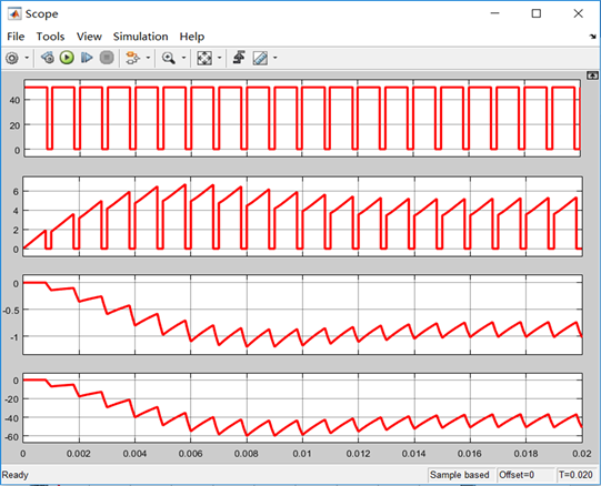
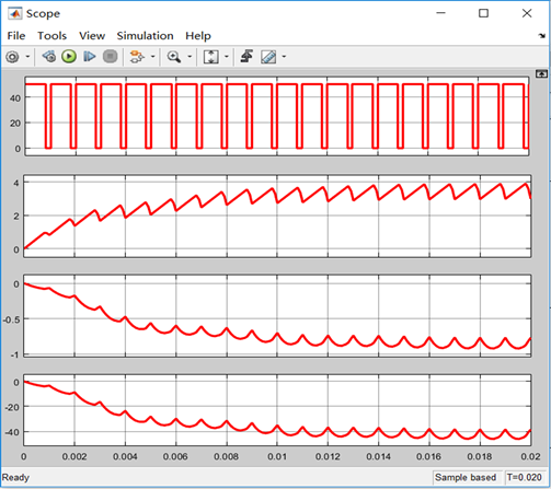
Figure 22. Duty cycle 80%.
IL, thyristor current, and supply current. By analyzing the waveform diagram, it can be seen that the simulation waveform is consistent with the theoretical analysis.
6.3. Boost and Buck Chopper Circuit
Parameter settings:
Cycle: 0.001 s; Duty cycle: 20%, 80%; Duration: 0.02 s; Supply voltage VDc: 12V; Inductance L: 5e−3; Load resistance R: 50 Ω; Capacitance C: 5e−5; Algorithm: ode45.
The simulation diagram of the boost and buck chopper circuit is shown in Figures 17-19 respectively represent the simulation waveforms with duty cycles of 20% and 80%. The waveforms in Figure 18 and Figure 19 are represented from top to bottom as follows: pulse waveform, input current, output current, output voltage. By analyzing the waveform diagram, it can be seen that the simulation waveform is consistent with the theoretical analysis.
6.4. Cuk Chopper Circuit (Figure 20)
Parameter settings:
Cycle: 0.001 s; Duty cycle: 20%, 80%; Duration: 0.02 s; Supply voltage VDc: 12V; Inductance L: 0.08H; Load resistance R: 50 Ω; Capacitance C: 1e−5; Algorithm: ode45.
The simulation diagram of the Cuk chopper circuit is shown in Figures 20-22 respectively represent the simulation waveforms with duty cycles of 20% and 80%. The waveforms in Figures 20-22 are represented from top to bottom as follows: pulse waveform, input current, output current, output voltage. By analyzing the waveform diagram, it can be seen that the simulation waveform is consistent with the theoretical analysis.
7. Conclusion
In this paper, the working principles of Buck chopper circuit, Boost chopper circuit, Buck and Boost chopper circuit, Cuk chopper circuit are analyzed, and the Matlab/Simulink software is used to set up the DC chopper circuit model. The results show that the simulation waveform is consistent with the results obtained by the conventional analysis method, and the four DC chopper circuits can well accomplish the boost and decompression. Through the simulation of these four kinds of circuits, we can see that these circuits can effectively and steadily step down the 12V DC power supply, and ultimately provide power for various electrical components in the vehicle terminal.
Cite this paper
Li, W.R. and Yang, G.P. (2018) Simulation Analysis of DC-DC Circuit Based on Simulink in Intelligent Vehicle Terminal. Open Access Library Journal, 5: e4682. https://doi.org/10.4236/oalib.1104682
References
- 1. Wei, L.M. and Lu, X.Y. (2016) A Study on DC Chopping Circuits Based on MATLAB. Journal of Jilin Engineering Normal University, No. 3, 87-89.
- 2. Li, Y.Y., Wang, Y.J. and Zhang, L.P. (2014) Modern Power Electronics Technology. 4th Edition, Tsinghua University Press, Beijing.
- 3. Wang, Y.L. (2013) Modern Power Electronics. 3th Edition, Electronic Industry Press, Beijing.
- 4. Zhao, L.B. (2006) Modern Electronic Power Base. 3th Edition, Tsinghua University Press, Beijing.
- 5. Chen, B.S. (2005) Electric Drive Automatic Control System, Motion Control System. 3th Edition, Machinery Industry Press, Beijing.


