 Materials Science s a nd Applications, 2011, 2, 1601-1621 doi:10.4236/msa.2011.211214 Published Online November 2011 (http://www.SciRP.org/journal/msa) Copyright © 2011 SciRes. MSA 1601 Predictive Modelling of Etching Process of Machinable Glass Ceramics, Boron Nitride, and Silicon Carbide Huey Tze Ting1, Kha led A bou -El- Hos se in 2, Han Bing Chua3 1School of Engineering & Science, Curtin University of Technology, Sarawak, Malaysia; 2School of Engineering, Nelson Mandela Metropolitan University, Port Elizabeth, South Africa; 3School of Engineering & Science, Curtin University of Technology, Sarawak, Malaysia. Email: ting.huey.tze@stud.curtin.edu.my, khaled.abou-el-hossein@nmmu.ac.za, chua.han.bing@curtin.edu.my Received M ay 28 th, 2011 ; revised July 30th, 2011; accept ed October 24th, 2011. ABSTRACT The present paper discusses the development of the first and second order model for predicting the chemical etching variables, namely, etching rate, surface roughness and accuracy of advanced ceramics. The first and second order etching rate, surface roughness and accuracy equations were developed using the Response Surface Method (RSM). The etching variables included etching temperature, etching duration, solution and solution concentration. The predic- tive models’ analyses were supported with the aid of the statistical software package—Design Expert (DE 7). The ef- fects of the individual etching variables and interaction between these variables were also investigated. The study showed that predictive models successfully predicted the etching rate, surface roughness and accuracy readings re- corded experimentally with 95% confident interval. The results obtained from the predictive models were also com- pared with Multilayer Perceptron Artificial Neural Network (ANN). Chemical Etching variables predictive by ANN were in good agreement with those with those obtained by RSM. This observation indicated the potential of ANN in predicting chemical etching variables thus eliminating the need for exhaustive chemical etching in optimization. Keywords: Chemical Etching, Machinable Glass Ceramic, Boron Nitride, Silicon Carbid e , RSM, ANN 1. Introduction Advanced ceramic is categorized into oxides, non-oxides and composite ceramics. It possesses great mechanical properties, such as the capability to operate under high temperature, high abrasion resistance, longer service life and dimensional stability. Their versatility has been de- monstrated in the development of aerospace and refract- tory materials, and electrical, thermal, structural and me- dical application [1]. Among advanced ceramics, machinable glass ceramics (MGC) is one of the common materials in the industry. MGC is polycrystalline material, produced with con- trolled nucleation and crystallization. These materials are unique because of their ability to be machined to precise tolerances with a good surface finish. MGC possesses low thermal conductivity and is highly recommended as high temperature insulators. It shows excellent properties, especially in semiconductor and electronics industries. MGC is white in colour and it can be highly polished without da maging its prope rties. This makes MGC a use- ful in the manufacture of medical and optical devices [2,3]. Silicon Carbide (SiC) is the most attractive mate- rial in manufacturing devices used in high power and high temperature applications. This arises from its high thermal conductivity, high electric field breakdown volt- age, and wide bandgap. SiC is also known as one of the hardest materials among advanced ceramics and it is widely used for tribological applications in extreme con- ditions because of its unique properties, such as high hardness, good corrosive resistance, and excellent che- mical stability [4]. Another MGC material is boron ni- tride (BN). BN consists of equal numbers of boron and nitrogen atoms. B is isoelectrionic to similarly structured carbon lattice and thus exists in various crystalline forms. Its hardness is inferior only to diamond, but its thermal and chemical stability is superior. Because of its excel- lent thermal and chemica l stability, BN i s widely used in the building o f high-temperature equi pment.  Predictive Modelling of Etching Process of Machinable Glass Ceramics, Boron Nitride, and Silicon Carbide 1602 Chemical etching (CHM) is the oldest non-traditional machining method of removing selected surface areas by immersing the work piece material into a chemical re- agent. The removal process will continuously take place even though the penetration rate of etching rate may be very small and over-etching might happen during the process. CHM was applied in 2500 B.C. to produce jew- elry out of copper in the citric acid and replaced hand- tool engraving process [5-7]. The development of CHM has rapidly progressed after the Second World War when North American Aviation started running mass produc- tion using CHM on rocket materials. In the 20th century, CHM was employed as a key process in the fabrication of integrated circuits, bioMEMS, and microfluidid de- vices [8-10]. CHM is well-known for its efficiency in lightening surface weight, fabrication and the production of dimensionally precise components [5,11]. In terms of cost efficiency, CHM is economically acceptable among other machining operations. With the minimum set up procedure and equipment, CHM can be carried out easily. On the other hand, CHM must be conducted in fume hood or a place that is totally covered due to the usage of chemical reagents and their hazardous effect towards human health. The disposal of waste chemical reagents is another problem encountered if CHM is chosen. How- ever, CHM requires only a short necessary machining time, hence resulting in low cost production and causing no damage on mechanical properties. Mask patterning is the most common method of fab- riccation in CHM. Yet, this method is usually accompa- nied with a few problems such as undercutting, mask adhesive issues and their unstable resistivity to chemical reagents. Thus, a new technology that is based on em- ploying CHM after indentation has been introduced. This technique has demonstrated its versatility and lower production cost using basic facilities and manufacture, simplicity of process with no material selectivity required [12]. One of the key issues of this technology is its abil- ity to increase and control the etching rate difference between indented and non-indented areas. Saito et al [13,14] were the first to develop this technique and prove its feasibility for micro-machining and fabrication of alumina-silicate glass. Nagai et al. [15] and Kang and Youn [12] who fabricated micro-patterns on advanced ceramics, found in this technique a substitute for the ap- plication of masks. Various studies have been reported on the machining operations of advanced ceramics [16-24] such as deep reactive-ion etching [25], powder blasting [26-28], laser drilling [29-31], and conventional machining [32-34]. In terms of the etching process, chemical etching is among the most commonly used method compared to other ad- vanced machining methods (laser beam machining, elec- tron discharge machining and etch). Watanabe [35] ob- tained a linear relationship between etching rate and temperature while comparing wet etching and mechanic- cal machining. Willia ms et al. [36] stated that not all ma- terials were etched in all etchants due to time limitations. This is probably caused by the limited chemical reaction. Gaiseanu et al. [37] found that relationship between etching duration and etching rate was significant in in- fluencing the HF etching results of boron nitride. Minhao et al. [38] performed their etching experiments on silicon at a constant etching period and reported that the etching rate obtained was surprisingly linear. They concluded that a mino r cha nge of e tchi ng time had sl ightl y cha nged the linear shape of etching rate to curvature. Olsen et al. [39] also indicated that an increased in etching time would decrease the bond strengths of alumino silicate in HCl etching. The present study will provide some important scien- tific findings on CHM of advanced ceramics with solu- tion of HCl, HBr and H3PO4. T his paper will also discuss on various types of DoE and its application, identify ma- terial machinability and highlight the relationship be- tween etching rates, surface roughness and dimensional accuracy, and present the predictive models by RSM and ANN. 2. Design of Experiment (DoE) In manufacturing processes, a few practical problems related to the process parameters that determine the de- sired product quality, optimization and maximizing of manufacturing system performance often occur. In order to attain a high quality process with suitable variables, different statistical methodologies have been proposed to simulate the various conditions encountered during ma- terial processing and establish relationship between pa- rameters and variables for a better system understanding and control. By selecting a suitable experimental design method, it is able to reduce the necessary number of ex- perimental runs and filter out effects due to statistical variations. A number of experimental design methods have been developed for experimental planning and data acquisition. The Design of Experimental (DoE) is well- known in data analysis, process optimization and charac- terization of complicated processes. With a relatively small number of experimental runs, DoE is able to rea- sonably establish the relationship between etching pa- rameters and process performance. Many researchers have design their experiment through DoE to filter out the secondary factors. DoE is combination of mathematical and statistical techniques used to predict and analyze process behavior in different conditions with relatively fewer, but essential number of experiment tests [40]. The technique is cate- Copyright © 2011 SciRes. MSA  Predictive Modelling of Etching Process of Machinable Glass Ceramics, Boron Nitride, and Silicon Carbide Copyright © 2011 SciRes. MSA 1603 gorized by the number and level of variables, objective and characteristics of processing. Basically, there are similar designs, where the statistical method is applied in the ana lysis with ANOV A and o ther releva nt infor ma - tion [40-42]. Table 1 shows the design se lection of DoE. Response surface objective is used to perform optimiza- tion of the processes, to troubleshoot problems and to make processes more robust against external and non- controllable influences. Many research studies have shown that DoE approach was able to eliminate secondary factors by reducing the effect of the process period [42,43]. Pierlot et al. [44] indicated the ability of DoE to determine the influences of process variables on the responses and to estimate the significance of the regression equation coefficients. They also indicated the advantage of DoE in increasing the data accuracy by filtering out the errors from the process. Subramanian et al. [45] reported that DoE significantly improved the etching result of niobium cavities by re- ducing the number of testing and successfully reduced thee parameter range. Chen et al. [46] applied the DoE method to optimize etching process in commercial etch- ers and the optimization result was in good agreement with the experimental data. 2.1. 2k Factorial Design The factorial design allows each complete test or rep- lication of all the possible combinations of the levels of the factors to be investigated. The 2k factorial design is a screening method, a linear process and first level model. By applying this method, each of the results is pre- ex- amined and the range of the variables is determined. The specialty of 2k factorial design is that its ANOVA con- sists of a curvature term, which is used to the nature of the process. If the curvature term is signifycant, the cor- responding process will have t o proceed to the ne xt stage (second order model). In contrast, the corresponding re- sult will proceed to the first order model analysis. This is because a significant curvature in ANOVA indicates the relationship between variables exists and a higher level of model should be used to study the related process, as the 2k factorial design only capable of studying linear process. As a screening method, graphs produced by 2k facto- rial design are used to determine the range of variables. If the line positively increases, it means that the variables’ range might fall at a higher level, and vice versa. The advantages of this method are that it is able to reduce the number of experimental runs, the process period and in- crease the cost effectiveness. Usi ng the 2 k factorial design of experiment, a mathematical model (first-order) of etch- ing rate, surface roughness and dimensional accuracy as a function of etching temperature, etching duration, etch- ing solution and solution concentration has been devel- oped with a 95% confidence level. These model equations have been used to develop contours of each result [47]. 2.2. Response Surface Methodology (RSM) RSM is a statistical tool used to analyse complicated processes in which h a response of interest is influenced by several factor [41]. The Central Composite design (CCD), Box-Behnken design and 33 design are the most common RSM design methods. Each of these is used in different circumstances. CCD is mainly used in sequen- tial experimentation, thus making it flexible for industria l process development. It is widely used because of its ability to be partitioned naturally into two subsets: the first subset is used to estimate linear and two-factor in- teraction effects; and, second, to estimate the curvature effects of the process. Compared with other RSM designs, CCD is more efficie nt and able to pro vide more informa- tion with minimum number of experimental runs. As mentioned previously, the range of each parameter has been reduced through 2k factorial design. The pur- pose of doing this is to reduce the time taken in deter- mining the interaction of parameters and their relation- ship. In this research, the input are etching temperature, etching solution, etching duration, and etching concen- tration. Their range is stated in Table 2 and a central point is added to the process to determine the peak point for each result. This is the purpose of employing CCD as the statistical method in studying this pro cess. With three numeric factors, one categoric factor and five central points are added to DE7, the CCD is able to randomly generate 40 experimental runs for the three set of results. This is to minimize experimental errors ( such as change of temperature during experiment) and to ensure consis- tency in the result. Similar to other RSM method, p-value is the main co nsideration used in selectin g the model and determining the significant variable. Table 1. The design selection gui deli ne [40]. Number of factors Comparati v e O bjec tive Screening Objective Response Surface Objective 1 1 factor completely randomized design- - 2 - 4 Randomized block design Full/Fractional factorial Central composite/Box-Behnken 5 or more Randomized block design Fractional factorial/Plackett-BurmanScreen first to reduce number of factors 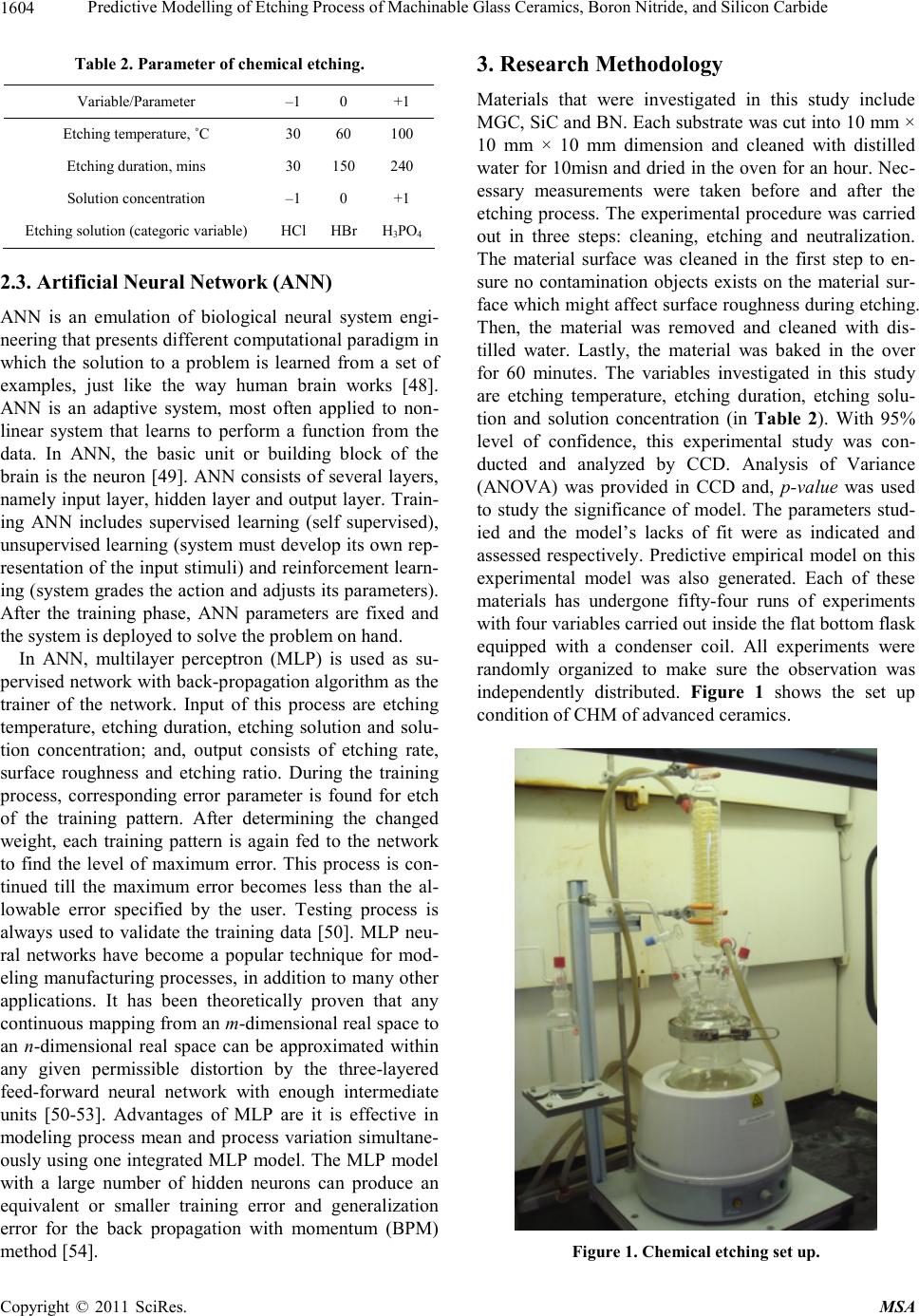 Predictive Modelling of Etching Process of Machinable Glass Ceramics, Boron Nitride, and Silicon Carbide 1604 Table 2. Parameter of chemical etching. Variable/Parameter –1 0 +1 Etching temperature, ˚C 30 60 100 Etchi ng dura tion, mins 30 150 240 Sol utio n conce ntr a tion –1 0 +1 Etching solution (categoric variab le) HCl HBr H3PO4 2.3. Artificial Neural Network (ANN) ANN is an emulation of biological neural system engi- neering that presents different computational paradigm in which the solution to a problem is learned from a set of examples, just like the way human brain works [48]. ANN is an adaptive system, most often applied to non- linear system that learns to perform a function from the data. In ANN, the basic unit or building block of the brain is the neuron [49]. ANN consists of several la yers, name ly input la yer, hid den la yer and output la yer. T rain- ing ANN includes supervised learning (self supervised), unsupervised learning (system must develop its own rep- resentation of the input stimuli) and reinforcement learn- ing (system grades the action and adjusts its parameters). After the training phase, ANN parameters are fixed and the system is deployed to solve the problem on hand. In ANN, multilayer perceptron (MLP) is used as su- per vised ne twor k with b ack-p ro pagati on algo rithm a s the trainer of the network. Input of this process are etching temperature, etching duration, etching solution and solu- tion concentration; and, output consists of etching rate, surface roughness and etching ratio. During the training process, corresponding error parameter is found for etch of the training pattern. After determining the changed weight, each training pattern is again fed to the network to find the level of maximum error. This process is con- tinued till the maximum error becomes less than the al- lowable error specified by the user. Testing process is always used to validate the training data [50]. MLP neu- ral networks have become a popular technique for mod- eling manufacturing processes , in addition to many other applications. It has been theoretically proven that any continuous mapping from an m-dimensional real space to an n-dimensional real space can be approximated within any given permissible distortion by the three-layered feed-forward neural network with enough intermediate units [50-53]. Advantages of MLP are it is effective in modeling process mean and process variation simultane- ously using one integrated MLP model. The MLP model with a large number of hidden neurons can produce an equivalent or smaller training error and generalization error for the back propagation with momentum (BPM) method [54]. 3. Research Methodology Materials that were investigated in this study include MGC, SiC and BN. Each substrate was cut into 10 mm × 10 mm × 10 mm dimension and cleaned with distilled water for 10misn and dried in the oven for an hour. Nec- essary measurements were taken before and after the etching process. The experimental procedure was carried out in three steps: cleaning, etching and neutralization. The material surface was cleaned in the first step to en- sure no contamination objects exists on the material sur- face which might affect surface ro ughness d uring etc hing. Then, the material was removed and cleaned with dis- tilled water. Lastly, the material was baked in the over for 60 minutes. The variables investigated in this study are etching temperature, etching duration, etching solu- tion and solution concentration (in Table 2). With 95% level of confidence, this experimental study was con- ducted and analyzed by CCD. Analysis of Variance (ANOVA) was provided in CCD and, p-value was used to study the significance of model. The parameters stud- ied and the model’s lacks of fit were as indicated and assessed respectively. Predictive empirical model on this experimental model was also generated. Each of these materials has undergone fifty-four runs of experiments with four variables carried out inside the flat bottom flask equipped with a condenser coil. All experiments were randomly organized to make sure the observation was independently distributed. Figure 1 shows the set up condition of CHM of advanced ceramics. Figure 1. Chemical etching set up. Copyright © 2011 SciRes. MSA  Predictive Modelling of Etching Process of Machinable Glass Ceramics, Boron Nitride, and Silicon Carbide1605 All materials were produced by GoodFellow. Inc. MGC used contains 46% SiO2, 16% Al2O3, 17% MgO, 10% K2O, 7% B2O3. SiC used was reaction bonded with low porosity and very fine grain. BN exhibits a hexago- nal structure and is sometimes known as white graphite, due to its lubricity and anisotropic properties, heat resis- tance, and high thermal conductivity. Their properties are as shown in Table 3 . Surfing roughness (nm) surfing roughness before-surfing roughness after (1) Etchin r adio =Etching rat e at non-indented areaEtching rate atindented area (2) Etching rate rate was measured by measuring the weight difference b efore and after etching and divided by etching duration. The weight of each material was taken in a close-up weight balancer (with a deviation of ±0.0001 g) and time taken with a digital watch. Surface roughness was inspected closely with Atomic Force Mi- croscope (AFM) with a deviation of ±1.5 nm. It is meas- ured by the changes of surface rough ness before and after etching (1), where the higher positive change (or lower surface roughness after etching) was preferable. Etching ratio is the measurement of dimensional accuracy as shown in (2) and Figure 2 presents the measurement of etching ratio taken before and after etching. The meas- urement of the depth of the indented and non-indented area (etching ratio) was completed by using a micrometer (with a deviation of ±0.0001 m). 4. Results and Discussion ANOVA and p-value were used to determine the ade- quacy of the models developed by DoE. They were em- ployed to estimate the lack of fit. With 95% of confident interval, all experimental data were analyzed and results Table 3. Properties of advanced ceramics). Advanced ceramics MGC BN SiC Resistance to concentrated acid Poor Fair Good Resistance to alkal is Fair Fair Good Compressive strength (MPa) 345 120 1500 Tensile modulus (GPa) 67 25 70 Density (gcm–3) 2.52 2.20 3.10 Coefficient of thermal expansion (JK–1kg–1) 13 × 10–6 36 × 10–6 4.6 × 10⁻⁶ Specific heat (JK–1kg–1) 790 2000 1100 Thermal conductivity (Wm–1K–1) 1.5 50 200 Figure 2. Patterning accuracy. that had less than 0.5 p-value were considered as signify- cant. The lower the p-value is, the more critical the re- spective variable. As mentioned earlier, each experiment- tal design is going through the first order model. The decision on whether to proceed to the second order model or analyze current ANOVA data was made based on the presence of curvature in the result. Once the cur- vature was verified in the first order model, indicating the experimental process was quadratic and a higher level interaction between the parameters had occurred, we then proceeded to the second order model where CCD was used. 4.1. Fir st O rder Mo del Table 4 shows the curvature’s p-value of ANOVA data for etching rate, surface roughness and etching ratio. The curvature’s p-value of less than 0.5 is considered signify- cant indicating that a relationship between variables ex- ists and therefore central points are needed to determine the behaviour of the process. Table 5 shows the ANOVA results for etching rate, surface roughness and etching Table 4. Curvature p-value for first order model. Material SolutionEtching rate Surface roughness Dimensional accuracy HCl 0.021 0.0400 0.0240 HBr 0.022 0.0400 0.0500 MGC H3PO4 0.012 0.0292 0.0050 HCl 0.045 0.0059 0.0429 HBr 0.016 0.0400 0.0352 BN H3PO4 0.046 0.0431 0.0400 HCl 0.019 0.0010 <0.0001 HBr <0.0001 0.0337 0.0255 SiC H3PO4 0.047 0.0489 0.0178 Copyright © 2011 SciRes. MSA  Predictive Modelling of Etching Process of Machinable Glass Ceramics, Boron Nitride, and Silicon Carbide 1606 Table 5. ANO VA for RSM-second order model. MGC Material Etching ra te Surface rough ness Etching ratio Type 2FI 2FI 2FI Model <0.0001 0.0168 0.0376 A-Temperature <0.0001 0.0299 0.0012 B-Duration 0.0192 0.4673 0.0152 C-Solution <0.0001 0.5510 0.2022 D-Concentration 0.5914 0.2273 0.3224 AB 0.0002 - 0.0154 AC 0.0089 - 0.0372 BC 0.0127 - - Lack of fit 0.2354 0.9987 0.216 BN Type 2FI CUBIC 2FI Model 0.0002 0.0002 0.0044 A-Temperature 0.0274 0.0002 0.0863 B-Duration 0.6767 0.0998 0.0033 C-Solution <0.0001 0.0109 0.0907 D-Concentration 0.5411 0.2541 0.0112 AB 0.0645 - 0.0046 AC - 0.0118 - BC - 0.0003 - Lack of fit 0.0591 0.7238 0.3281 SiC Type QUA QUA QUA Model <0.0001 0.008 <0.0001 A-Temperature 0.0052 0.2111 <0.0001 B-Duration 0.5673 0.0051 0.0001 C-Solution 0.0433 0.0397 <0.0001 D-Concentration 0.2705 0.3203 0.0126 AB - - 0.0618 AC - 0.0071 - BC <0.0001 - - Lack of fit 0.9913 0.9513 0.8770 -Indicate insi gnificant value (p-value more th an 0. 5). ratio with the second order model. It was found that all material fitted well to CCD model with a p-value of less than 0.5 and the p-value for lack of fit was more than 0.5. The etching rate, surface roughness and dimensional accuracy of MGC fitted well to the 2-factorial interaction (2FI). Table 5 shows that etching rate of MGC matches the 2FI model, while its surface roughness and etching ratio show a 98.32% and 97.24% agreement respectively with the 2F1 model. The etching temperature is found to be the most important variable in CHM of MGC. Both etching temperature and etching duration both affected the etching rate of MGC while, the etching ratio was af- fected significantly by etching duration. However, solu- tion concentration did not show any effect in the MGC etching process. The interaction between temperature and etching duration and that of temperature and etching so- lution showed significant effect on the etching rate and etching ratio. Only the interaction between etching dura- tion and solution affected the etching rate significantly. The BN etching rate and etching ratio matched the 2FI model with a near 100% confidence interval respectively while, BN surface roughness matched the cubic model. Etching temperature and etching solution were the most significant parameters for etching rate and surface rough- ness. The etching duration affected the results of etching ratio significantly The interaction between etching tem- perature and etching duration influenced the changes of etching ratio with 99.54% confidence interval. The re- sults further showed that the interactions between etching solution and temperature with etching duration appeared to influence the surface roughness. The etching rate, surface roughness and etching ratio of SiC matched well with the quadratic model, exhibiting near-perfect agreements respectively. Each result showed no lack of fit. For etching rate, etching temperature and etching solution were found to be significant. The inter- action between etching duration and etching solution was also found to affect the etching rate. For surface rough- ness, etching duration, etching solution and interaction between etching temperature and etching duration have a magnitude lower than 0.5 p-value. This means that these factors significantly affect surface roughness. All factors affected etching ratio, however, etching temperature and etching solution exerted the most significance effect, followed by etching duration and solution concentration. 4.2. Etching Rate Etching temperature was found to have the most signify- cant influence on etching rate of all materials tested. Figure 3 shows the graph of etching rate versus etching temperature for MGC, BN and SiC. The results showed that etching rate was slower at the lower temperature whereas, the rate of etching increased with increasing Copyright © 2011 SciRes. MSA 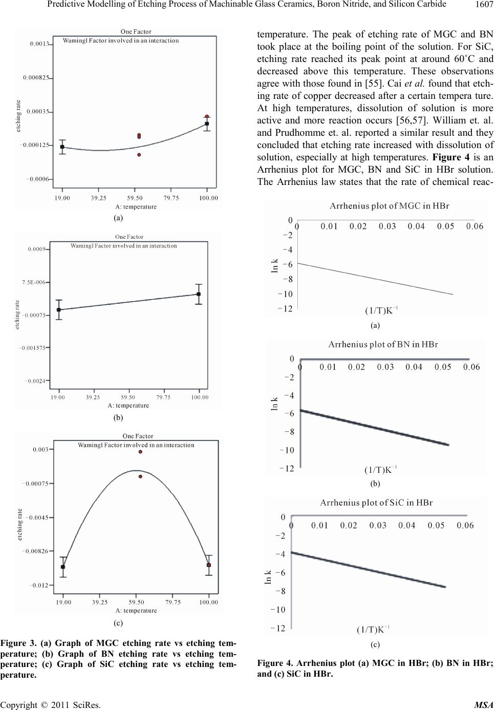 Predictive Modelling of Etching Process of Machinable Glass Ceramics, Boron Nitride, and Silicon Carbide1607 (a) (b) (c) Figure 3. (a) Graph of MGC etching rate vs etching tem- perature; (b) Graph of BN etching rate vs etching tem- perature; (c) Graph of SiC etching rate vs etching tem- perature. temperature. The peak of etching rate of MGC and BN took place at the boiling point of the solution. For SiC, etching rate reached its peak point at around 60˚C and decreased above this temperature. These observations agree with those found in [55]. Cai et al. found that etch- ing rate of copper decreased after a certain tempera ture. At high temperatures, dissolution of solution is more active and more reaction occurs [56,57]. William et. al. and Prudhomme et. al. reported a similar result and they concluded that etching rate increased with dissolution of solution, especially at high temperatures. Figure 4 is an Arrhenius plot for MGC, BN and SiC in HBr solution. The Arrhenius law states that the rate of chemical reac- (a) (b) (c) Figure 4. Arrhenius plot (a) MGC in HBr; (b) BN in HBr; and (c) SiC in HBr. Copyright © 2011 SciRes. MSA  Predictive Modelling of Etching Process of Machinable Glass Ceramics, Boron Nitride, and Silicon Carbide 1608 tion increases exponentially with the absolute tempera- ture [58]. It is well-known that chemical etching proc- esses are limited by either chemical etching reaction or the transport of etchant molec ules by diffusio n. Diffusion limiting processes are relatively insensitive to tempera- ture at lower activation energies and are usually encoun- tered at high concentration [59]. The Arrhenius law’s equation suggests that etching rate increases as the temperature increases. Activation energy, Eo is the minimum amount of energy needed to activate molecules to a condition in which it is equally likely that they will undergo chemical reaction. Table 6 listed the Eo of each material in different etching solu- tions. A similar phenomenon has been observed and re- ported by Vartuli et al. [60] in the case of advanced ce-ramics wet etching, that is, that no etching was found at an etching temperature of 75˚C; Tehrani and Imanian [61] proved that high temperature greatly increased the oxidizing power, which caused a rapid increase in the etching rate; Makino et al. [24] found that all ceramic materials’ tested etching rate was increased with in- creasing etching temperature but less ideal etching be- haviour was also common with more aggressive etching rates [62,63]. The next significant factor is the type of etching solu- tion. The selection of a suitable chemical solution is the key to success. To effectivel y etch a material, we have to make sure the material is compatible with the etching solution for chemical reaction purposes [6]. Figure 5 Illustrates etching rate versus etching solution for MGC, BN and SiC. It shows that the etching rate of MGC and BN in HBr acid was higher compared to that of other solutions; and, the etching rate of SiC in H3PO4 acid was the highest. William et al. [36] summarized a list of che- mical etching process for various materials, etching solu- tions and variables. Their results showed that the etching solution was the main priority to successfully machine the materials. Simon et al. [64] tested four advanced ce- ramics in different etchants and the materials were found to exhibit different etching properties. Three materials were well-etched in molten-salt and one was etched with the electrolytic etching method. Table 6. Ea value of Arr henius plot (kJ/mol). HCl HBr H3PO4 BN 0.1132 0.6037 0.0013 MGC 0.4592 0.6685 0.1329 SiC 0.4978 0.7769 0.1548 (a) (b) (c) Figure 5. (a) Graph of MGC etching rate vs etching solution; (b) Graph of BN etching rate vs etching solution; (c) Graph of SiC etching rate vs etching solution. Copyright © 2011 SciRes. MSA 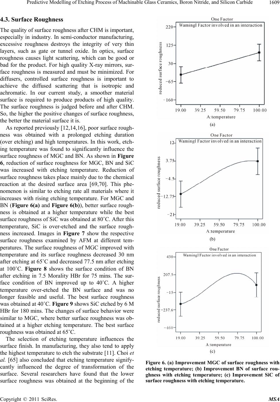 Predictive Modelling of Etching Process of Machinable Glass Ceramics, Boron Nitride, and Silicon Carbide1609 4.3. Surface Roughness The quality of surface roughness after CHM is important, especially in industry. In semi-conductor manufacturing, excessive roughness destroys the integrity of very thin layers, such as gate or tunnel oxide. In optics, surface roughness causes light scattering, which can be good or bad for the product. For high quality X-ray mirrors, sur- face roughness is measured and must be minimized. For diffusers, controlled surface roughness is important to achieve the diffused scattering that is isotropic and achromatic. In our current study, a smoother material surface is required to produce products of high quality. The surface roughness is judged before and after CHM. So, the higher the positive changes of surface roughness, the better the material surface it is. As reported previously [12,14,16], poor surface rough- ness was obtained with a prolonged etching duration (over etching) and high temperatures. In this work, etch- ing temperature was found to significantly influence the surface roughness of MGC and BN. As shown in Figure 6, reduction of surface roughness for MGC, BN and SiC was increased with etching temperature. Reduction of surface roughness takes place mainly due to the chemical reaction at the desired surface area [69,70]. This phe- nomenon is similar to etching rate all materials where it increases with rising etching temperature. For MGC and BN (Figure 6(a) and Figure 6(b)), better surface rough- ness is obtained at a higher temperature while the best surface roughness of SiC was obtained at 80˚C. After this temperature, SiC is over-etched and the surface rough- ness increased. Images in Figure 7 show the respective surface roughness examined by AFM at different tem- peratures. The surface roughness of MGC improved with temperature and its surface roughness decreased 30 nm after etching at 65˚C and decreased 77.5 nm after etching at 100˚C. Figure 8 shows the surface condition of BN after etching in 7.5 Morality HBr for 75 mins. The sur- face condition of BN improved up to 40˚C. A higher temperature over-etched the BN surface and was no longer feasible and useful. The best surface roughness was obtained at 40˚C. Figure 9 shows SiC etched by 6 M HBr for 180 mins. The changes of surface behavior were similar to MGC, where better surface roughness was ob- tained at a higher etching temperature. The best surface roughness was obtained at 65˚C. The selection of etching temperature influences the surface finish. In manufacturing, they also tend to apply the highest temperature to etch the substrate [11]. Choi et al. [65] also concluded that etching temperature signify- cantly influenced the degree of transformation of the surface. Several researchers have found that the lower surface roughness was obtained at the beginning of the (a) (b) (c) Figure 6. (a) Improv ement M GC of surface roughness with etching temperature; (b) Improvement BN of surface rou- ghness with etching temperature; (c) Improvement SiC of surface roughness with etching temperature. Copyright © 2011 SciRes. MSA 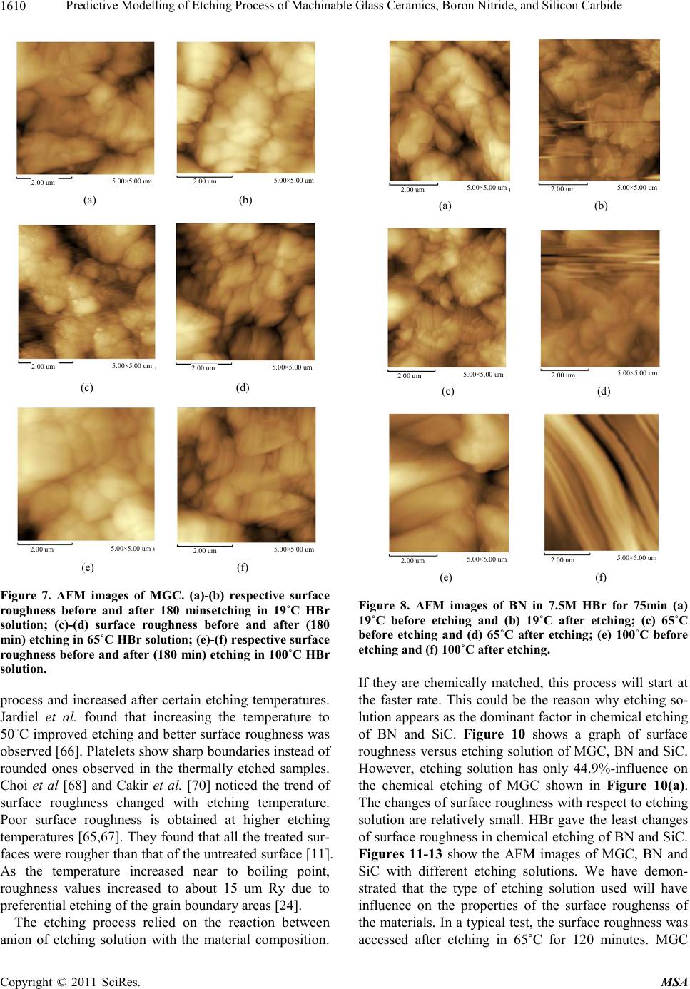 Predictive Modelling of Etching Process of Machinable Glass Ceramics, Boron Nitride, and Silicon Carbide 1610 2.00 um 5.00×5.00 um 2.00 um 5.00×5.00 um (a) (b) 2.00 um 5.00×5.00 um 2.00 um 5.0 0×5.00 um (c) (d) 2.00 um 5.00×5.00 um 2.00 um 5.00×5.00 um (e) (f) Figure 7. AFM images of MGC. (a)-(b) respective surface roughness before and after 180 minsetching in 19˚C HBr solution; (c)-(d) surface roughness before and after (180 min) etching in 65˚C HBr solution; (e)-(f) respective surface roughness before and after (180 min) etching in 100˚C HB r solution. process and increased after certain etching temperatures. Jardiel et al. found that increasing the temperature to 50˚C improved etching and better surface roughness was observed [66]. Platelets show sharp boundaries instead of rounded ones observed in the thermally etched samples. Choi et al [68] and Cakir et al. [70] noticed the trend of surface roughness changed with etching temperature. Poor surface roughness is obtained at higher etching temperatures [65,67]. They found that all the treated sur- faces were rougher than that of the untreated surface [11]. As the temperature increased near to boiling point, roughness values increased to about 15 um Ry due to preferential etching of the grain boundary areas [24]. The etching process relied on the reaction between anion of etching solution with the material composition. 2.00 um5.00×5.00 um 2.00 um 5.00×5.00 um (a) (b) 2.00 um5.00×5.00 um 2.00 um 5.00×5.00 um (c) (d) 2.00 um5.00×5.00 um 2.00 um 5.00×5.00 um (e) (f) Figure 8. AFM images of BN in 7.5M HBr for 75min (a) 19˚C before etching and (b) 19˚C after etching; (c) 65˚C before etching and (d) 65˚C after etching; (e) 100˚C before etching and (f) 100˚C after etching. If they are chemically matched, this process will start at the faster rate. This could be the reason why etching so- lution appears as the dominant factor in chemical etching of BN and SiC. Figure 10 shows a graph of surface rough ness ver sus etchi ng soluti on of MGC, B N and SiC. However, etching solution has only 44.9%-influence on the chemical etching of MGC shown in Figure 10(a). The changes of surface roughness with respect to etching solution are relatively small. HBr gave the least changes of surface roughness in chemical etching of BN and SiC. Figures 11-13 show the AFM images of MGC, BN and SiC with different etching solutions. We have demon- strated that the type of etching solution used will have influence on the properties of the surface roughenss of the materials. In a typical test, the surface roughness was accessed after etching in 65˚C for 120 minutes. MGC Copyright © 2011 SciRes. MSA 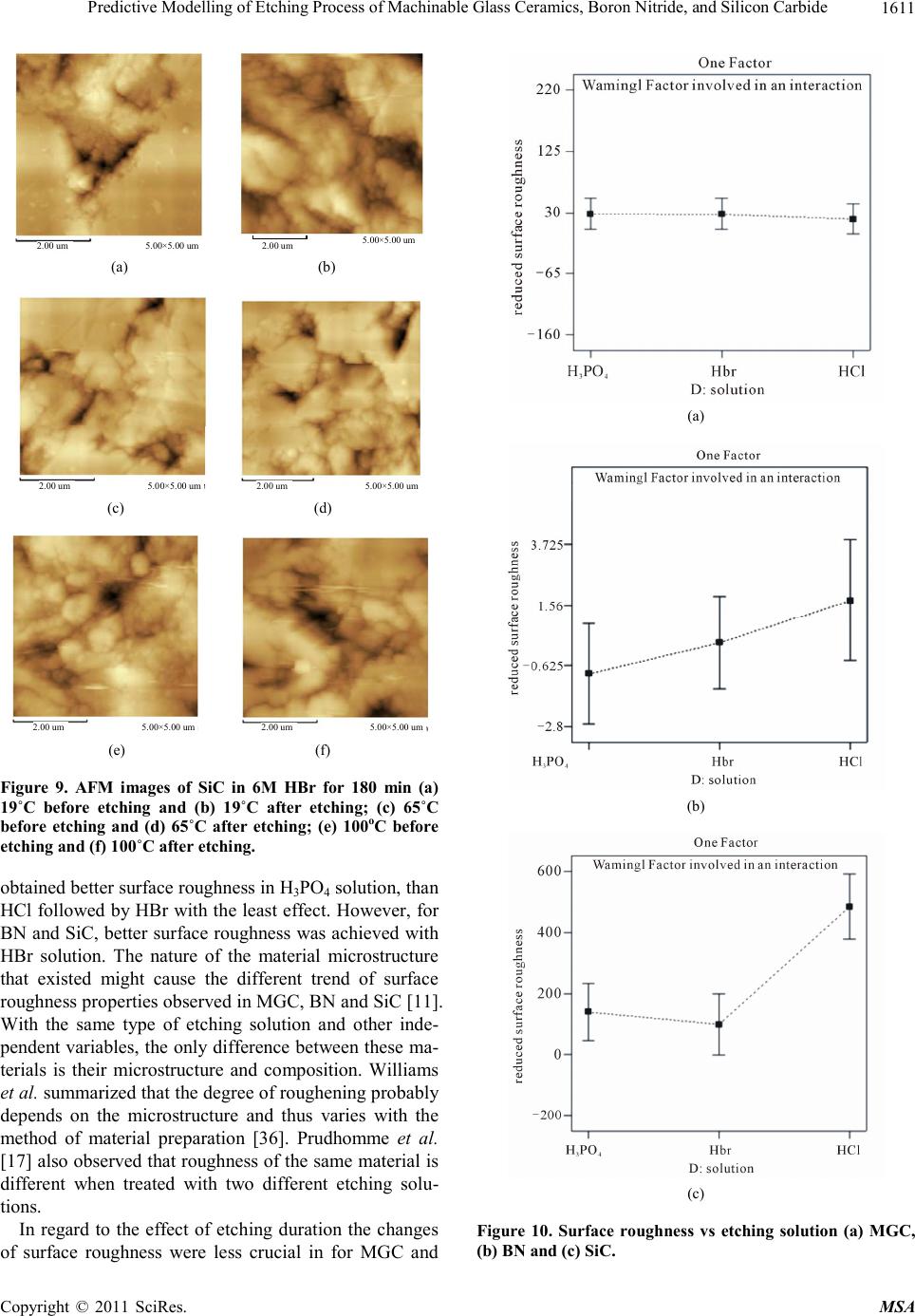 Predictive Modelling of Etching Process of Machinable Glass Ceramics, Boron Nitride, and Silicon Carbide1611 2.00 um 5.00×5.00 um 5.00×5.00 um 2.00 um (a) (b) 2.00 um 5.00×5.00 um 2.00 um 5.00×5.00 um (c) (d) 2.00 um 5.00×5.00 um 2.00 um 5.00×5.00 um (e) (f) Figure 9. AFM images of SiC in 6M HBr for 180 min (a) 19˚C before etching and (b) 19˚C after etching; (c) 65˚C before etching and (d) 65˚C after etching; (e) 100oC before etching and (f) 100˚C after etching. obtained better surface roughness in H3PO4 solutio n, than HCl followed by HBr with the least e ffect. Ho wever, for BN and SiC, better surface roughness was achieved with HBr solution. The nature of the material microstructure that existed might cause the different trend of surface roughness properties observed in MGC, BN and SiC [11]. With the same type of etching solution and other inde- pendent variables, the only difference between these ma- terials is their microstructure and composition. Williams et al. summarized that the degree of roughening probably depends on the microstructure and thus varies with the method of material preparation [36]. Prudhomme et al. [17] also observed that roughness of the same material is different when treated with two different etching solu- tions. In regard to the effect of etching duration the changes of surface roughness were less crucial in for MGC and (a) (b) (c) Figure 10. Surface roughness vs etching solution (a) MGC, (b) BN and (c) SiC. Copyright © 2011 SciRes. MSA 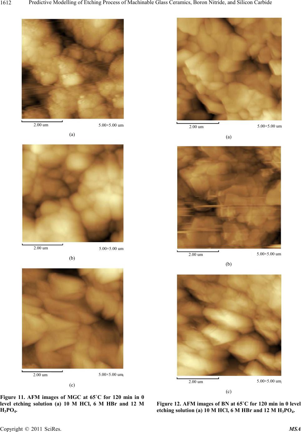 Predictive Modelling of Etching Process of Machinable Glass Ceramics, Boron Nitride, and Silicon Carbide 1612 2.00 um 5.00 ×5 .0 0 u (a) 2.00 u 5.00×5.00 u (b) 2.00 u 5.00×5.00 um (c) Figure 11. AFM images of MGC at 65˚C for 120 min in 0 level etching solution (a) 10 M HCl, 6 M HBr and 12 M H3PO4. 2.00 u 5.00×5.00 um (a) 2.00 u 5.00×5.00 um (b) 2.00 u 5.00×5.00 um (c) Figure 12. AFM images of BN at 65˚C for 120 min in 0 level etching solution (a) 10 M HCl, 6 M HBr and 12 M H3PO4. Copyright © 2011 SciRes. MSA  Predictive Modelling of Etching Process of Machinable Glass Ceramics, Boron Nitride, and Silicon Carbide1613 2.00 u 5.00×5.00 um (a) 2.00 um 5.00×5.00 um (b) 2.00 um 5.00×5. 00 um (c) Figure 13. AFM images of SiC at 65˚C for 120 min in 0 level etching solution (a) 10 M HCl, 6 M HBr and 12 M H3PO4. BN as shown in Figures 14(a) and 14(b) compared to 14(c). Etching duration has a marked influence on sur- face roughness in chemical etching of SiC. This is shown clearly in Figure 14(c) where surface roughness dra- matically increases with increasing etching duration. The changes of surface roughness were slow in the beginning probably due to material dissolution that resulted in re- duction of chemical reaction. Prudhomme et al. [57] and Cakir et al. [11,67] reported similar results. Better sur- face roughness was found at higher etching duration. Improvement in the surface state occurred when the sol- ute was dissolved in the etching solution at a longer etching period, which increases the energy gap for gen- erating etch figure and reduces the damage of material’s surface. Baranova and Dorosinskii [68] found that as the duration of etching increased, insoluble reaction products started forming and eroded the surface thus causing the samples to be no longer suitable for further study. Etch- ing time is important while longer etching period pro- duced a constant etching process in the case of alumin- ium etching, because dissolution of chemical solution was not completed at the beginning of the process. After this period, the etching process was observed to be more stable [67]. 4.4. Effect of Indentation Industrial patterning involves designing and producing a desirable pattern on the material surface. Method of nano-patterning includes dry and wet mask patterning. The selection of mask for patterning in CHM is an issue due to the difficulties associated with the quality of the mask and increasing demand for multi-kind and small- quantity production in a market. In overcoming these difficulties, a new technology has been introduced to replace mask patterning by micro-indentation. This tech- nique enhanced versatility and provided lower cost for initial facilities and manufacture, simplicity of process and material selectivity [12,13,69-71]. Typically, 5N load (P = 500 Nm–2) is applied on the material surface where patterning is required and then followed by etch- ing process. By applying the load onto the desired area, it is thought to enhance the bonding of the material struc- ture and delay the chemical reaction happens at the in- dented area At the end of the process, measurement is taken at indented area and non-indented area [36]. The indented area will become convex after etching. The etching ratio comprising the relative etching rate between that of non-indented area and indented area was then compared. Patterning is successfully created when etch- ing rate at non-indented area is higher than etching rate at indented area. The higher the etching ratio is the better the feasibility of the patterning process. One of the key points of this technology is inducing an etching rate Copyright © 2011 SciRes. MSA  Predictive Modelling of Etching Process of Machinable Glass Ceramics, Boron Nitride, and Silicon Carbide 1614 (a) (b) (c) Figure 14. Improvement of surface roughness vs etching duration in HBr solution (a) MGC; (b) BN and (c) SiC. change arising from the indentation [13]. Patterning is successfully created when etching rate at non-indented area is higher than etching rate at indented area. A convex is built when e above phenomena takes place. One of the most significant factors is the material properties, which resulted from the production method and subsequent processing. The convex is created by applying a load onto the desired spot. By applying the load onto this area, it is enhancing the bonding of the material structure and delaying the chemical reaction happening at the indented area [36]. A higher etching ratio is preferred where higher etching rate occurred at the non-indented area and lower etching rate at the in- dented area. The etching duration was found to be the most signify- cant variable in etching ratio and Figure 15 shows a plot etching rate of indented and non-indented area for MGC, BN and SiC so l utio n. I t sho ws t hat t he highe st d iffe re nce between indented and non-indented area occurs mostly at 200 min. This observation is consistent with the etching rate results shown in Table 4, where etching rate is in- creased with etching duration. The reduction of etching rate at the longer etching duration is possibly due to the insoluble deposit formed at the indented area [13]. A peak etching ratio is found in the etching of BN at 90 min (Figure 16(a)). Etching rate at non-indented area was found to be higher compared to etching rate at in- dented area, especially at high temperature. This also indicates that etching depth is dependent on time, where one would expect a square root of time dependence for etching depth and a much lower activation energy [72]. Cakir et al. observed that etching ratio of non-indented to indented area increased with etching process. Similar phenomena are observed in many research works [12,13, 69-71]. Nagai et al. [15] successfully conducted experi- ments on macro-size patterning and chemical etching, which led to the formation of well-ordered patterns of surface crystal steps. Youn and Kang [12] fabricated Py- rex glass by micro-indentation with HF etching. Saito et al. [13,69,70] proved the feasibility of micro-machining process in fabricating glass ceramic in HF etching. These research works showed that patterning on the glass ce- ramic surface becomes possible due to etching rate dif- ference between indented and non-indented area. One of the key challenges of this technology is to increase and control etching rate difference between indented and non-indented area. With less than 0.05 p-value, solution concentration is the main factor that is able to influence the etching ratio of MGC, BN and SiC. Figure 17 shows the graph of etching ratio vs solution concentration. Overall, etching ratio is decreased with etching duration. A peak etching ratio is found in the etching of BN, which is around Copyright © 2011 SciRes. MSA  Predictive Modelling of Etching Process of Machinable Glass Ceramics, Boron Nitride, and Silicon Carbide1615 (a) (b) (c) Figure 15. Etching rate of indented area and non-indented area vs etching duration (HCl solution) (a) MGC; (b) BN and (c) SiC. –0.50 or 6 M HBr. This implied that higher etching rate difference between non-indented and indented area could be obtained in lower solution concentration. The result sugge sts t hat, i n hi gher sol uti on co ncentr at ion r egio n, th e (a) (b) (c) Figure 16. Etching ratio vs etching duration (HCl solution) (a) MGC; (b) BN and (c) SiC. Copyright © 2011 SciRes. MSA  Predictive Modelling of Etching Process of Machinable Glass Ceramics, Boron Nitride, and Silicon Carbide 1616 (a) (b) (c) Figure 17 . Etching ratio vs sol u tion conc entratio n (a) M GC; (b) BN and (c) SiC. leaching reaction scarcely occurred even at non-indented area, resulting in a decrease of etching rate ratio. The etching reaction of the material and the leaching reaction are considered to be competitive reaction. When the leaching precedes the etching reaction, the etching rate would be increased. Saito et al. found etching ratio for glass ceramic was obtained at lower pH region [13,69]. They also suggested that etching ratio can be controlled by solution concentration. Saito et al. [70] also reported that not only alkali and alkali earth metal oxide, but also alumina in alumina silicate glass was leached out in HF acid. 4.5. Predic tive Mod el s Predictive models generated by RSM are presented in (3) to (11), where t is etching duration, T is etching tem- perature, c is solution concentration. These are empirical models and can be applied in the industry for mass pro- duction. For MGC, etching rate (ER) H3PO4 ER0.000257 0.00000430.0000012 0.00013 0.0000015 0.0000225 exp2 Tt cTc c (3) HBr ER0.00004 0.00000090.0000007 0.000130.00000150.000023 exp2 Tt cTcc (4) HCI ER0.000047 0.00000060.000059 0.00000150.0000225 exp2 Tc Tc c (5) For MGC, improvement of surface roughness (SR) H3PO4 SR69.95 0.8030.09511.9 0.0047 0.00410.395 Td TtTc tc c Tc c c c c (6) HBr SR74 0.7590.28689.80.405 0.0047 0.395 Ttc Tt tc (7) HCI SR5.005 0.3230.235119.22 0.0047 0.4050.395 Tt Tt Tctc (8) For MGC, etching ratio (R) H3PO4 R1.91 0.0420.0231.40 0.00026 0.0230.0057 Tt Tt Tctc (9) HBr R0.0042 0.0170.0290.68 0.00026 0.0230.0057 Tt Tt Tctc (10) HCI R2.16 0.0420.0270.85 0.00026 0.0230.0057 Tt Tt Tctc (11) 5. Comparison between ANN and RSM After determining ANN p rogramme and RSM predictive model, the two techniques were then compared. This is Copyright © 2011 SciRes. MSA 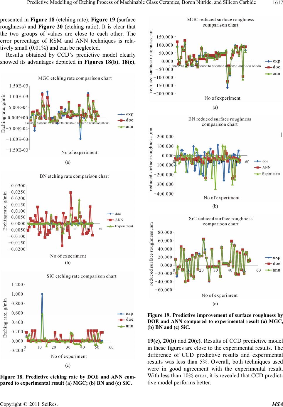 Predictive Modelling of Etching Process of Machinable Glass Ceramics, Boron Nitride, and Silicon Carbide1617 presented in Figure 18 (etching rate), Figure 19 (surface roughness) and Figure 20 (etching ratio). It is clear that the two groups of values are close to each other. The error percentage of RSM and ANN techniques is rela- tively small (0.01%) and can be neglected. Results obtained by CCD’s predictive model clearly showed its advantages depicted in Figures 18(b), 18(c), (a) (b) (c) Figure 18. Predictive etching rate by DOE and ANN com- pared to experimental result (a) MGC; (b) BN and (c) SiC. (a) (b) (c) Figure 19. Predictive improvement of surface roughness by DOE and ANN compared to experimental result (a) MGC, (b) BN and (c) SiC. 19(c), 20(b) and 20(c). Results of CCD pr edictive model in these figures are close to the experimental results. The difference of CCD predictive results and experimental results was less than 5%. Overall, both techniques used were in good agreement with the experimental result. With less than 10% error, it is revealed that CCD predict- tive model performs better. Copyright © 2011 SciRes. MSA  Predictive Modelling of Etching Process of Machinable Glass Ceramics, Boron Nitride, and Silicon Carbide 1618 (a) (b) (c) Figure 20. Predictive etching ratio by DOE and ANN com- pared to experimental result (a) MGC; (b) BN and (c) SiC. 6. Optimization Table 7 shows the optimization for each material. As a result, HBr based etch recipe provides the fastest yet controllable results in the etching of MGC. The optimum of HBr based etch recipe happened at 100˚C, with dura- tion of 30 mins and 8.5 Molarity of HBr, where etch rate is 0.0011 g/min, surface improvement, 80.879 nm and etching ratio, 3.277. Table 7. Optimization of etching rate, surface roughness and etchi ng ratio. MGC Desirability 0.586 0.392 0.240 Solution HBr HCl H3PO4 Temperature (˚C) 100 100 100 Duration (min) 30 30 109 Concentration (Molarity) 8.5 10.5 9.5 Etching rate (g/min) 0.001 0.001 0.0003 Surface rou ghness (improvement ) (u/min) 80.79 81.82 87.23 BN Desirability 0.5624 0.3367 0.2425 Solution HBr HCl H3PO4 Temperature (˚C) 40 100 25 Duration (min) 62 128 137 Concentration (Molarity) 6.0 9.5 9.5 Etching rate (g/min) 0.0003 0.005 0.0002 Surface rou ghness (improvement ) (u/min) <0.001 <0.001 <0.001 Etching ratio 3.153 0.533 1.45 SiC Desirability 0.954 0.525 0.419 Solution HBr H3PO4 HCl Temperature (˚C) 75 100 74 Duration (min) 240 172 240 Concentration (Molarity) 8.5 9.5 10.5 Etching rate (g/min) 0.001 0.012 0.0003 Surface rou ghness (improvement ) (u/min) 128.71 34.17 62.786 Etching ratio 10.00 2.12 8.59 7. Conclusions In summary, we have successfully conducted CHM on MGC, BN and SiC. The results supported the feasibility of wet chemical micro-patterning of advanced ceramics for micro-devices applications. Direct patterning is suc- cessfully introduced to meet the increasingly vocal de- mand for multi-kind and small quantity production. In this leading-edge of research involving the use of micro- and nanotechnology, more flexible patterning techniques are desired. The following concluding remarks can be drawn. Copyright © 2011 SciRes. MSA  Predictive Modelling of Etching Process of Machinable Glass Ceramics, Boron Nitride, and Silicon Carbide1619 1) CCD as a technique for design of experiment pro- vides useful statistically results in analyzing the chemical etching process of advanced ceramics. 2) Use of ANN in predicting the etching results were found to be effective. These results were in good agree- ment with those predicted by RSM. One of the disadvan- tages is that more time is needed in looking for the suit- able transfer function. 3) The relationships between etching rate, surface roughness and etching ratio with etching temperature, etching duration, etching solution and solution concen- tration were successfull y established. 4) The optimum chemical etching process was carried out with the optimization technique provided by DE 7. The etching rate and improvement of surface quality achieved is 0.0011 g/min, 80.789 nm respectively and the etching ratio is 3.277. 8. Acknowledgements The authors would like to acknowledge the support given by Ministry of Science, Technology and Innovation (Ma- laysia) MOSTI, and Curtin University-Sara wak Malaysia. REFERENCES [1] E. P. DeGarmo, J. T. B. R. A. Kohser and B. E. Klamecki, “Materials and Processes in Manufacturing,” 9th Edition, John Wiley & Sons, Inc., Hoboken, 2003. [2] J. Y. Thompson, S. C. Bayne and H. O. Heymann, “Me- chanical Properties of a New Mica-Based Machinable Glass Ceramic for C AD/CAM Resto ration s,” Th e Jou rna l of Prosthetic Dentistry, Vol. 76, No. 3, 1996, pp. 619-623. doi:10.1016/S0022-3913(96)90440-0 [3] A. Guedes, et al., “Multilayered Interface in Ti/Macor Machinable Glass-Ceramics Joints,” Materials Science and Engineering A, Vol. 301, 2001, pp . 118-124. doi:10.1016/S0921-5093(00)01804-9 [4] A. F. Grogan and D. F . Smart, “C eramic Surfaces for Tri- bological Components,” Materials and Design, Vol. 2, 1981, pp . 197-201. doi:10.1016/0261-3069(81)90020-0 [5] ASM, “Metals Handbook Machining,” Vol. 16, ASM Interna tional Pub licati on, 1989. [6] C. T. Lynch, “CRC Handbook of Materials Science,” 2nd Edition, CRC Press, C.T. Lynch, 1975. [7] D. M. Allen, “The Principles and Practice of Photo- chemical Machining and Photoetching,” Adam Hil- ger/IOP, UK, 1986. [8] E. V. Zakka, Constantoudis and E. Gogolides, “Rough- ness Formation during Plasma Etching of Composite Materials: A Kinetic Monte Carlo Approach,” IEEE Transactions of Plasma Science, Vol. 35, No. 5, 2007, pp. 1359-1369. doi:10.1109/TPS.2007.906135 [9] F. Gao, et al. , “Chan ging the Size an d Shape of Ge Island by Chemical Etching,” Journal of Crystal Growth, Vol. 231, No. 1-2, 2001, pp. 17-21. doi:10.1016/S0022-0248(01)01357-4 [10] U. Gilabert, A. B. Trigubo and N. E. W. D. Reca, “Chemical Etch in g o f CdZnTe (11 1) Surfaces,” Materials Science and Engineering B, Vol. 27, No. 2-3, 1994, pp. L11-15. doi:10.1016/0921-5107(94)90138-4 [11] O. Cakir, H. Temel and M. Kiyak, “Chemical Etching of Cu-ETP Copper,” Journal of Materials Processing Tech- nology, Vol. 162-1 63 , 200 5, pp . 275- 279. doi:10.1016/j.jmatprotec.2005.02.035 [12] S. W. Youn and C. G. K., “Maskless Pattern Fabrication on Pyrex 7740 Glass Surface by Using Nano-Scrat ch with HF Wet Etching,” Scripta Materialia, Vol. 52, 2005, pp. 117-122. doi:10.1016/j.scriptamat.2004.09.016 [13] Y. Saito, et al., “Mechanism of Etching Rate Change of Aluminosilicate Glass in HF Acid with Micro-Indentati- on,” Applied Surface Science, Vol. 255, 2008, pp. 2290- 2294. doi:10.1016/j.apsusc.2008.07.085 [14] Y. Saito, et al., “Fabrication of Micro-Structure on Glass Surface Using Micro-Indentation and Wet etching Proc- ess,” Applied Surface Science, Vol. 254, 2008, pp. 7243-7249. doi:10.1016/j.apsusc.2008.05.320 [15] T. Nagai,.A. Imanishi and Y. Nakato, “Scratch Induced Nano-Wires Acting as a Macro-Pattern fro Formation of Well-Ordered Step Structures on H-Terminated Si (111) by Chemical Etchin g,” Applied Surface Science, Vol. 237, No. 1-4, 2004, pp. 533-537. doi:10.1016/j .apsusc. 2004.06.122 [16] P. G. Benardos and G.-C. Vosniakos, “Predicting Surface Roughness in Machining: A Review,” International Jou- rnal of Machine Tools Manufacture, Vol. 43, 2003, pp. 833-844. doi:10.1016/S0890-6955(03)00059-2 [17] N. P r udhomme, et al ., “Design of High Frequency GaPO4 BAW Resonators b y Chemical Etchin g,” Sensors and Ac- tuators B, Vol. 13 1, 20 08, pp. 270-278. doi:10.1016/j.snb.2007.11.020 [18] J. Weber, et al., “Hydrogen Penetration into Silicon dur- ing Wet-Chemical Etching,” Microelectronic Engineering, Vol. 66, 2003, pp. 320-326. doi:10.1016/S0167-9317(02)00926-7 [19] C. Lin, et al., “A Fast Phototyping Proc ess fo r Fabrication of Microfluidic Systems on Soda-Lime Glass,” Journal of Micromechanics and Microengineering, Vol. 11, 2001, pp. 726- 732. doi:10.1088/0960-1317/11/6/316 [20] D. C. S. Bien, et al., “Chracterizati on of Masking Materi - als for Deep Glass Micromachining,” Journal of Micro- elec tr ome c hanic al Sy s te ms , Vol. 13, 2 0 03, pp. S34-S40. [21] J. Zhang, et al., “Polymerization Optimization of SU-8 Photoresist and its Application in Microfluidic Systems and MEMS,” Journal of Micromechanics and Microen- gineering, Vol. 11, 2001, pp. 20-26. do i :10.10 88/096 0-1317/11/1/304 [22] T. Corman, P. Enoksson and G. Stemme, “Deep Wet Etching of Borosilicate Glass Using an Anodically Bonded Silicon Substrate as Mask,” Journal of Micro- mechanics and Microengineering, Vol. 8, 19 98. [23] A. Berthold, P. M. Sarro and M. J. Vellekoop, “Two-Step Copyright © 2011 SciRes. MSA  Predictive Modelling of Etching Process of Machinable Glass Ceramics, Boron Nitride, and Silicon Carbide 1620 Glass Wet-Etching for Micro-Fluidic Devices,” Proceed- ings of the SeSens Workshop, Veldhoven, 2000. [24] E. Makino, T. Shibata and Y. Yamada, “Micromachin- ing of Fine Ceramics by Photolithography,” Sensors and Actuators A, Vol . 75, 1 99 9, pp. 278-288. doi:10.1016/S0924-4247(98)00353-7 [25] X. Li, T. Abe and M. Esashi, “Fabrication of High-Den- sity Electrical Feed-Throughs by Deep-Reactive-Ion Et- ching of Pyrex Glass,” Journal of Microelectromechani- cal Syst ems, Vol. 1-6, 2002, pp. 625-630. [26] H. Wensink, et al., “High Resolution Powder Blasting Micromachining,” Proceeding of the 13th Annual Inter- national Conference on Micro Electro Mechanical Sys- tems, Miyazaki, 2000. [27] Y. S. Liao and L. C. Chen, “A Method of Etching and Powder Blasting for Microholes,” Journal of Materials Processing Technology, 2009 . [28] S. Schlautmann, et al., “Powder-Blasting Technology as an Alternative Tool for Microfabrication of Capilllary Electrophoresis Chips with Integrated Conductivity Sen- sors,” Journal of Micromechanics and Microengineering, Vol. 11, 2001, pp. 386-389. do i :10.10 88/096 0-1317/11/4/318 [29] T. Abe, X. Li and M. Esashi, “Endpoint Detectable Plat- ing through Femtosecond Laser Drilled Glass Wafers for Electrical Interconnections,” Sensors and Actuators A, Vol. 108, 2003 , pp. 23 4-238 . doi:10.1016/S0924-4247(03)00262-0 [30] C.-W. Chang and C.-P. Kuo, “An Investigation of La- ser-Assisted Machin ing of Al2O3 Ceramics Planning,” In- ternational Journal of Machine Tools and Manufacture, Vol. 47, 2007, pp. 452-461. [31] C.-H. Tsai and H.-W. Chen, “Laser Milling of Cavity in Ceramic Substrate by Fracture Machining Element Tech- nique,” Journal of Materials Processing Technology, V ol . 136, 2003, pp. 158-165. doi:10.1016/S0924-0136(03)00133-X [32] L. Chen, E. Siores and W. C. K. Wong, “Keft Character- istics in Abrasive Water Jet Machining of alumina Ce- ramics,” International Journal of Machine Tools and Manufacture, Vol. 36, 1996, pp. 1 20 1-1206. do i :10.10 16/0890-6955(95) 00108-5 [33] Z. J. Pei, et al., “Rotary Ultrasonic Machining for Face Milling of Ceramics,” International Journal of Machine Tools Manufacture, Vol. 35, No. 7, 1995, pp. 1033-1046. do i :10.10 16/0890-6955(94) 00100-X [34] I. P. Tuersley, A. Jawaid and I. R. Pashby, “Review: Various Methods of Machining Advanced Ceramics Ma- terials,” Journal of Materials Processing Technology, Vol. 42, 1994, pp. 377-390 . do i :10.10 16/0924-0136(94) 90144-9 [35] T. Watanabe, “Mass Production of Quartz High-Speed Chemical Etching Applied to AT-Cut Wafers,” IEEE In- ternational Frequency Control Symposium and PDA Ex- hibition, 2001, pp. 36 8- 3 75. [36] K. R. Williams, K. Gupta and M. Wasilik, “Etch Rates for Micromachining Processing-Part 2,” Journal of Mi- croelectromechanical Systems, Vol. 12, No. 6, 2003, pp. 761-778. doi:10.1109/JMEMS.2003.820936 [37] F. Gaiseanu, et al., “Chemical Etching Control during the Self-Limitation Process by Boron Diffusion in Silicon: Analytical Results,” Proceeding of 19 97 IEEE Semicon- duct or Conference, 1997, pp. 247-250. [38] Y. Minhao, M. J. Henderson and A. Gibaud, “On the Etching of Silica and Mesoporous Silica Films Deter- mined by X-ray Reflectivity and Atomic Force Micros- copy,” Thin Solid Films, Vol. 514, 2009, pp. 3028-3035. doi:10.1016/j.tsf.2008.12.017 [39] M. E. Olsen, et al., “Effect of Varying Etching Times on the Bond Strength of Ceramic Brackets,” American Journal of Orthodontics and Dentofacial Orthopedics, Vol. 109, No. 4, 1996, pp. 403-409. doi:10.1016/S0889-5406(96)70122-1 [40] D. C. Montgomerty, “Design and Analysis of Experi- ment,” 5th Edition, John Wiley & Sons, Inc., 2001. [41] M. J. Anderson and P. J. Whitcomb, “RSM Simplified: Optimizing Processes Using Response Surface Methods for Design of Experiments,” 2nd Edition, Productivity Press, New York, 2005. [42] M. J. Anderson and P. J. Whitcomb, “DOE Simplified: Practical Tools for Effective Experimentation,” 2nd Edi- tion, Productivity Press, New York, 2007. [43] S. Baldassari, et al., “DOE Analyses on Aqueous Sus- pendsions of TiO2 Nanoparticles,” Journal of European Ceramic Society, Vol. 28, 2008, pp. 2665-2671. doi:10.1016/j.jeurceramsoc.2008.03.044 [44] C. Pierlot, et al., “Design of Experiments in Thermal Spraying: A Review,” Surface and Coatings Technology, Vol. 202, 2008, pp. 4483-4490. doi:10.1016/j.surfcoat.2008.04.031 [45] S. Subramanian, et al., “Modeling and Optimization of the Chemical Etching Process in Niobium Cavities,” In- ternational Congress on Advanced Nuclear Power, Hol- lywood, Florida, 2002. [46] P. H. Chen, et al., “Application of the Taguchi’s Design of Experients to Optimize a Bromine Chemistry-Based Etching Recipe for Deep Silicon Trenches,” Microel ec- tronic Engineering, Vol. 77, 2005, pp. 110-115. doi:10.1016/j.mee.2004.09.001 [47] M. A. Dabnun, M. S. J. Hashmi and M. A. El-Baradie, “Surface Roughness Predictive Model by Design of Ex- periments for Turning Machinable Glass-Ceramic (Ma- cor),” Journal of Materials Processing Technology, Vol. 164-165, 2005, pp. 1289-1293. doi:10.1016/j.jmatprotec.2005.02.062 [48] M. D. Mathew, D. W. Kim and W.-S. Ryu, “A Neural Network Model to Predict Low Cycle Fatigue Life of Ni- trogen-Alloyed 316L Stainless Steel,” Materials Science and Engineering A, Vol. 474, 2008, pp . 247-253. doi:10.1016/j.msea.2007.04.018 [49] M. Smith, “Neural Networks for Statistic Modeling,” Van Nostrand Reinhold, New York, 1993. [50] T. W. Liao, “Modelling Process Mean and Variation with Copyright © 2011 SciRes. MSA  Predictive Modelling of Etching Process of Machinable Glass Ceramics, Boron Nitride, and Silicon Carbide Copyright © 2011 SciRes. MSA 1621 MLP Neural Networks,” International Journal of Ma- chine Tools Manufacture, Vol. 36, No. 12, 1996, pp. 1307-1319. doi:10.1016/S0890-6955(96)00054-5 [51] K. Hornik, M. Stinchcombe and H. White, “Multilayer Feedforward Networks Neural Networks,” IEEE Transac- tion on Neutral Network, Vol. 2, 1989, pp . 359-366. [52] K. Funahashi, “On the Approximate Realization of Con- tinuous Mappings by Neural Networks,” Neural networks, Vol. 2, 1989, pp. 183-192. do i :10.10 16/0893-6080(89) 90003-8 [53] K. Hornik, “Approximation Capabilities of Mulitlayer Feedforward Networks,” Neural networks, Vol. 4, 1991, pp. 251- 257. doi:10.1016/0893-6080(91)90009-T [54] M. Aydinalp-Koksal and V. I. Ugursal, “Comparison of Neural Netwok, Conditional Demand Analysis, and Engi- neering Approaches for Modelling End-Use Energy Con- sumption in the Residential Sector,” Applied Energy, Vol. 85, 2008, pp. 271-296 . doi:10.1016/j.apenergy.2006.09.012 [55] J. Cai, et al ., “Effects on Etching Rates of Copper in Fer- ric Chloride Solutions,” IEMT/IMC P r oceedin g, 1998. [56] K. R. Williams and R. S. Muller, “Etch Rates for Micro- machining Processing,” Journal of Microelectrome- chanical Systems, Vol. 5, No. 4, 1996, pp. 256-269. do i :10.11 09/84.5464 06 [57] N. Prudhomme, et al., “Gallium Orthophoshate Device Manufacturing by Chemical Etching,” Proceeding of 2003 IEEE International Frequency Control Symposium and PDA Exhibition, 2003, pp. 68 8- 6 93. [58] P. L. Houston, “Chemical Kinetics and Reaction Dy- namoics,” 1st Edition, McGraw-Hill, 2001. [59] C. S. Sundararaman, A. Mouton and J. F. Currie, “Che- mical Etching of InP. Indium Phosphide and Related Ma- terials,” 2nd International Conference Proceeding, 1990, pp. 224-227. [60] C. B. Vartuli, et al., “Wet Chemical Etching Survey of III-Nitrides. Solid-State Electronics,” Vol. 41, No. 12, 1997, pp. 194 7- 1 95 4. doi:10.1016/S0038-1101(97)00173-1 [61] A. F. Tehrani and E. Imanian, “A New Etchant for the Chemical Machining of St304,” Journal of Materials Processing Technology, Vol. 149, 2004, pp. 404-408. doi:10.1016/j.jmatprotec.2004.02.055 [62] Y. Hua, “Studies of a New Chemical Etching Method- 152 Secco Etch in Failure Analysis of Wafer Fabrica- tion,” Proceeding in ICSE, 1998, pp. 20- 2 6. [63] I. Virginia Semiconductor, “Wet-Chemical Etching and Cleaning of Silicon,” Virginia Semicondcutor, Inc: Fred- ericksburg, 2003. [64] S. G. Cook, J. A. Little and J. E. King, “Etching and Mi- crostructure of Engineering Ceramics,” Materials Char- acterization, Vol. 34, No. 1, 19 95, pp. 1-8. do i :10.10 16/1044-5803(94) 00044-L [65] H.-J. Choi, et al., “Sliding Wear of Silicon Carbide Modi- fied by Etching with Chlorine at Various Temperatures,” Wear, Vol. 266, 2009, pp. 214 - 21 9. do i :10.10 16/j. wear. 2008 .06.0 21 [66] T. Jardiel, et al., “Domain Structure of Bi4Ti3O12 Ceram- ics Revealed by Chemical Etch ing,” Journal of European Ceramic Society, Vol. 26, 2006, pp. 2823-2826. doi:10.1016/j.jeurceramsoc.2005.05.003 [67] O. Cakir, “Chemical Etching of Aluminium,” Journal of Materials Processing Technology, Vol. 199, 2008, pp. 337-340. doi:10.1016/j.jmatprotec.2007.08.012 [68] G. K. Baranova and L. A. Dorosinskii, “Chemical Polish- ing and E tching of Bi-Sr-Ca-Cu-O High Temperatu re Su- perconduting System,” Physica C, Vol. 194, 1992, pp. 425-429. doi:10.1016/S0921-4534(05)80024-3 [69] Y. Saito, et al., “Micro-Fabrication Techniques Applied to Alumino silicate Glass Surface s: Micro- Indentation an d Wet Etchi ng Pro cess,” Thin Solid Films, Vol. 517, No. 2, 2009, pp. 2900-290 4. doi:10.1016/j.tsf.2008.11.077 [70] Y. Saito, et al., “Fabrication of Micro-Structure on Glass Surface Using Micro-Indentation and Wet Etching Proc- ess,” Applied Surface Science, Vol. 254, 2008, pp. 7243-7237. doi:10.1016/j.apsusc.2008.05.320 [71] O. Cakir, A. Y. T. Ozben, “Chemical Machining,” Ar- chives of Materials Science and Engineering, Vol. 28, No. 8, 2007, pp. 499-502. [72] J. Peng, et al., “Micro-Patterning of 0.70Pb (Mg1/3Nb2/3) O3-0.30Pb Ti O3 Single Crystals by Ultrasonic Wet Chemical Et ching,” Materia ls letters, Vol. 62, No. 17-18, 2008, pp. 3127-313 0. doi:10.1016/j.matlet.2008.02.003
|