P. WHIG ET AL.
Copyright © 2011 SciRes. IJCNS
717
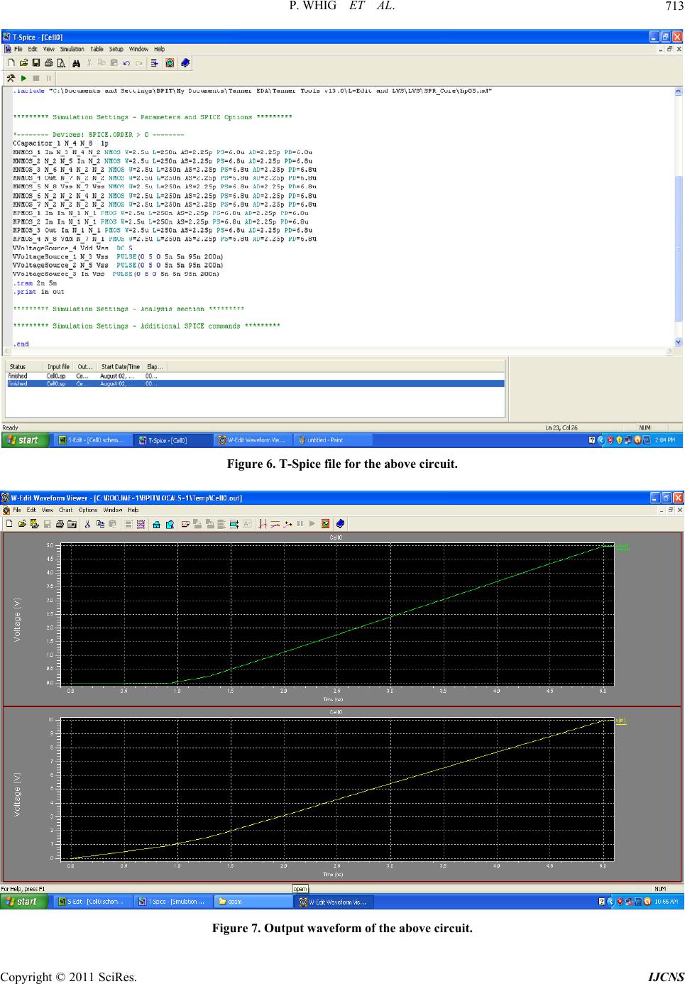
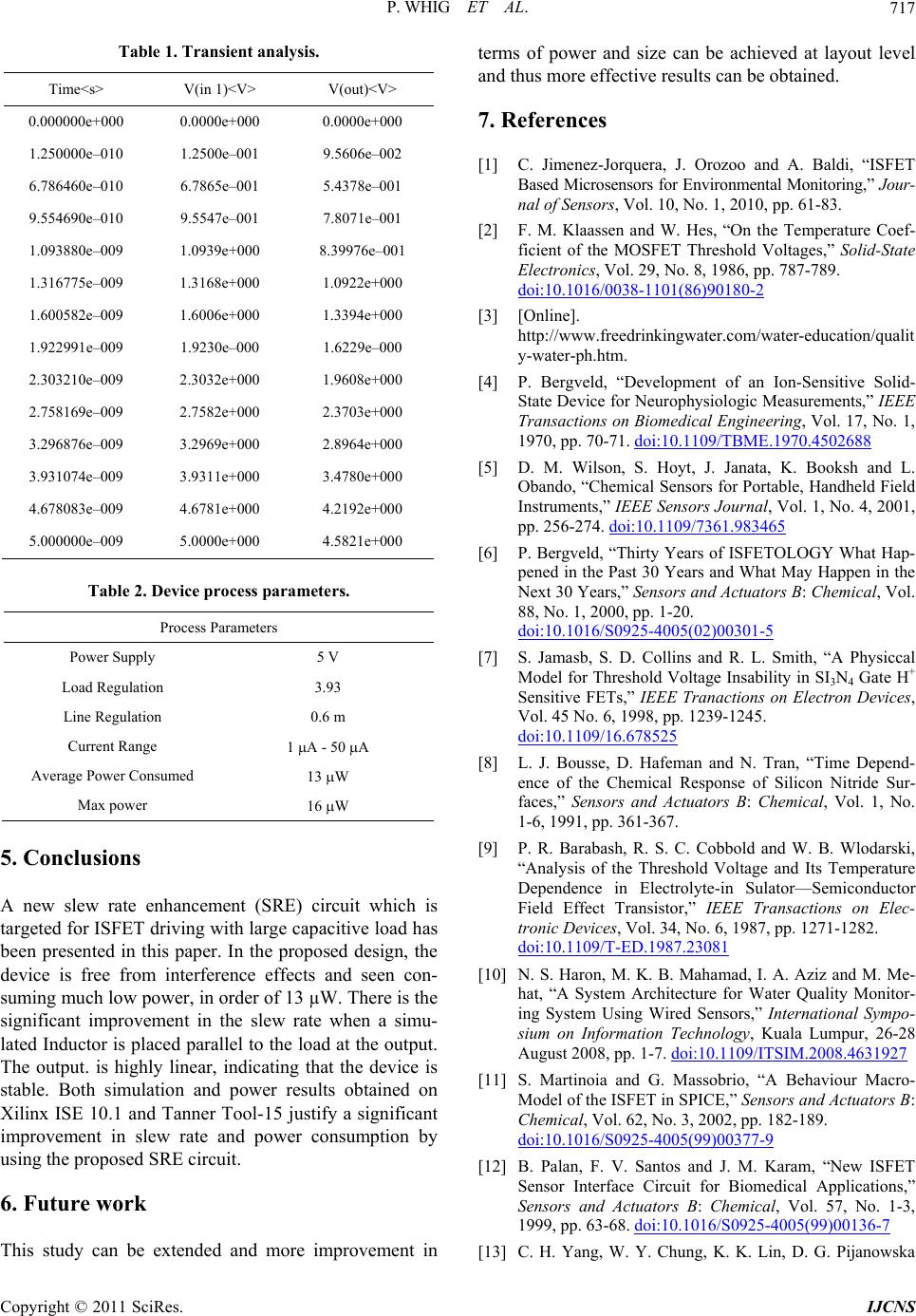
Table 1. Transient analysis.
Time<s> V(in 1)<V> V(out)<V>
0.000000e+000 0.0000e+000 0.0000e+000
1.250000e–010 1.2500e–001 9.5606e–002
6.786460e–010 6.7865e–001 5.4378e–001
9.554690e–010 9.5547e–001 7.8071e–001
1.093880e–009 1.0939e+000 8.39976e–001
1.316775e–009 1.3168e+000 1.0922e+000
1.600582e–009 1.6006e+000 1.3394e+000
1.922991e–009 1.9230e–000 1.6229e–000
2.303210e–009 2.3032e+000 1.9608e+000
2.758169e–009 2.7582e+000 2.3703e+000
3.296876e–009 3.2969e+000 2.8964e+000
3.931074e–009 3.9311e+000 3.4780e+000
4.678083e–009 4.6781e+000 4.2192e+000
5.000000e–009 5.0000e+000 4.5821e+000
Table 2. Device process parameters.
Process Parameters
Power Supply 5 V
Load Regulation 3.93
Line Regulation 0.6 m
Current Range 1 A - 50 A
Average Power Consumed 13 W
Max power 16 W
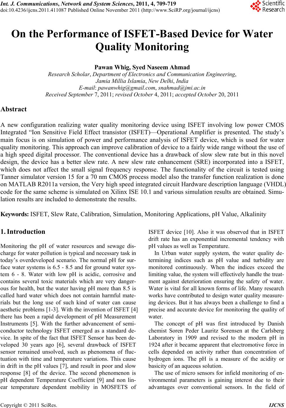
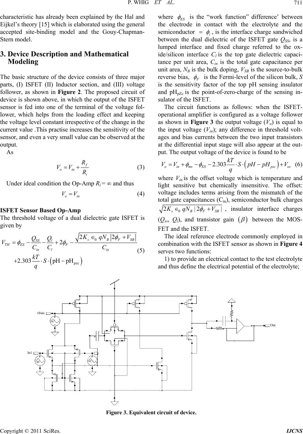
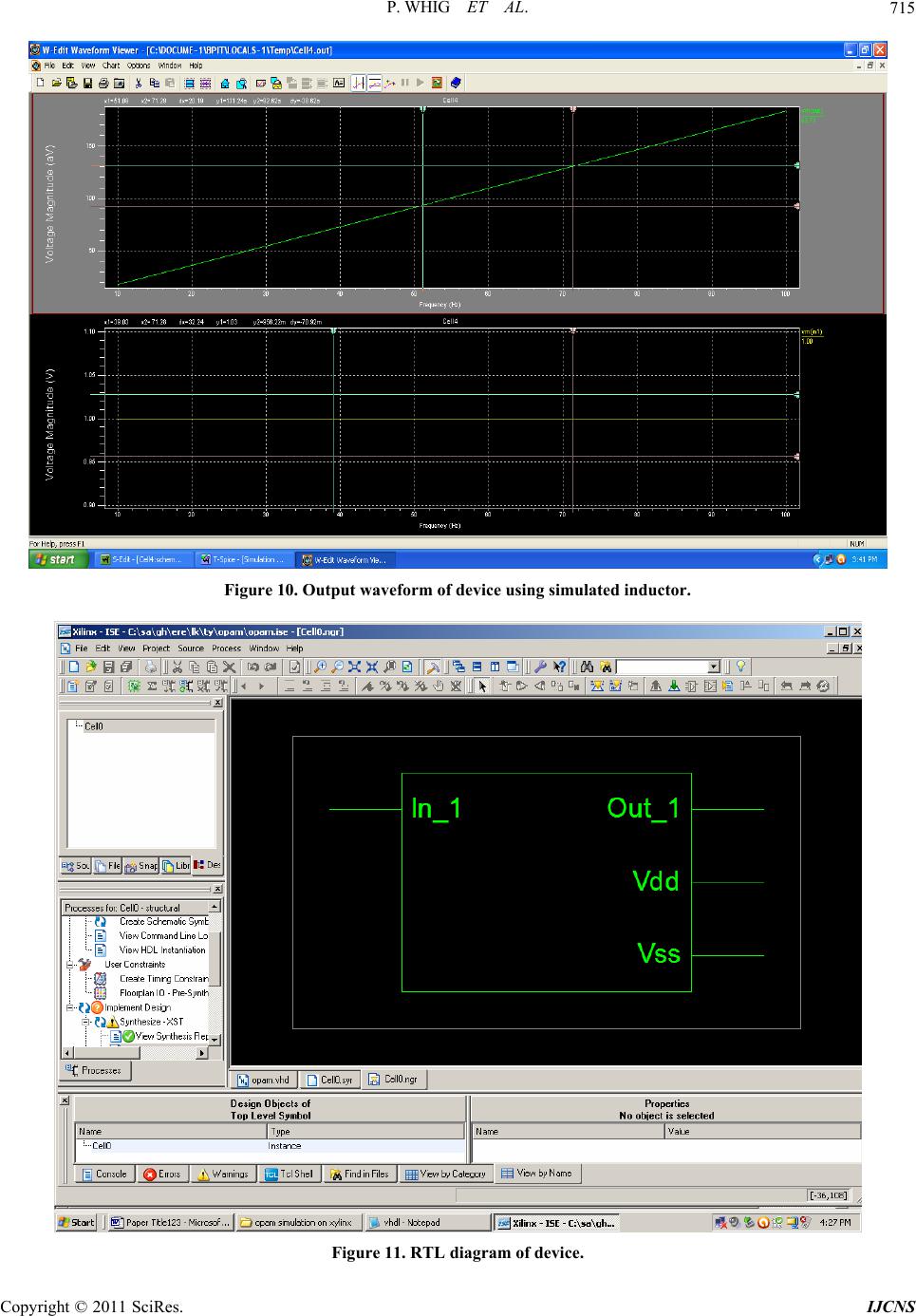
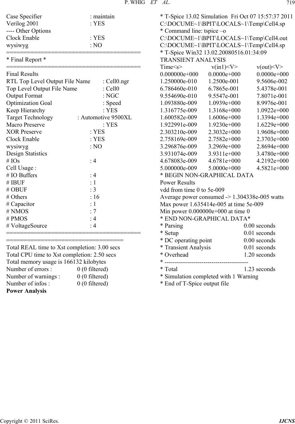
5. Conclusions
A new slew rate enhancement (SRE) circuit which is
targeted for ISFET driving with large capacitive load has
been presented in this paper. In the proposed design, the
device is free from interference effects and seen con-
suming much low power, in order of 13 µW. There is the
significant improvement in the slew rate when a simu-
lated Inductor is placed parallel to the load at the output.
The output. is highly linear, indicating that the device is
stable. Both simulation and power results obtained on
Xilinx ISE 10.1 and Tanner Tool-15 justify a significant
improvement in slew rate and power consumption by
using the proposed SRE circuit.
6. Future work
This study can be extended and more improvement in
terms of power and size can be achieved at layout level
and thus more effective results can be obtained.
7. References
[1] C. Jimenez-Jorquera, J. Orozoo and A. Baldi, “ISFET
Based Microsensors for Environmental Monitoring,” Jour-
nal of Sensors, Vol. 10, No. 1, 2010, pp. 61-83.
[2] F. M. Klaassen and W. Hes, “On the Temperature Coef-
ficient of the MOSFET Threshold Voltages,” Solid-State
Electronics, Vol. 29, No. 8, 1986, pp. 787-789.
doi:10.1016/0038-1101(86)90180-2
[3] [Online].
http://www.freedrinkingwater.com/water-education/qualit
y-water-ph.htm.
[4] P. Bergveld, “Development of an Ion-Sensitive Solid-
State Device for Neurophysiologic Measurements,” IEEE
Transactions on Biomedical Engineering, Vol. 17, No. 1,
1970, pp. 70-71. doi:10.1109/TBME.1970.4502688
[5] D. M. Wilson, S. Hoyt, J. Janata, K. Booksh and L.
Obando, “Chemical Sensors for Portable, Handheld Field
Instruments,” IEEE Sensors Journal, Vol. 1, No. 4, 2001,
pp. 256-274. doi:10.1109/7361.983465
[6] P. Bergveld, “Thirty Years of ISFETOLOGY What Hap-
pened in the Past 30 Years and What May Happen in the
Next 30 Years,” Sensors and Actuators B: Chemical, Vol.
88, No. 1, 2000, pp. 1-20.
doi:10.1016/S0925-4005(02)00301-5
[7] S. Jamasb, S. D. Collins and R. L. Smith, “A Physiccal
Model for Threshold Voltage Insability in SI3N4 Gate H+
Sensitive FETs,” IEEE Tranactions on Electron Devices,
Vol. 45 No. 6, 1998, pp. 1239-1245.
doi:10.1109/16.678525
[8] L. J. Bousse, D. Hafeman and N. Tran, “Time Depend-
ence of the Chemical Response of Silicon Nitride Sur-
faces,” Sensors and Actuators B: Chemical, Vol. 1, No.
1-6, 1991, pp. 361-367.
[9] P. R. Barabash, R. S. C. Cobbold and W. B. Wlodarski,
“Analysis of the Threshold Voltage and Its Temperature
Dependence in Electrolyte-in Sulator—Semiconductor
Field Effect Transistor,” IEEE Transactions on Elec-
tronic Devices, Vol. 34, No. 6, 1987, pp. 1271-1282.
doi:10.1109/T-ED.1987.23081
[10] N. S. Haron, M. K. B. Mahamad, I. A. Aziz and M. Me-
hat, “A System Architecture for Water Quality Monitor-
ing System Using Wired Sensors,” International Sympo-
sium on Information Technology, Kuala Lumpur, 26-28
August 2008, pp. 1-7. doi:10.1109/ITSIM.2008.4631927
[11] S. Martinoia and G. Massobrio, “A Behaviour Macro-
Model of the ISFET in SPICE,” Sensors and Actuators B:
Chemical, Vol. 62, No. 3, 2002, pp. 182-189.
doi:10.1016/S0925-4005(99)00377-9
[12] B. Palan, F. V. Santos and J. M. Karam, “New ISFET
Sensor Interface Circuit for Biomedical Applications,”
Sensors and Actuators B: Chemical, Vol. 57, No. 1-3,
1999, pp. 63-68. doi:10.1016/S0925-4005(99)00136-7
[13] C. H. Yang, W. Y. Chung, K. K. Lin, D. G. Pijanowska