Journal of Materials Science and Chemical Engineering
Vol.06 No.01(2018), Article ID:81573,7 pages
10.4236/msce.2018.61004
Surface Roughness of SiGe/Si(110) Formed by Stress-Induced Twins and the Solution to Produce Smooth Surface
Junji Yamanaka1, Mai Shirakura1, Chiaya Yamamoto1,2, Naoto Utsuyama3, Kei Sato3, Takane Yamada3, Kosuke O. Hara3, Keisuke Arimoto3, Kiyokazu Nakagawa3
1Center for Instrumental Analysis, University of Yamanashi, Kofu, Japan
2Center for Creative Technology, University of Yamanashi, Kofu, Japan
3Center for Crystal Science and Technology, University of Yamanashi, Kofu, Japan


Received: September 16, 2017; Accepted: January 1, 2018; Published: January 4, 2018
ABSTRACT
Lattice-strained Si thin films grown onto SiGe(110)/Si(110) are attracting because of their potential to realize high-speed transistors. In this study we observe surface morphology of Si/SiGe/Si(110) using scanning electron microscopy and we also observe microstructure of the identical position using cross-sectional transmission electron microscopy. These results reveal that crossing of stress-induced twins causes remarkable surface roughness. We propose using vicinal substrate to avoid this phenomenon and our successive experimental results are shown in this paper.
Keywords:
Strained Si, SiGe(110), Stress-Induced Twin, Transmission Electron Microscopy

1. Introduction
In order to produce a high-speed field-effect-transistor (FET), strain control of semiconductor thin films are very important because elastically strained semiconductors sometimes show very high carrier mobility. Therefore many research groups in the world carried out both theoretical and experimental works on this view-point. Especially strained-Si grown onto SiGe(110) Si(110) is considered to be a promising material for complementary metal oxide semiconductor (CMOS) circuits [1]-[14]. Recently K. Arimoto and other members of our group have been studied the crystal-growth mechanism of lattice-strained-Si/lattice-relaxed-SiGe/ Si(110) hetero-structure [12] [13] [14]. These studies showed us that stress-induced twins were introduced during the SiGe growth and they had an important role to relax the SiGe buffer layers and to form strained Si layers. However, some specimens showed remarkable surface roughness. We must avoid surface roughening to produce a high-speed FET because of the well-known negative effect of the interface scattering.
The purpose of this study is identifying the origin of this remarkable surface roughness observed on Si/SiGe(110)/Si(110). We also challenge to produce a Si/SiGe/Si(110) with flat surface.
2. Experimental Procedure
Commercially available Si(110) wafers were used as substrates after chemical and thermal cleaning. Then we deposited thin films onto the Si(110) using solid-source-MBE. At first compositionally step-graded SiGe layers were deposited. Then uniform SiGe layers, and after that, the top Si layers were deposited. The substrates’ temperature was 600˚C. The total thickness of the SiGe buffer layers were 400 - 800 nm. The thickness of the top Si layer was 20 nm. The growth rate of the film was about 0.1 - 2 A/sec. Surface morphology of the specimens was observed by atomic force microscope (AFM) and scanning electron microscope (SEM). After these observations, we coated the specimens with protection layersto avoid ion-bombardment of focused ion beam (FIB). The 1st protection layer was permanent marker’s ink. The 2nd one was a sputtered Pt-Pd. The 3rd and final one was a W layer. Then we picked up a part of the specimens and thinned them using FIB. After that we observed the micro-structure of the specimens using transmission electron microscopes (TEM). After the FIB and the TEM, we chemically removed the protection layers from some of the specimens and observed surface morphology again using SEM to make clear where the cross-sectional TEM data were taken from. (We used the ink, which can be solved by using acetone, as the 1st protection layer for this purpose.)
3. Results and Discussion
First, surface morphology of the specimens was observed by AFM. A typical AFM image is shown in Figure 1. We also took scanning electron micrograph and its typical result is shown in Figure 2. Straight lines along [110] direction are seen in both images. It has been already known through our previous works that these line are the result of stress induced twins. The important point of these images shown in Figure 1 and Figure 2 is thick remarkable roughness which are also parallel to [110] direction. The widths of the thick roughness are submicron or micron orders. These roughness must effect negatively when we produce a FET, therefore it is very important to know the origin of them and to reduce them.
Figure 3 is a wide range plan-view SEM image. A red rectangle are was picked up for cross-sectional TEM observation using FIB.
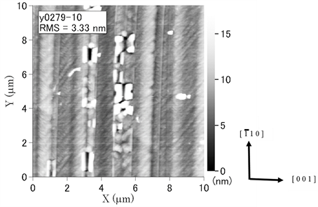
Figure 1. A typical AFM image of the specimen surface.
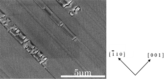
Figure 2. A typical SEM image of the specimen surface.
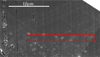
Figure 3. A wide view SEM image of the specimen surface. Red rectangle area was used for cross-sectional TEM observation (see Figure 4).
Figure 4 is the TEM image taken from the red-rectangle area in the Figure 3. We took several TEM images adjacent each other and the combined one is shown in the Figure 4. It is clear that there are crossing of the stress-induced twins under the surface where the thick remarkable rough area can be seen in the plan-view SEM image (compare Figure 3 and Figure 4). The plan-view SEM observation and the cross-sectional TEM observation of the identical position reveals that the origin of the thick roughing band is the crossing of the stress-induced twins.
Figure 5 shows a set of precise TEM observations of the area where the stress-induced twins are crossing each other. (The observed are of the Figure 5 is not shown in Figure 4, but it is close to the area shown in Figure 4.) The dark field TEM images (DFI) in Figure 5 show that the crystallographic orientations of the twins are same even after the crossing. However, more important information is as follows: The DFI in Figure 5 show that the original stress-induced twins are quit thin (less than 20 nm thick), but after the crossing the twins show
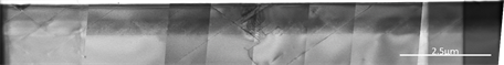
Figure 4. A wide range cross-sectional TEM image. The TEM specimen for this observation was picked up from the red rectangle area shown in Figure 3.
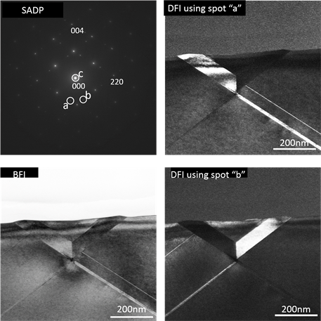
Figure 5. TEM observations of the area where the stress-induced twins are crossing each other. SADP: a selected area electron diffraction taken from the area around the bright field image in this figure. BFI: a bright field TEM image. DFIs: dark filed TEM images using the spots “a” and “c” in the SADP.
thicker (about 100 nm) widths than the original ones. The specimen surface of the two thick twins and the region sandwiched by the twins do not show flat morphology.
Figure 6 shows a TEM bright field image, narrow area (~200 nm) selected diffraction patterns (SADPs), and high-resolution transmission electron micrographs (HREMs) taken from the same area of Figure 5. The SADPs in Figure 6 approve that the crystallographic orientations of the twins are same even after the crossing as mentioned before using the results of Figure 5. The HREM shown in Figure 6(F) shows that the thick twin just under the specimen-surface was made up of many thin twins which have only several {111} planes, although it is not clear whether or not this fact is related to the surface roughening.
The HREM around the crossing point of the stress-induced twins, which is shown in Figure 6(E), was taken in order to analyze what happened at the point. This HREM shows the atomic-layer stacking is always as same as the original crystal or twin crystals. The scientific reason of this experimental fact is not known yet and further experiments and discussions are needed.
Now it is revealed that the crossing of the stress-induced twins cause remarkable
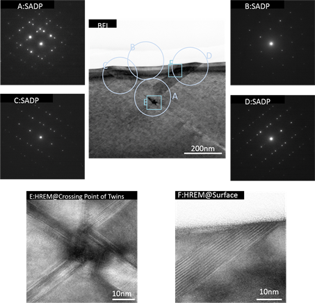
Figure 6. TEM data taken from the identical position with area of Figure 5. BFI: a bright field image. In this case the incidental beam condition was parallel to the zone axis, therefore the image contrast is different from that of the BFI in Figure 5. (A), (B), (C), (D): SADPs from the corresponding area shown in the BFI. (E), (F): HREMs from the corresponding area shown in the BFI.
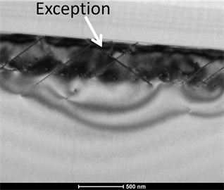
Figure 7. A bright field TEM of the specimen deposited onto a vicinal substrate.
thick rough band on the specimen surface. There still exists a room for scientific discussion to understand the origin of this phenomena, however, it is clear that we can produce a smoother surface if we can reduce the crossing of the twins. K. Arimoto and other members of our group have already had the technique to reduce the crossing of the stress-induced twins through our previous works for other purpose [10] [11] [12] [13] [14]. The stress-induced twins were formed along one kind of {111} plane when we used vicinal substrate because the stresses onto the (111) and on the ( ) are different [12]. In this study, we can apply this technique onto our new specimens. Figure 7 is a bright field TEM image of the specimen deposited onto a vicinal substrate. It is clearly seen that the density of the crossing twins are drastically reduced because almost all twin are parallel, although there still exist very small amount of twins which have a different direction.
4. Summary
We observed the surface morphology of Si/SiGe/Si(110) mainly using scanning electron microscopy and we also observed microstructure of the specimens using cross-sectional transmission electron microscopy. Through these precise observations, the following results were shown:
1) The plan-view SEM observation and the cross-sectional TEM observation of the identical position reveal that the origin of the thick roughing band is the crossing of the stress-induced twins.
2) The twins keep their crystallographic orientations even after crossing each other. On the other hand, the widths of the twins drastically increase after the crossing.
3) We succeeded in reducing the density of the twin-crossing by using vicinal substrate.
Cite this paper
Yamanaka, J., Shirakura, M., Yamamoto, C., Utsuyama, N., Sato, K., Yamada, T., Hara, K.O., Arimoto, K. and Nakagawa, K. (2018) Surface Roughness of SiGe/Si(110) Formed by Stress-Induced Twins and the Solution to Produce Smooth Surface. Journal of Materials Science and Chemical Engineering, 6, 25-31. https://doi.org/10.4236/msce.2018.61004
References
- 1. Mizuno, T., Sugiyama, N., Tezuka, T., Moriyama, Y., Nakaharai, S. and Takagi, S. (2005) -Surface Strained-SOI CMOS Devices. IEEE Transactions on Electron Devices, 52, 367-374. https://doi.org/10.1109/TED.2005.843894
- 2. Teramoto, A., et al. (2007) Very High Carrier Mobility for High-Performance CMOS on a Si(110) Surface. IEEE Transactions on Electron Devices, 54, 1438-1445. https://doi.org/10.1109/TED.2007.896372
- 3. Kuan, T.S. and Iyer, S.S. (1991) Strain Relaxation and Ordering in SiGe Layers Grown on (100), (111), and (110) Si Surfaces by Molecular-Beam Epitaxy. Appl. Phys. Lett., 59, 2242. https://doi.org/10.1063/1.106083
- 4. Hartmann, J.M., Burdin, M., Rolland, G. and Billon, T. (2006) Growth Kinetics of Si and SiGe on Si(1 0 0), Si(1 1 0) and Si(1 1 1) Surfaces. J. Cryst. Growth, 294, 288-295. https://doi.org/10.1016/j.jcrysgro.2006.06.043
- 5. Destefanis, V., Hartmann, J.M., Abbadie, A., Papon, A.M. and Billon, T. (2009) Growth and Structural Properties of SiGe Virtual Substrates on Si(1 0 0), (1 1 0) and (1 1 1). J. Cryst. Growth, 311, 1070-1079. https://doi.org/10.1016/j.jcrysgro.2008.12.034
- 6. Destefanis, V., Rouchon, D., Hartmann, J.M., Crisci, A., Papon, A.M., Baud, L. and Mermoux, M. (2009) Structural Properties of Tensily Strained Si Layers Grown on SiGe(100), (110), and (111) Virtual Substrates. J. Appl. Phys., 106 043508. https://doi.org/10.1063/1.3187925
- 7. Arimoto, K., et al. (2009) Structural and Transport Properties of Strained SiGe Grown on V-Groove Patterned Si(110) Substrates. J. Cryst. Growth, 311, 814-818. https://doi.org/10.1016/j.jcrysgro.2008.09.062
- 8. Arimoto, K., et al. (2017) Hole Mobility in Strained Si/SiGe/Vicinal Si(110) Grown by Gas Source MBE. J. Cryst. Growth, 468, 625-629. https://doi.org/10.1016/j.jcrysgro.2016.12.076
- 9. Kato, M., Arimoto, K., Yamanaka, J., Nakagawa, K. and Sawano, K. (Available Online 24 May 2017) Fabrication of High-Quality Strain Relaxed SiGe (1 1 0) Films by Controlling Defects via Ion Implantation. J. Cryst. Growth, in Press.
- 10. Arimoto, K., et al. (2006) Determination of Lattice Parameters of SiGe/Si(110) Heterostructures. Thin Solid Films, 508, 132-135. https://doi.org/10.1016/j.tsf.2005.08.412
- 11. Arimoto, K., et al. (2007) Growth Temperature Dependence of Lattice Structures of SiGe/Graded Buffer Structures Grown on Si(110) Substrates by Gas-Source MBE. J. Cryst. Growth, 301-302, 343-348. https://doi.org/10.1016/j.jcrysgro.2006.11.135
- 12. Arimoto, K., et al. (2007) Crystalline Morphologies of Step-Graded SiGe Layers Grown on Exact and Vicinal (110) Si Substrates. J. Cryst. Growth, 311, 809-813. https://doi.org/10.1016/j.jcrysgro.2008.09.061
- 13. Arimoto, K., et al. (2009) Strain Relaxation Mechanisms in Step-Graded SiGe/ Si(110) Heterostructures Grown by Gas-Source MBE at High Temperatures. J. Cryst. Growth, 311, 819-824. https://doi.org/10.1016/j.jcrysgro.2008.09.064
- 14. Arimoto, K., et al. (2013) Formation of Compressively Strained SiGe/Si(110) Heterostructures and Their Characterization. J. Cryst. Growth, 362, 282-287. https://doi.org/10.1016/j.jcrysgro.2011.12.082