Circuits and Systems, 2011, 2, 326-329
doi:10.4236/cs.2011.24045 Published Online October 2011 (http://www.scirp.org/journal/cs)
Copyright © 2011 SciRes. CS
Analysis of 8T SRAM Cell at Various Process
Corners at 65 nm Process Technology
Shilpi Birla1*, Neeraj Kumar Shukla2, Kapil Rathi3, Rakesh Kumar Singh4, Manisha Pattanaik5
1Department of Electronics & Communications, Sir Pa d am p at Singhania Universi t y, Udaipur, India
2Department of ECE, ITM University, Gurgaon, India
3Texas Instruments, Bangalore, India
4Department of Electronics & Communications, Bipin Chandra Tripathi kumaon Engineering College, Almora, India
5VLSI Group, Atal Bihari Vajpayee Ind ian Institute of Information Technology and Management, Gwalior, India
E-mail: *shilpibirla@gmail.com
Received June 7, 2011; revised July 22, 2011; accepted July 29, 2011
Abstract
In Present scenario battery-powered hand-held multimedia systems become popular. The power consumption
in these devices is a major concern these days for its long operational life. Although various techniques to
reduce the power dissipation has been developed. The most adopted method is to lower the supply voltage.
But lowering the Vdd reduces the gate current much more rapidly than the sub-threshold current and degrades
the SNM. This degraded SNM further limits the voltage scaling. To improve the stability of the SRAM cell
topology of the conventional 6T Static Random Access Memory (SRAM) cell has been changed and revised
to 8T and 10T cell, the topologies. This work has analyzed the SRAM’s Static Noise Margin (SNM) at 8T
for various process corners at 65 nm technology. It evaluates the SNM along with the write margins of the
cell along with the cell size of 8T SRAM bit-cell operating in sub-threshold voltage at various process cor-
ners. It is observed that an 8T cell has 13% better write margin than conventional 6T SRAM cell. This paper
analyses the dependence of SNM of SRAM memory cell on supply voltage, temperature, transistor sizing in
65 nm technology at various process corners (TT, SS, FF, FS, and SF).
Keywords: SNM, Sub-Threshold Current, Gate Current, Process Corners
1. Introduction
Due to increase in demand of wireless sensor nodes and
mobile multimedia applications, the demand of small
size SRAM memory on chips increases. However, as the
voltage is scaled down to combat the rise in power and
other issues, e.g., the lower noise margins (responsible
for cell stability) arise in conventional 6T SRAM cells.
Solutions involving additional transistors, i.e., 7T, and
8T have been explored to lower power consumption
while reducing these adverse effects in the cell perform-
ance. We will therefore look into one of these SRAM
Cells topologies, the 8T SRAM cell which operates at
sub-threshold voltages, successfully. The ultra-low leak-
age regime for static random-access memories (SRAM)
designs imposes unique constraints on the cell design in
many ways different from those imposed by perform-
ance-driven scaling concerns. The bit-cell size is of
paramount importance regardless of the device threshold
voltage but beyond that the similarity ends. The high
threshold voltage associated with the ultra-low leakage
design point provides sub stantial relief to the static noise
margin (SNM) for a given design, but the intrinsic thre-
shold variation limits the performance availab le from the
cell [1]. The intrinsic threshold variation affects the lea-
kage as well, but in a less significant manner. In this pa-
per we have analyzed the Static Noise Margin (SNM) of
8T SRAM cell at various process corners of the design
environment at 65 nm.
This paper is organized as follows; SNM is described
in section II. Section III deals with the working of 8T
SRAM cell. Section IV shows the analysis of SNM, Write
margin, Read Margin with respect to various process
corners. Finally, concl usi on is drawn in section V.
2. Static Noise Margin
The best measure of the ability of these inverters to
S. BIRLA ET AL.
Copyright © 2011 SciRes. CS
327
maintain their states is the bit-cell’s SNM. The SNM is
the maximum amount of noise voltage that can be intro-
duced at the output of the two inverters, such that the cell
retains its data. SNM quanties the amount of noise vol-
tage required at the internal nod es of a bit-cell to ip th e
cell’s contents [2]. The static noise margin is a measure
of the cell’s ability to retain its data state. The worst-case
situation is usually under “read-disturb” condition [3].
When the word-line device is turned on and connects the
pre-charged bit-line to the low side of the cell. The state
of the cell may flip if the internal node voltage rises to a
high enough level. The problem is exacerbated if the
ratio of the conductance of the pull-down and the word-
line devices (often called beta) is too small.
3. Analysis of 8T SRAM Cell
This topology was originally proposed for a sub-thresh-
old SRAM design. It is optimized for functionality and
performance over a large voltage range in this design.
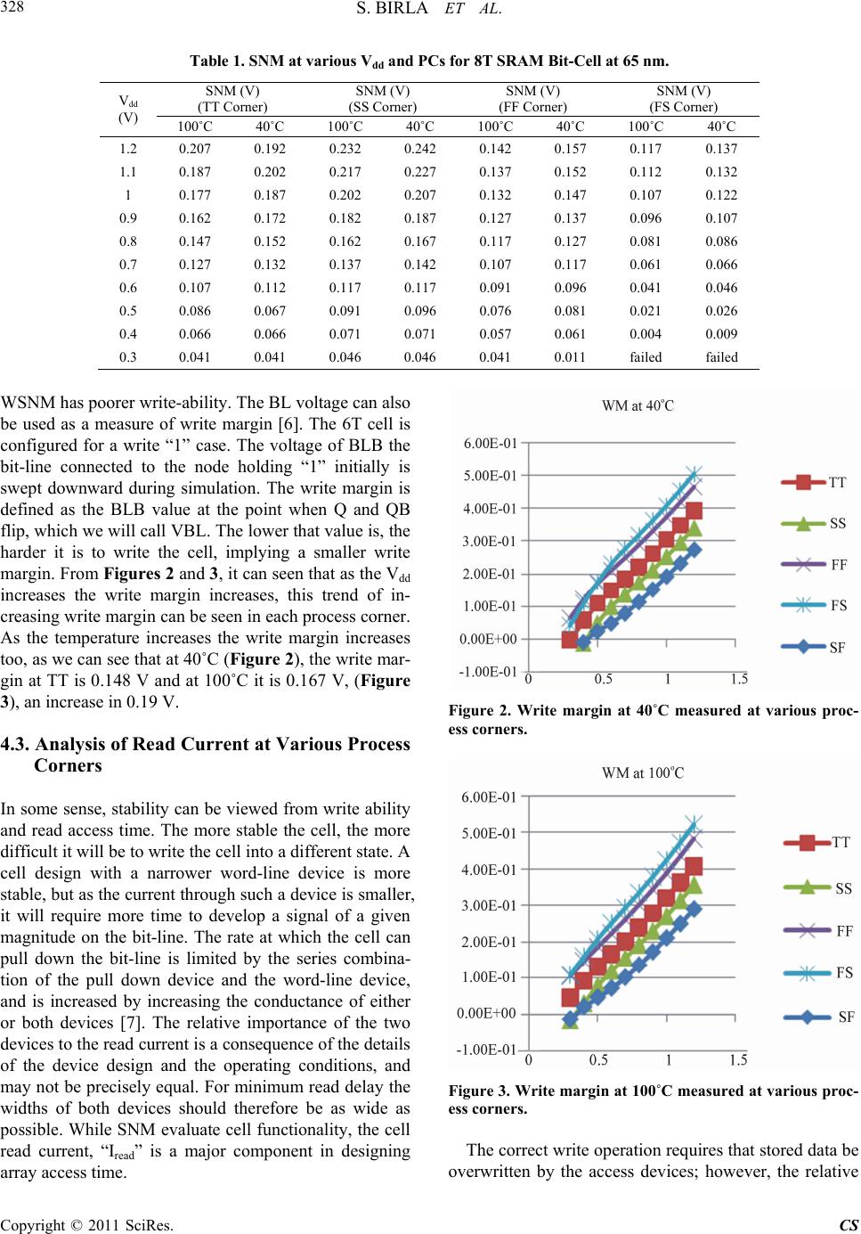
Two NMOS devices (N3 and N2), Figure 1, constitute
the read-buffer. A write operation is performed through
WWL, WBL and WBLX ports, whereas single-ended
read operation is exercised through RWL and RBL ports.
RBL is pre-charged at the end of each read cycle and
kept pre-charged during a write cycle [4]. In th is bit-cell,
read and write ports are decoupled in contrast to the tra-
ditional 6T cell so that the,
1) read-SNM (RSNM) problem is eliminated;
2) 6T SRAM part can be sized for better write-ability
without trading-off RSNM and;
3) 2T read-buffer can be sized for larger read-current
independently.
This makes the voltage drop across unaccessed read-
buffers zero and hence leakage on read-bit-lines is highly
reduced. Vdd is the virtual supply nodes for the cross-
coupled inverters and its voltage can be brought down
during a write access to weaken PMOS load devices (P1
and P2), Figure 1, and ease write-ability problem at low
voltages. Since all the bit-cells on a row are written and
NM2
VDD
WWL
PM1 PM0
NM1
WLB
NM3
WBLX
NM0
Q’
VSS
RBL
RWL
NM4
NM5
Figure 1. 8T SRAM Cell.
read at the same time, Vdd is shared across one row of
memory cells [5].
4. Analysis at Different Process Corners
Process Corners (PCs) represent the extremes of these
parameter variations within which a circuit that has been
etched onto the wafer must function correctly. A circuit
running on devices fabricated at these process corners
may run slower or faster than specified and at lower or
higher temperatures and voltages, but if the circuit does
not function at all at any of these process extremes the
design is considered to have inadequate design margin.
There are therefore five possible process corners: typi-
cal-typical (TT), fast-fast (FF), slow-slow (SS), fast-slow
(FS), and slow-fast (SF). The first three corners (TT, FF,
SS) are called even corners, because both types of de-
vices are affected evenly, and generally do not adversely
affect the logical correctness of the circuit. The resulting
devices can function at slower or faster clock frequencies,
and are often binned as such. The last two corners (FS,
SF) are called “skewed” corners, and are cause for con-
cern. This is because one type of FET will switch much
faster than the other, and this form of imbalanced
switching can cause one edge of the output to have much
less slew than the other edge.
4.1. Analysis of Static Noise Margin at Various
Process Corners
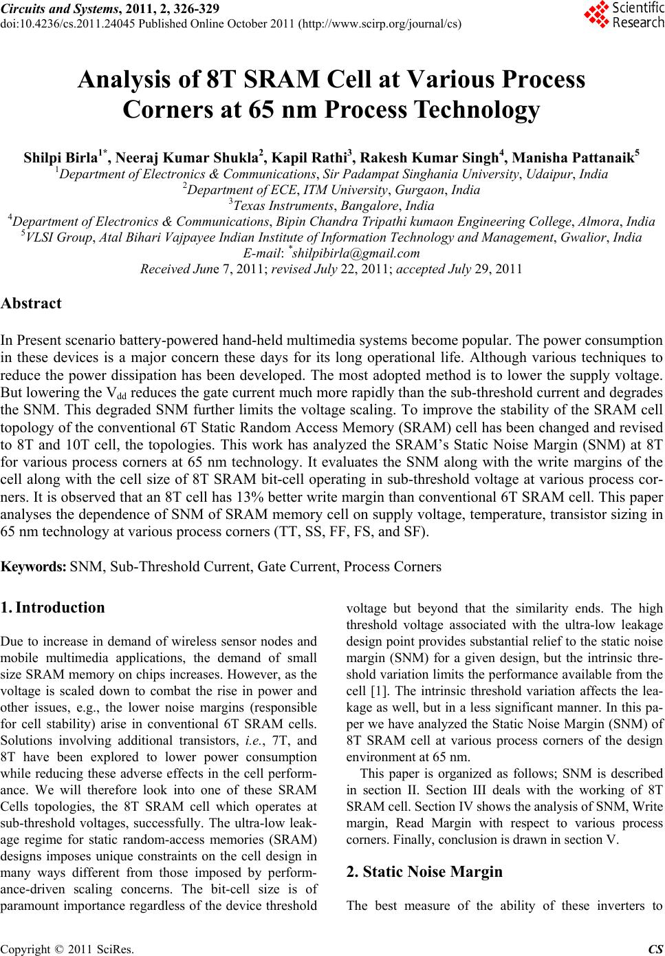
A simulation and analysis has been performed on the
static noise margin at 65 nm at various process corners.
The results shows that at SF corner the SNM is the
max imu m and a t FS co rn er the S NM is mini mum, Table
1. TT corner shows moderate value. As we measure the
SNM at varying temperature at 40˚C and 100˚C, we
found that as the temperature increases and the SNM
decreases. As the Vdd increases the SNM has also in-
creased but this increase in Vdd leads to increase in leak-
age current.
4.2. Analysis of Write Margin at Various Process
Corners
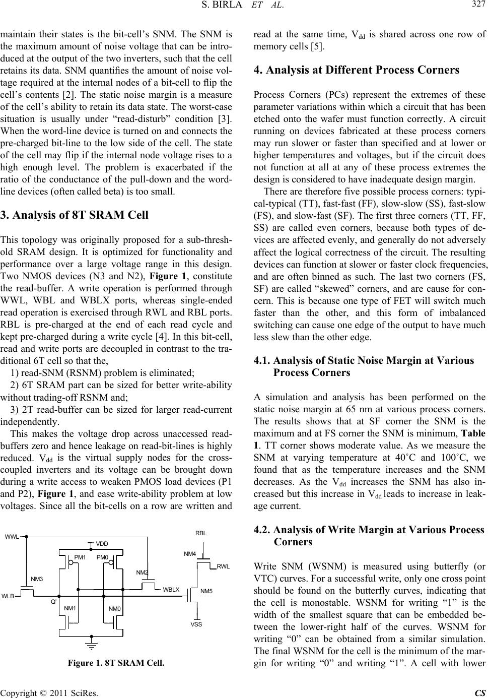
Write SNM (WSNM) is measured using butterfly (or
VTC) curves. For a successful write, only one cross point
should be found on the butterfly curves, indicating that
the cell is monostable. WSNM for writing “1” is the
width of the smallest square that can be embedded be-
tween the lower-right half of the curves. WSNM for
writing “0” can be obtained from a similar simulation.
The final WSNM for the cell is the minimum of the mar-
gin for writing “0” and writing “1”. A cell with lower
S. BIRLA ET AL.
Copyright © 2011 SciRes. CS
328
Table 1. SNM at various Vdd and PCs for 8T SRAM Bit-Cell at 65 nm.
SNM (V)
(TT Corner) SNM (V)
(SS Corner) SNM (V)
(FF Corner) SNM (V)
(FS Corner)
Vdd
(V) 100˚C 40˚C 100˚C 40˚C 100˚C 40˚C 100˚C 40˚C
1.2 0.207 0.192 0.232 0.242 0.142 0.157 0.117 0.137
1.1 0.187 0.202 0.217 0.227 0.137 0.152 0.112 0.132
1 0.177 0.187 0.202 0.207 0.132 0.147 0.107 0.122
0.9 0.162 0.172 0.182 0.187 0.127 0.137 0.096 0.107
0.8 0.147 0.152 0.162 0.167 0.117 0.127 0.081 0.086
0.7 0.127 0.132 0.137 0.142 0.107 0.117 0.061 0.066
0.6 0.107 0.112 0.117 0.117 0.091 0.096 0.041 0.046
0.5 0.086 0.067 0.091 0.096 0.076 0.081 0.021 0.026
0.4 0.066 0.066 0.071 0.071 0.057 0.061 0.004 0.009
0.3 0.041 0.041 0.046 0.046 0.041 0.011 failed failed
WSNM has poorer write-ability. The BL voltage can also
be used as a measure of write margin [6]. The 6T cell is
configured for a write “1” case. The voltage of BLB the
bit-line connected to the node holding “1” initially is
swept downward during simulation. The write margin is
defined as the BLB value at the point when Q and QB
flip, which we will call VBL. The lower that value is, the
harder it is to write the cell, implying a smaller write
margin. Fro m Figures 2 and 3, it can seen that as the Vdd
increases the write margin increases, this trend of in-
creasing write margin can be seen in each process corner.
As the temperature increases the write margin increases
too, as we can see that at 40˚C (Figure 2), the write mar-
gin at TT is 0.148 V and at 100˚C it is 0.167 V, (Figure
3), an increase in 0.19 V.
4.3. Analysis of Read Current at Various Process
Corners
In some sense, stability can be viewed from write ability
and read access time. The more stable the cell, the more
difficult it will be to write the cell into a different state. A
cell design with a narrower word-line device is more
stable, but as the current through such a device is smaller,
it will require more time to develop a signal of a given
magnitude on the bit-line. The rate at which the cell can
pull down the bit-line is limited by the series combina-
tion of the pull down device and the word-line device,
and is increased by increasing the conductance of either
or both devices [7]. The relative importance of the two
devices to the read current is a consequence of the details
of the device design and the operating conditions, and
may not be precisely equal. For minimum read delay the
widths of both devices should therefore be as wide as
possible. While SNM evaluate cell functionality, the cell
read current, “Iread” is a major component in designing
array access time.
Figure 2. Write margin at 40˚C measured at various proc-
ess corners.
Figure 3. Write margin at 100˚C measured at various proc-
ess corners.
The correct write operation requires that stored data be
overwritten by the access devices; however, the relative
S. BIRLA ET AL.
Copyright © 2011 SciRes. CS
329
device strengths necessary to ensure this cannot practi-
cally be guaranteed. Further, the increased sensitivity to
variation also results in extremely low worst case read-
current. The resulting effect on performance is drastic,
but, even more importantly; the effect on functionality
can be fatal, where the read-current can be exceeded by
the aggregate bit-line leakage-current. As shown in Fig-
ures 4 and 5, we can analyze, as the temperature in-
creases the read current decreases and it is the highest for
FF corner. So, increase in temperature degrades the read
current which degrades the stability.
5. Conclusions
Voltage scaling enables energy minimization and leak-
age power reduction in micro-power systems. However,
the design techniques and circuit peripherals are nece-
Figure 4. Read current at 40˚C measured at various process
corners.
Figure 5. Read current at 100˚C measured at various proc-
ss corners. e
ssary to overcome the process variations in the ultra-low
voltage regime. This work analyzed the SRAM Bit-cell’s
stability of the 8T cell at the 65 nm technology. The cell
size of the 8T cell is 0.525 µm2 and it is seen that as the
voltage decreases, the SNM decreases. The temperature
also affects the stability when it is at the higher side. On
the other side, if the supply voltage Vdd increased, it in-
creases the leakage and may lead in exceed in the read
current. To minimize the Vdd, other low-voltage tech-
niques may be used, so that the leakage can be mini-
mized with maximized stability. It is also observed that
the stability is the best with FF process corner and it has
intermediate stability at the TT process corner.
6. Acknowledgements
All the authors are grateful to their respective organiza-
tions.
7. References
[1] S. Birla, N. Kr. Shukla, M. Pattanaik and R. K. Singh,
“Device and Circuit Design Challenges for Low Leakage
SRAM for Ultra Low Power Applications,” Canadian
Journal on Electrical & Electronics Engineering, Vol. 1,
No. 7, 2010, pp. 156-167.
[2] B. H. Calhoun and A. P. Chandrakasan “Static Noise
Margin Variation for Sub-Threshold SRAM in 65 nm
CMOS,” IEEE Journal of Solid-State Circuits, Vol. 41,
No. 7, 2006, pp. 1673-1679.
doi:10.1109/JSSC.2006.873215
[3] Y. Chung and S.-H. Song, “Implementation of Low-
Voltage Static RAM with Enhanced Data Stability and
Circuit Speed,” Microelectronics Journal, Vol. 40, No. 6,
2009, pp. 944-951. doi:10.1016/j.mejo.2008.11.063
[4] N. Hiroki, S. Okumura, Y. Iguchi, et al., “Which Is the
Best Dual Port SRAM in 45 nm Process Technology? 8T,
10T Single End and 10T Differential,” IEEE Interna-
tional Conference on Integrated Circuit Design and Tech-
nology and Tutorial, Austin, 2-4 June 2008, pp. 55-58.
[5] B. H. Calhoun and A. P. Chandrakasan “A 256-kb 65-nm
Sub-Threshold SRAM Design for Ultra-Low-Voltage
Operation,” IEEE Journal of Solid-State Circuits, Vol. 42,
No. 3, 2007, pp. 680-688.
doi:10.1109/JSSC.2006.891726
[6] Koichi Takeda, et al., “A Read Static Noise Margin Free
SRAM Cell for Low Vdd and High Speed Applications,”
IEEE Journal of Solid-State Circuits, Vol. 41, No. 1,
2006, pp. 113-121. doi:10.1109/JSSC.2005.859030
[7] R. Keerthi and H. Chen, “Stability and Static Noise Mar-
gin Analysis of Low Power SRAM,” IEEE International
Instrumentation & Measurement Technology Conference,
Victoria, May 2008, pp. 1541-1544.