Journal of Biomedical Science and Engineering
Vol.07 No.11(2014), Article ID:50263,14 pages
10.4236/jbise.2014.711092
Designing Wireless Charger Circuit for Hearing Aids Using Radio Frequency Waves
Seyed Ataaldin Mahmoudi Nejad, Naser Safdarian*
Department of Biomedical Engineering, Dezful Branch, Islamic Azad University, Dezful, Iran
Email: atamahmoudinejad@gmail.com, *naser.safdarian@yahoo.com
Copyright © 2014 by authors and Scientific Research Publishing Inc.
This work is licensed under the Creative Commons Attribution International License (CC BY).
http://creativecommons.org/licenses/by/4.0/


Received 30 July 2014; revised 15 September 2014; accepted 25 September 2014
ABSTRACT
In this paper, an attempt has been made to produce a recipient system of wireless charge for a simple hearing aid so that electrical signal would be generated through detecting and receiving radio frequency waves (RF). The purpose of this design is to receive wireless charge for hearing aids and basically for any electronic device which is not required to a high energy for being setup. In this study, it has been demonstrated that as the amount of radio receiving energy increases, distance of receiver from antenna should be decreased; otherwise, either maximum amount of the receiving energy, or signal power density of the transmitter should be increased. Since it is impossible to be performed, it is decided to set up an energy receiving system constructed by rectenna and charge Circuit and to adjust their parameters to provide energy requirements for a device with low-power consumption. In this paper, different components of an energy receiving system from radio frequency band have been mentioned and a diagram block has been suggested. Subsequently, input impedance of designed antenna has been adjusted by provided relations. This impedance should be adjusted with the total impedance of regarded hearing aid Circuit by which the highest amount of received signal power is transferred to the battery of hearing aids. Received signal is converted to a dc voltage by rectifier diode. Finally, by applying a voltage regulator which has been designed using a common-collector amplifier not only the output voltage is kept constant, but the power is also strengthened. The battery of the hearing aids will be charged using the obtained power and voltage.
Keywords:
Radio Frequency Waves (RF), Rectenna, Spiral Antenna, Charge Circuit, Impedance Adjustment or Impedance Matching, Array Antenna, Regulator Circuit, Hearing-Aid Circuit

1. Introduction
Receiving energy from radio frequency is an idea whose time has come to be considered. In this paper, the technology has been introduced exclusively for receiving energy from the RF frequency band. Nowadays, there are more than 5 billion cell phones, 44,000 radio centers, thousands of television centers, and unlimited wireless home networks throughout the world. Therefore, the extensive sources of radio waves are the best idea for receiving safe and renewable energy.
Here is an overview of previous researches on the topic. Description of the Prior Art Recharging devices using an RF electromagnetic field radiated into free space has been described US Patent 6,127,799 entitled, “Method and Apparatus for Wireless Powering and Recharging”. This patent discloses a battery charging arrangement in which a rechargeable charge storage device is placed in an RF or microwave radiation field. In one aspect of the invention, a charge storage device is charged by exposing the charge storage device to an RF electromagnetic field radiated into free space. The charge storage device includes one or more antennae disposed on the device and adapted to receive the radiated RF electromagnetic field [1] . In this research, one or more rectifiers are connected to the antennae for rectifying the received RF electromagnetic field into a DC output current. The DC output current produced by the rectifier is used to charge the charge storage device. To efficiently couple the antenna array consisting of several antennas in small pieces which is in the form of multi-antenna or an antenna with frequented fractals and uniform placed side by side and whole antenna including sub-fractals that are antenna arrays to the radiation field, each of the antenna elements of the array preferably has a length of approx-
imately , wherein
  is the wavelength of the RF signal received by the antenna. It should be mentioned
that, as the number of arrays of the dipole antenna increases, the amount of power received from antenna signal also increases [1] .
In this regard, resonant antennas such as dipole antennas are more efficient for a given length of wire, but are restricted to narrow bandwidths [1] . Most present day users of antennas for communication purposes desire an antenna that can operate on multiple frequencies without requiring antenna tuning or special impedance matching circuits [1] . Patent 5,111,213 entitled, “Broadband Antenna” discloses a broadband HF antenna in which the entire length (height) of the antenna radiates radio frequency energy The insertion resistor is introduced at the top of the antenna or on the inside surface of the antenna radiating element. The radio frequency antenna current travels through the insertion resistor and continues for an appreciable electrical distance in a coaxial cable and/or other passive components, Thus, the invention provides greater usable electrical radiating element length for a given physical antenna length (height) [1] .
US Patent Application 10/624,051 by Mickle et al. entitled, “Energy Harvesting Circuits and Associated Methods” discloses an energy harvesting Circuit that has an inherently tuned antenna, with at least portions of the energy harvesting Circuit structured to provide regenerative feedback into the antenna to thereby establish an effective antenna area substantially greater than the physical area [1] .
Among problems in the previous studies, energy received by the suggested circuits can be considered which could not effectively be received by the frequency of operating antenna.
Some challenges debated in the previous research can be mentioned. Firstly, in order to receive energy from electromagnetic signals, it is important to use an antenna with specific features which is different from antennas used for communication purposes. In addition, the issue of antenna design is itself one of the debated challenges in the previous research. Another challenge which has been considered in the previous research is an efficient impedance matching Circuit by which RF energy would be received from a wide band of RF and is able to receive maximum of energy in the mentioned band. In this paper, an effort has been made to present scientific and reasonable methods to overcome these challenges, and to suggest a Circuit and an antenna in this regard. In this research, firstly, different components of a receiving energy system from radio frequency band were listed and the suggested diagram block was presented. Secondly, the performance method of each component was explained. Finally, output system was studied and analyzed and the results were reported.
In the present study, considering the previous research, examining their strengths and weaknesses and trying to overcome the shortcomings, we present our proposal. So, the present study is a scientific research in order to design and offer a wireless charging system and overall action plans for the implementation.
2. Methods and Materials
2.1. Calculation of Energy Amount of Radio Frequencies
The amount of RF energy available to receive a radio tower is calculated as Equation (1) [2] :
 (1)
(1)
 Represents signal power density which depends on power extracted from radio source
  and direct gain of antenna
  and also distance of antenna from receiver
 .
.
In order to maximize the amount of radio energy, receiver distance from antenna should be reduced; however, due to lack of this possibility in the present project, maximum amount of energy should be increased, because there is not any possibility for increasing signal power density of the transmitter. With regard of mentioned problems, the best way is to increase maximum amount of energy through the antenna. For this, designing antenna and impedance matching Circuit is required [3] [4] .
2.2. General Algorithm of Suggested Method
Before studying antenna and relevant impedance matching Circuit, general model of the device need to be presented to discuss its diagram block (Figure 1).
In the following, rectenna is studied as the primary part of the device. In addition, the relations between antenna and frequency bands are also investigated.
Rectenna consists of 3 main parts: Antenna, impedance matching Circuit, and correction Circuit which converts AC signal into DC signal. In this paper, a rectenna is presented for radio bandwidth. Moreover, it is preferred to use a spiral antenna, because this is a resonant dipole antenna which is capable for receiving a small amount of power. As it is going to be suggested for hearing aid, the antenna will be designed as low-volume and small as possible. Since it has a spiral fractal, this antenna has an acceptable gain in receiving RF frequency band with a low volume [5] . Figure 2 illustrates general schematic spiral-shaped of antenna.
The spiral part of the antenna is made of two identical arms which are placed with the proportion of 180 degrees from one another. Spiral arms might be demonstrated in the form of two curves which are placed with the proportion of 90 degrees from each other. Entire spiral antenna consists of rotating a single curve in 4 scales of 90 degrees relative to the primary source. The curve of spiral antenna is explained by the Equation (2) as follows:
 (2)
(2)
In this equation,  stands for starting distance in the angle of
  and “
and “ ” determines increase rate of radius “
 ” (ex: if the arms are rotated once and 4 times totally, “
 ” would be 4, since it is 4 times of primary rotation rate).
  and
and  shows respectively available angle and curve rotation rate (bent arms). External curve in
  angle and internal curve in
  angle have been adjusted (Figure 3) [7] .
For designing the antenna, the first step is calculation of impedance of the antenna based on the following equation:
 (3)
(3)
In this equation,  is the impedance rate,
  is the length of antenna, and
  indicates the amount of the desired signal wavelength. In order to calculate
 , speed of light is divided by desired operating frequency, which is AM band and average of 1 MHz frequency. Here, it is assumed that
 , and antenna length is L = 1 m; hence, the amount of impedance is 0.008 ohms
 , which is very small value, regarding equation 3. As a result, antenna impedance should be reached almost 75 to 80 ohms using a coil wrapped around a carbon coal so that antenna impedance would be equal to transmitter impedance which is approximately 75 ohms (for understanding the aspect check [7] - [9] ). After reaching the antenna input impedance to 80 ohms, it should be adjusted with the total impedance of hearing aid Circuit by which the highest amount of signal power would be received. Maximum of signal power will be calculated in the following. The importance of the antenna impedance is in transferring power from transmitter to antenna and from antenna to the environment. In order to transfer maximum of power, adjustment of impedance is necessary.

Figure 1. General diagram block of suggested design of wireless charge Circuit for hearing aid.

Figure 2. Spiral antenna [6] .

Figure 3. Spiral antenna and its design parameters [7] .
To design a suitable impedance matching Circuit for the suggested model, following equations are essential, which will be discussed. In general, in high frequency signals, suitable impedance adjustment between different classes should be existed for transferring maximum power. There is a condition for transferring maximum power from source to charge; impedances of both source and charge should be paired. Adjustment of impedance is performed both for ohm charges and mixed charges. Impedance adjustment is operated in RF using compact elements (inductors and capacitors). Usually, to increase total quality coefficient in adjustment of impedance, inductor or capacitor is placed in series with smaller resistance and parallel with larger resistance [2] (Figure 4).
Transfer power to the charge:
 (4)
(4)
Equation of  indicates condition of power maximum transfer from source to the charge. As a result, maximum power delivered to the charge is equal to:
 (5)
(5)
In equation above, for  it is assumed:
 (6)
(6)
According to the mentioned equations, delivered power maximum from antenna to the battery of hearing aid (charge) can be calculated. Before calculation, different types of impedance adjustment structures should be evaluated [2] (Figure 5).
In this paper, since the goal is to receive energy from the entire frequency spectrum, in additional to the antenna, all Circuit elements should be also considered as broadband or entire-range [5] ; hence, even impedance adjustment Circuit cannot be linear. As a result, non-linear elements should be used to receive energy from more frequency spectrum. In other words, variable inductor and capacitor or potentiometer should be used instead of resistor so that suggested impedance adjustment Circuit would have more guarantee and efficiency. Therefore, after designing Circuit and using a combination of design patterns of impedance adjustment Circuit, range of inductor and capacitor variations or resistors are calculated with regard of frequency band. Finally, non-linear and variable are used to final design of the Circuit.
In order to calculate change interval of inductor and capacitor values, it is essential to calculate inductor and capacitor values required for the beginning and end of frequency band using equations which will be discussed in the following. Afterward, by subtracting calculated amount for received signal frequency maximum from inductor value and for received signal minimum from capacitor value, change range rate of mentioned elements would be obtained and thereby the inductor and capacitor would be designed.
Generally, in adjusting two ohm impedances, assuming , firstly, a quality coefficient is defined according to Figure 6 and secondly, the values of
  and
and  are determined based on Equation (7). Finally, inductor and capacitor impedance values are specified according to their
  equations.
 (7)
(7)
Hence, according to , Figure 6 is obtained:
 (8)
(8)
 (9)
(9)
 (10)
(10)
For instance, here antenna impedance is 80 ohm, so . Moreover, impedance of a hearing aid model is 150 ohm, so
 . As a result:

Figure 4. Circuits and equations related to impedance adjustment [2] .

Figure 5. Different types of impedance adjustment structures using compact elements [2] .

Figure 6. Circuit and equations related to calculation of inductor and capacitor impedance [2] .
 (11)
(11)
The amount of inductor and capacitor was obtained regarding to the structure of impedance adjustment Circuit.
For example, equation below should be considered according to Figure 7 using adjustment Circuit:
 (12)
(12)
In addition, we know that adjustment Circuit plays as a filtering roll of unwanted frequency bands and adapts antenna with the frequency. It means that fractal antenna with the use of adjustment Circuit presents maximum efficiency for operating frequency of adjustment Circuit [2] . Moreover, an impedance adjustment Circuit with a high efficiency can be designed by using more suitable combinations of inductors and capacitors so that an acceptable voltage from received signal would be obtained by suggested rectenna. Since received signal has poor power at the micro-amps, the power and voltage are supplied for the batteries of the hearing-aid using multi- level clamping Circuit and in the following a class of common collector. Since there are different types of hearing-aid battery with the minimum hearing-aid voltage of about 1.7 volt and required power of 1 mA and low power amount as well, the power can be used as a low-consumption battery of a device such as hearing-aid based on the proposal. Another important point in designing rectenna is that to receive energy from entire frequency band, all parts of rectenna block should be broadband.
In one of the papers, a relatively ideal design was found for schematic rectenna block in which array antenna was embedded properly along with the other impedance adjustment Circuits and block correction Circuit of ac to dc signals (see Figure 8). Hence, in this paper, mentioned system has been presented and considered in the proposal [3] [4] .
Figure 9 is an invention made by H. Mickle, Harold Marlin, C. Capelli, and Christopher Swift which has been patented in America and its patent number is US 7,084,605 B2. Almost all the relevant blocks in this invention have been analyzed according to the research done [1] . In this paper, what is going to be studied is to evaluate output power of energy receiver Circuit from environmental signals in different frequency bands using different antennas. This is the first step in improving suggested system of antenna design and studying energy power spectrum density in different frequency bands. The second step is to design an impedance adjustment Circuit, which is efficient for desired frequency bandwidth. In addition to this, some suggestions would be presented for further research in this regard in conclusion section.

Figure 7. A sample of adjustment circuit.
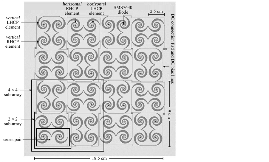
Figure 8. Layout of the 64-element array. Received RF power is rectified at each spiral locally and the combined dc power for all elements is extracted using two dc collection lines at the edges of the array [3] [4] .
According to the proposal, instead of final energy storage device, the battery of hearing-aid can be considered. By studying the paper, research team work results, which were successful in recording invention and setting up wireless energy receiving system from environment, can be inspired. This system can be also used in hearing-aid. As shown in the paper, relevant details of the blocks have not been explained; hence, it has been attempted to explain the blocks according to previous research and scientific and logical evidences. It is important to consider switch block as a manual key so that users themselves can turn it on or off as required. It acts as a relay and causes the battery of hearing-aid not to be charged constantly. Here, a summary of extracted results from the paper has been presented to give a proper view and analysis of proposal results.
According to conducted explanations and analysis and receiving energy and output from paper results and performed invention as well [1] , it can be concluded that there is not any necessity to have separation and demodulation for a specific frequency in receiving wireless energy and signal information. Rather, the aim is to increase output power of the suggested system. As a result, gaining signal energy component that is power spectrum of the signal at different frequencies and bandwidths as well as receiving it is the most important purpose so that it would be applied as a signal for a communication system such as suggested charge Circuit of signal energy. Therefore, system result can be an aggregate of electromagnetic signals of energy at different frequencies. Finally, receiving signal should be rectified and converted into DC electrical power using a broadband diode.
According to that invention [1] , to increase the efficiency of our proposed scheme, we can propose each array of spiral (helical) in Figure 8 as a helical antenna with three branches in Figure 10 or four branches in Figure 11. The antenna with four branches is more efficient than the antenna with three branches.
Figures 12(a)-(e) show suggested spiral antenna performance in similar physical paces [1] .
Basically, in this paper and suggested Circuit, energy has been detected by environmental signals and received

Figure 9. Performed invention diagram block which is a schematic description of an energy receiving system controlled by an adjustable system [1] .

Figure 10. Schematic and visual description of accomplished invention which is demonstrated configuration of three-branch antenna [1] .

Figure 11. Schematic and visual description of accomplished invention, which is demonstrated configuration of four-branch antenna [1] .

 (a) (b)
 (c) (d)
 (e)
(e)
Figure 12. Show suggested spiral antenna performance in similar physical paces [1] .
by rectenna block. It is also rectified by a broadband and low-consumption diode (preferably germanium) and converted into DC power (see Figure 13 and Figure 14).
Finally, voltage and power can be adjusted and stabilized using a regulator Circuit and converted into chargeable battery.

Figure 13. A schematic description of performed invention which contains three- branch antenna beside control Circuits, rectennas, and charge Circuits [1] .

Figure 14. A schematic description of performed invention which contains three-branch antenna along with DC receiving energy collector Circuit from antenna element, and it finally combines with rectenna block and electrical DC power output can be saved on energy storage device, such as a rechargeable battery [1] .
2.3. Voltage Regulator
Most electronic Circuits and electronic devices require power supplies to provide energy and system consumption power. Supplies or sources required are provided by urban power and converted into DC voltage in power supplies. Now, if power charge or power voltage is changed for any reason, will output voltage of power supplies remain stable? The answer to this question is “No”. It should be kept in mind that if charge power, input voltage of power supplies, or environmental temperature is changed, output voltage will be also changed [6] . This change of the voltage affects relevant devices such as laboratory equipment, computer Circuits, and industrial systems and causes errors in its performance. To avoid such errors, output voltage of power supplies should be remained stable. Voltage regulators are used to stabilize output voltage of power supplies. Voltage regulator prevents voltage changes of two charge poles and remains it stable.
2.3.1. Zener Voltage Regulator
Define Figure 15 shows suggested regulator Circuit [10] :

Figure 15. Zener voltage regulator [10] .
A Zener regulator has been suggested in Figure 15. As shown, output voltage of an unregulated power supply is entered into Zener regulator Circuit as voltage (rectenna block). As long as  is more than Zener voltage
 , power is connected in Zener Circuit and Zener diode is placed in fracture area. In this paper, any consumer connected to regulator output is called “charge”. Charge may be a computer, part of a TV Circuit, or an electronic device that the purpose of this paper is hearing-aid battery. Stable and smooth voltage of output regulator is transferred to the charge to activate it. In practice, all power supply designs are performed based on the charge features. Limitative resistance of
  prevent Zener power increase from exceeding maximum limit
 . In normal conditions, Zener diode acts as a battery; hence, the voltage of two charge poles remains stable. When output voltage of an unregulated power supply is not changed and as long as this voltage is more than Zener fracture voltage, Zener diode in fracture area would work and the voltage in the two resistance charge poles would remain stable. If output voltage amplitude of power supply is less than Zener fracture voltage, Zener diode will be driven out from Circuit, and unstable voltage of power supply will directly approach to the charge [10] . When using Zener diode, allowed power of Zener diode and its series resistance. In the following, voltage regulator Circuit with amplifier has been suggested since basic problem in this proposal is low power of rectenna class output [10] - [12] .
2.3.2. Voltage Regulator with Amplifier
Transistor can amplify power in common emitter and collector modes. If amplifying voltage is not required, common collector Circuit is the most suitable Circuit for amplifying power, because its power amplification coefficient and input resistance is high. A voltage regulator Circuit with common collector amplifier has been illustrated in Figure 16. In this Circuit, power transmitted from charge is equal to transistor emitter power which is . Therefore, charge power increases in comparison to Zener simple regulator in the Circuit. Moreover, output voltage decreases as much as
  than Zener two-pole voltages regarding to Kirchhoff's law in Zener diode ring and charge resistance, that is
  [10] - [12] .
Before discussing the last block which is hearing-aid battery presented as a chargeable battery in the paper, information related to hearing-aid and its different types are necessary to be explained.

Figure 16. Voltage regulator with common collector amplifier (power amplifier) [10] .
2.4. Hearing-Aid
Hearing-aid is an electronic device which works with the help of battery. It also amplifies voice to provide more connection. Hearing-aid receives voice through microphone and converts sound waves into electrical signals. The amplifier amplifies received sound signal and send it to ear via speakers [13] .
2.4.1. Different Types of Hearing-Aid
Hearing-aids are divided into three categories based on Circuit type [13] :
・ Analog;
・ Programmable;
・ Digital.
2.4.2. Analog Hearing-Aids
Analog hearing-aids convert sound waves into electrical signals. These electrical signals are sent to amplifier. Mentioned hearing-aids have audio settings and modulators; however there is only one program to be set up [13] .
2.4.3. Programmable Hearing-Aids
Analog hearing-aids which are set up through computer have the capability to set up more than one program. So in comparison with analog hearing-aid are more flexible [13] .
2.4.4. Digital Hearing-Aids
These groups of hearing-aids convert sound waves received into numerical codes before amplifying (as a computer). Digital hearing-aids are adjustable in different frequencies since numerical codes contain information such as modulation or loudness. Digital Circuits provide more possibility for an audiologist in terms of patient’s requirements and various environmental conditions [13] .
3. Results
Given the relatively useful and brief information, an optimal battery has been presented for the simple and low- consumption hearing-aid, which has been shown in Figure 17. According to information illustrated, battery power can be calculated, and battery discharge rate can be considered to obtain minimum of required energy for compensating and charging the battery (see Figure 18).
In Figure 19, the simple and low-consumption hearing-aid has been demonstrated. Providing energy for this simple hearing-aid rather than design or analysis of hearing-aid Circuit or development of its features has been the purpose of investigating battery charge and discharge.
As shown in Figure 20, input yellow signal with insignificant peak as millivolt (MV) has been amplified approximately 3 times. If low-consumption transistors are used instead of usual ones, consumption power hearing- aid will be also reduced in turn [6] .
According to Figure 9, at first the signal power receiving through antenna proposed (Figure 8) and then transferred to the Circuit impedance matching to maximize the signal to be transmitted rectenna blocks. In rec- tenna blocks, AC to DC conversion signals and then output of this block went to the dc voltage regulator with

Figure 17. Information of an optimal battery for suggested hearing-aid.

Figure 18. Discharge battery in terms of hour.

Figure 19. Simple hearing-aid Circuit (in this Circuit, low-consumption germanium transistors can be used instead of BC549 and BC107 to reduce power consumption of hearing-aid).

Figure 20. The output of the simple hearing-aid circuit.
current amplifiers. The gulator block is used to control the system output, because in environments with highdensity, signal input in the antenna was increased, which consequently increases the output of system. So in order to supply 1.5 volts with 1 mA current for a low power hearing-aid should take control of the output.
According to the invention [1] , in Figure 12 (part of “a” to “e”) is that for a spiral helical antenna can be concluded that in the proposed method, by use from the proposed antenna in Figure 8, it can be the receive power will be multiplied. Consequently, with regard to the implementation of all aspects of the proposed method, witness system will be more efficient than the existing systems.
4. Conclusions
In this paper, an attempt has been done to simulate the idea of wireless charge Circuit design for hearing-aid as far as possible according to evidences and scientific calculations and present a scheme for implementing such a system. According to the explanations given above, power maximum can be transferred into hearing-aid battery (charge) by designing an impedance adjustment Circuit for adjusting antenna impedance with the total board impedance of a hearing-aid. Total charge board block will be the same as Figure 1, whose components were studied at different stages respectively, regarding proposals. We hope that this research is a step towards fulfilling this idea and a foundation for the future research. Since similar inventions have been patented, this proposal is not far-fetched and impossible. It can specially be practical for a very low-consumption device such as hearing-aid.
Basically, the most important challenge of the research is not to show that suggested system output is suitable for hearing-aid charge because even if the suggested system output is insignificant it is still useful and leads to longevity of hearing-aid battery as it is suggested for hearing-aid battery and assumed to be a chargeable battery. Therefore, capacitor discharge time will be longer and the user will not need much time for replacing or recharging battery.
Indeed, main challenge of the systematic design and the analysis for achieving the goal has been wireless charge of hearing-aid chargeable battery. Despite the limitations, the present paper has finally been able to cover weaknesses and previous research challenges partially. However, the implement of the suggested scheme has not been solved because of restrictions. In the future, more research should be done in the area of impedance adjustment Circuit optimization, development of device quality and usage of high electronic technology to achieve better results. In addition, antenna’s material should be considered so that if a specific alloy is using, whether it would have better power or not. Another issue is the use of low-power consumption components and the whole band which is important. Finally, the last suggestion is to use smart impedance adjustment Circuit with microcontroller for locking system on particular frequencies with higher signal power spectrum. At the end, we hope this research can be a step towards better future researches and open a new path for the implementation of the suggested scheme.
Acknowledgements
I would like to express my special thanks of gratitude to the dear guide “Naser Safdarian” who gave me support and supervisor to do this paper. Also, I would like to express my special thanks of gratitude to the translator Dr. Narges Naghibirokni who translated this paper into English language. We have tried to increase the quality of the present content as much as possible so that the audience can easily understand and analyze the origin of the suggested scheme. We hope that readers and critics of the paper can reveal strengths and weaknesses points of the research in order to improve it. With special thanks from Dezful Branch, Islamic Azad University, Dezful, Iran, this research was supported by this university. Lastly, we also hope that this paper can be considered by professors, students, engineers, scholars, and other readers.
Cite this paper
Seyed Ataaldin MahmoudiNejad,NaserSafdarian, (2014) Designing Wireless Charger Circuit for Hearing Aids Using Radio Frequency Waves. Journal of Biomedical Science and Engineering,07,948-962. doi: 10.4236/jbise.2014.711092
References
- 1. Mickle, M.H., Capelli, C.C. and Swift, H. (2006) University of Pittsburghs Pmsburgh, Energy Harvesting Circuit. Patent No. US 7,084,605 B2.
- 2. Toofan, S. (2009) Telecommunication Booklet. Zanjan University, Zanjan.
- 3. Lo, E., Truong, H. and Elnatan, L. (2005) Alvin Mar, Ha Nguyen, Wireless Battery Charger. Final Report.
- 4. Hagerty, J.A., Helmbrecht, F.B., McCalpin, W.H., Zane, R. and Popovic, Z.B. (2004) Recycling Ambient Microwave Energy with Broad-Band Rectenna Arrays. IEEE Transactions on Microwave Theory and Techniques, 52, 1014-1024.
- 5. Rumsey, V.H. (1957) Frequency Independent Antennas. IRE National Convention Record, 5, 114-118.
- 6. Yusef Zadeh, N., Jalali, M. and Pilehvari, M. (2006) Fractals and Their Application in Antenna Design, Student Conference on Electrical Engineering, Iran.
- 7. Mushiake, Y. (1992) Self-Complementary Antennas. IEEE Transactions on Antennas and Propagation, 34, 23-29.
http://dx.doi.org/10.1109/74.180638 - 8. Dyson, J.D. (1959) The Equiangular Spiral Antenna. IRE Transactions on Antennas and Propagation, 7, 181-187.
http://dx.doi.org/10.1109/TAP.1959.1144653 - 9. Thaysen, J., Jakobsen, K.B. and Appel-Hansen, J. (2006) A Logarithmic Spiral Antenna for 0.4 to 3.8 GHz. Applied Microwave & Wireless, 13, 32-45.
- 10. Samooti, S.M., Reza, Z.Y., Nasiri Savadkuhi, SH. and Shabani, M. (2013) Telecommunication and Radio Principles. Textbook Publishing Company of Iran, Tehran.
- 11. Ali, M.E.S. (2001) Electronic 1 and 2 Books. 5th Edition, Publication of Shykhbhayy.
- 12. Rezazadeh, Y., Nasri, GH.H. and Nazarian, F. (2010) Public Electronic. Textbook Publishing Company of Iran, Tehran.
- 13. Khanbaba, S. (2012) Hearing Aid. Final Report, Islamic Azad University of Dezful, Dezful.
NOTES

*Corresponding author.