Materials Sciences and Applications
Vol.4 No.11(2013), Article ID:39746,6 pages DOI:10.4236/msa.2013.411089
Electrodeposition and Characterization of Cu(In, Al)Se2 for Applications in Thin Film Tandem Solar Cells
![]()
1Sciences Faculty, Mohamed Boudiaf University, M’sila, Algeria; 2Thin Films and Interfaces Laboratory, Department of Physics, Mentouri University, Constantine, Algeria; 3Sciences and Technologies Faculty, Ziane Achour University, Djelfa, Algeria.
Email: *a_bouraiou@yahoo.fr
Copyright © 2013 Omar Meglali et al. This is an open access article distributed under the Creative Commons Attribution License, which permits unrestricted use, distribution, and reproduction in any medium, provided the original work is properly cited.
Received September 20th, 2012; revised October 22nd, 2013; accepted November 9th, 2013
Keywords: Electrodeposition; Cu(In, Al)Se2; Thin Film
ABSTRACT
Cu(In, Al)Se2 thin films were prepared by electrodeposition from the aqueous solution consisting of CuCl2, InCl3, AlCl3 and SeO2 onto ITO coated glass substrates. The as-deposited films were annealed under vacuum for 30 min at temperature ranging between 200˚C and 400˚C. The structural, composition, morphology, optical band gap and electrical resistivity of elaborated thin films were studied, respectively using x-ray diffraction, energy dispersive analysis of x-ray, scanning electron microscopy, UV spectrophotometer and four-point probe method. The lattice constant and structural parameters viz. crystallite size, dislocation density and strain of the films were also calculated. After vacuum annealing, x-ray diffraction results revealed that all films were polycrystalline in nature and exhibit chalcopyrite structure with (112) as preferred orientation. The film annealed at 350˚C showed the coexistence of CIASe and InSe phases. The average crystallite size increases linearly with annealing temperature, reaching a maximum value for 350˚C. The films show a direct allowed band gap which increases from 1.59 to 1.78 eV with annealing temperature. We have also found that the electrical resistivity of films is controlled by the carrier concentration rather than by their mobility.
1. Introduction
One of the main challenges in photovoltaic research is the development of lower cost and higher conversion efficiency devices. This primary objective can be achieved by using tandem solar cell structures. For the thin film tandem cell, the top cell requires a wide band gap absorber layer with optical band gap in the range 1.7 - 1.9 eV whereas the bottom cell requires an absorber layer with a band gap around 1.1 eV [1]. Fabrication of thin film tandem cell gets relatively simplified if the desired band gap semiconductor absorber layers for the top and bottom cells can be obtained from a single ternary or quaternary alloy system by varying the alloy composition suitably [1].
Cu(In, Al)Se2, abbreviated as CIASe, is considered as an quaternary interesting absorber material for the wide band gap cell in the thin film tandem structures, because it requires smaller relative alloy concentration than gallium (Cu(In, Ga)Se2) or sulphur (CuIn(S, Se)2) alloys to achieve comparable band gap. Furthermore, the aluminum is a much cheaper and abundant material [2]. The optical band gap of Cu(In1−xAlx)Se2 semiconductor can be controlled from 1 eV (for x = 0) to 2.7 eV (for x = 1) by the partial replacement of indium by aluminum [3,4]. The conversion efficiency has already exceeded 16.9% using CIASe material as absorber layer in solar cell [5]. These progresses open up new perspectives.
The CIASe thin films have been prepared by various methods such as chemical vapor transport [6], evaporation [1,7], selenization of evaporated precursors [8] chemical bath deposition [1], pulsed laser deposition [9], electrodeposition [10], etc. Amongst them, electrodeposition is an appealing technique that offers low-cost equipment, high deposition speed and possibility of large-area polycrystalline films deposition. In the present work, Cu(In, Al)Se2 films have been deposited on the indium tin oxide (ITO) coated glass substrate by one step electrodeposition process using two electrodes system. After vacuum annealing of the as-deposited samples, they have been characterized by using XRD, SEM, optical absorption and electrical resistivity. The relationship between the properties of the Cu(In, Al)Se2 films and the annealing temperature is also studied.
2. Experimental
In the present work, electrochemical experiments were carried out in a simple two-electrode cell configuration with a indium tin oxide (ITO) coated glass substrate as a working electrode (area 5 mm × 15 mm), and a palatine sheet as the counter electrode. The electrode position bath containing 10 mM CuCl2, 20 mM InCl3, 20 mM AlCl3 and 20 mM SeO2 dissolved in de-ionized water. The pH of the solution was adjusted to 2.6. Deposition was carried out at a room temperature, without stirring the solution. The as-deposited films were annealed under vacuum for 30 min at temperature ranging between 200˚C and 400˚C.
The crystalline structure of the resulting films was analyzed by means of x-ray diffractometer using CuKα radiation of wavelength λ = 1.5418 Å. Since no standard files are available for CIASe material, standard file of CuInSe2 was used to identify Cu(In, Al)Se2 elaborated films. The crystallite size Cs, was estimated from the full width at half maximum (FWHM) of the diffraction peak by using Scherr’s formula [11].
The surface morphology of the films was investigated using a scanning electron microscope (SEM). The optical transmittance of the films was recorded using UV-VisNIR spectrophotometer (Shimadzu UV-3101) at room temperature in the wavelength range of 350 - 1500 nm in steps of 2 nm. An identical ITO coated glass substrate was used as reference for recording the optical absorption spectra.
The thicknesses of the films were measured by means of a DEKTAK 3030 surface profile system. Electrical resistivity of the films was determined using four point probe method.
3. Results and Discussion
The x-ray diffraction pattern of the as-deposited film, before annealing, is shown in Figure 1. The XRD spectra appear the peaks correspond to the most intense peaks of ITO phase [12]. It is noted that before annealing we have observed only the XRD patterns related to the ITO phase. This indicates that the as deposited films are amorphous in nature or are composed with micro crystallite that cannot be detected.
The EDAX pattern for the as deposited films is given in Figure 2. The spectrum shows the typical emission lines of copper (CuL), indium (InL), aluminum (AlK) and selenium (SeL) elements in the investigated energy range. On the other hand, the appearance of silicon (SiK), oxygen (OK) and tin (SnL) peaks comes mainly from the
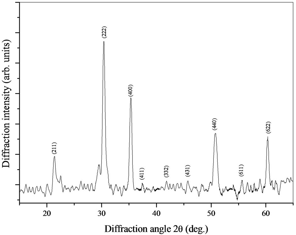
Figure 1. x-ray diffraction pattern of the as deposited thin film (before annealing).
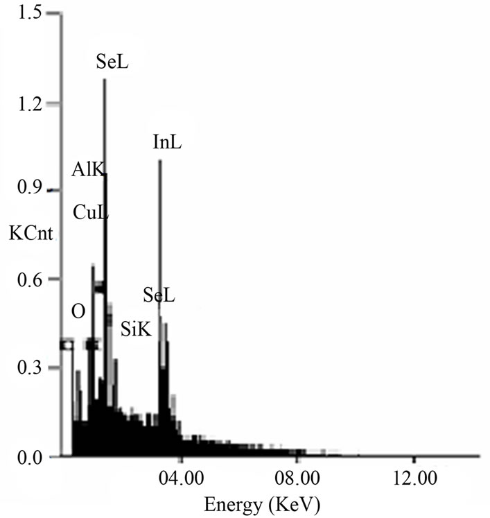
Figure 2. EDAX pattern of the as deposited film.
ITO coated glass substrate.
The x-ray diffraction patterns of the elaborated thin films, after annealing at different temperature are shown in Figures 3(a)-(d). All specimens are composed of polycrystalline CIASe and ITO phases, and no distinct peaks particular to CuInSe2 and CuAlSe2 are detected. Thereafter, the annealing results in changing CIASe films from amorphous to polycrystalline structure.
The XRD spectra appear the peaks located at 2θ ≈ 26.78˚ and 45.19˚. The present XRD pattern is most satisfactorily indexed on the basis of the chalcopyrite structure of CuInSe2 phase. The last peaks are the three most intense peaks for CIASe phase in its chalcopyrite structure [13], they correspond respectively to the (112) and (204)/(220) planes. The presences of these most intense reflections confirm the chalcopyrite structure of CIASe material.
Figure 4 shows the XRD patterns of the CIASe films near (112) diffraction peak. As can be seen from this
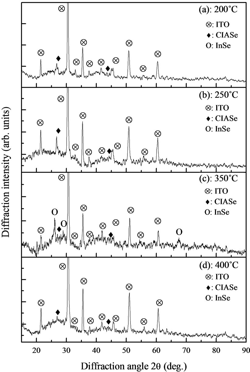
Figure 3. x-ray diffraction patterns of Cu(In, Al)Se2 films annealed at different temperature, (a) 200˚C; (b) 250˚C; (c) 350˚C; and (d) 400˚C. Symbols Ä, ¨, O indicated ITO, CIASe and InSe phases.
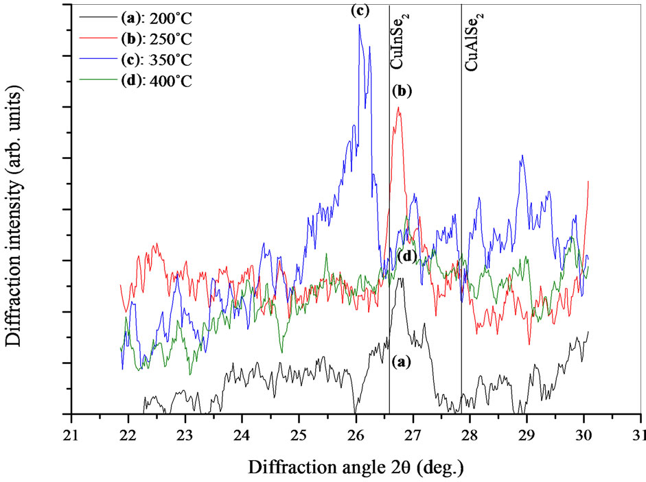
Figure 4. XRD scans reflecting only a section of the scan 22˚ to 30˚ for CIASe films, the vertical solid lines indicated respectively the position of (112) peak for CuInSe2 and CuAlSe2 materials.
figure, the position of (112) peak lies between that of CuInSe2 and CuAlSe2. The shift of (112) peak towards higher angles is due to incorporation of aluminum into chalcopyrite lattice. On the other hand, in addition to the CIASe reflection peaks, the film annealed at 350˚C exhibited some additional peaks situated at 2θ ≈ 26.03˚, 29.11˚ and 67.24˚ (Figures 3(d) and 4(d)), these peaks are attributed to InSe binary phase [14]. The appearance of InSe as secondary phase with the main Cu(In, Al)Se2 phase indicating an In-rich film.
The intensity of (112) peak as a function of the annealing temperature is shown in Figure 5. The intensity of (112) peak firstly shows an increasing tendency, reaching a maximum value for the film annealed at 250˚C then it decreases with annealing temperature. As announced above, this phenomenon can be related to the formation of InSe secondary phase which may hinder the growth of CIASe2 phase.
The average crystallite size, Cs of the films was calculated from the broadening of the x-ray peak using the well known Scherrer’s equation [11]
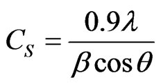 (1)
(1)
In which, l is the wavelength of the x-radiation, β is the full width at half maximum (FWHM) in radians of the main peak of the XRD spectrum corrected for instrumental broadening, and 2θ is the diffraction angle. Here, the Cs values, calculated from the (112) reflection of the chalcopyrite CIASe phase. The obtained results versus the annealing temperature are reported in Figure 6. We noted that, the average crystallite size increase linearly with annealing temperature, reaching a maximum value for 350˚C and then shows a decreasing tendency with annealing temperature from 350˚C to 400˚C.
The degree of preferential orientation in the films RI, was estimated from the XRD pattern as the ratio between the peak intensity of the most intensive (112) peak and the sum of intensities of all peaks [15]. It is found that the intensity ratio, RI, is ranged between 0.6 and 0.7; this shows the high degree of preferred orientation towards (112) direction for all deposited films. The obtained values are in the same range than that for CuInSe2 reported elsewhere [16].
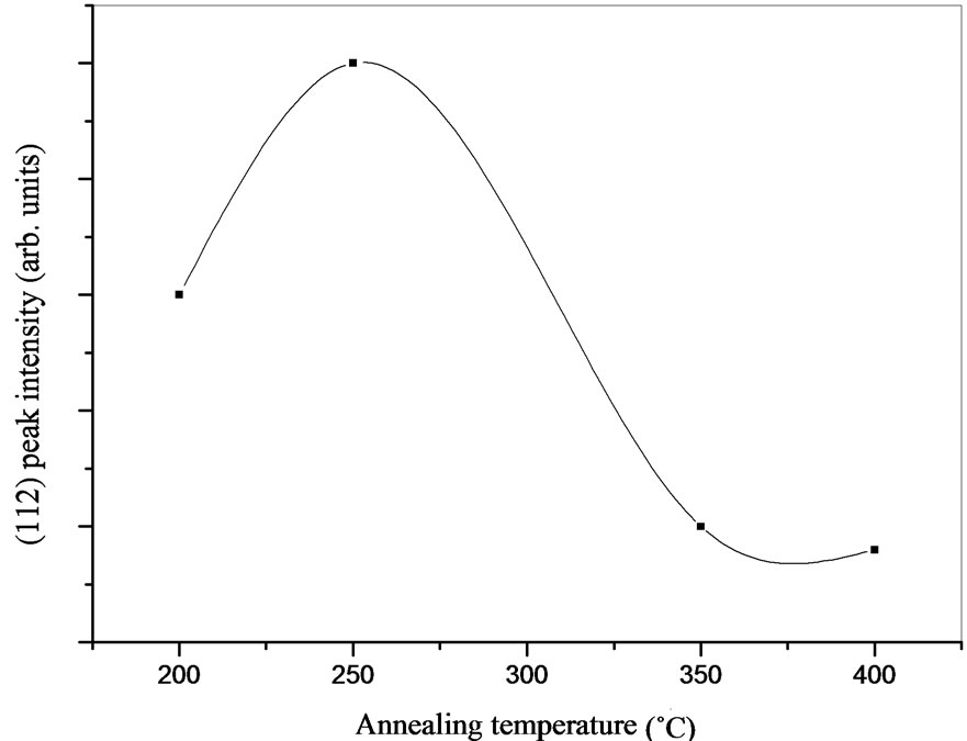
Figure 5. Variation of (112) peak intensity as a function of annealing temperature.
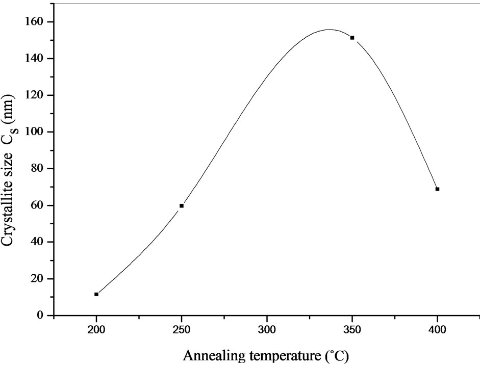
Figure 6. Variation of crystallite size versus annealing temperature.
The lattice constants (a and c), the dislocation density δ and the strain є in the films were calculated using the same scheme as described in ref. [17]; the obtained results are depicted in Table 1. The obtained values of the lattice constants are in good agreement with the results published in the literature. The lattice parameters of CuIn0.3Al0.7Se2 were reported by Bharath Kumar Reddy et al. [1] like a = 0.572 nm and c = 1.128 nm, and they were reported by Sugiyama et al. [18] a = 5.73 Å and c = 11.40 Å for CuIn0.74Al0.26Se2 films.
The morphology of the resulted films for different annealing temperature is shown in Figures 7(a)-(d). The SEM images point out that the annealing temperature has a marked influence on the morphology films. The image of the film annealed at 200˚C shows a smooth and good uniform morphology without visible pores. However, the films annealed at 250˚C and 350˚C (Figures 7(b) and (c)) are characterized by the presence respectively of a more irregular structure and relatively large spherical grain embedded on the surface of the compact structure. From Figure 7(d), it was observed that the film annealed at 400˚C is smooth, homogenous and densely packed.
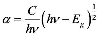
It is well known that CIASe material is a direct band gap semiconductor [19,20]. For direct band gap semiconductor, the optical band gap was deduced from the linear plot of the square of the absorption coefficient 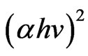 (Figures 8(a)-(d)) versus the photon energy (hν) near the band edge using the following relationship.
 (2)
(2)
Here, C, h, and υ represent a constant depending on the transition nature, Plank’s constant and frequency of the incident radiation.
The absorption coefficient α in the region of the fundamental absorption could be evaluated from the mea-
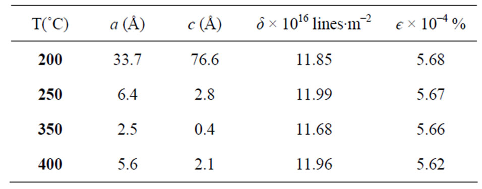
Table 1. The structural characteristics of CIASe films annealed at different temperature; a and c the lattice constants, δ the dislocation density and e the strain.
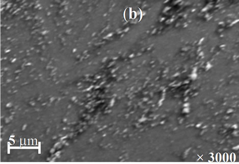
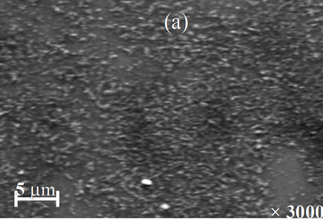
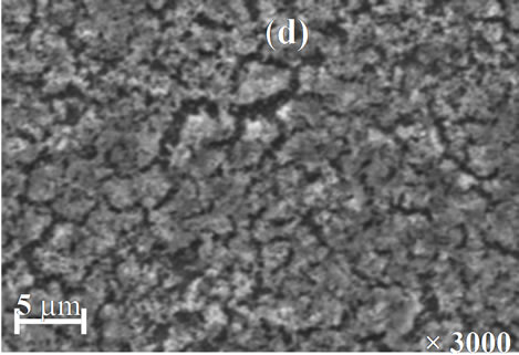
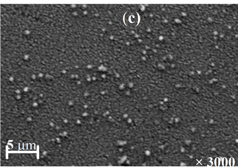
Figure 7. SEM images of Cu(In, Al)Se2 thin films annealed at (a) 200˚C; (b) 250˚C; (c) 350˚C; and (d) 400˚C.
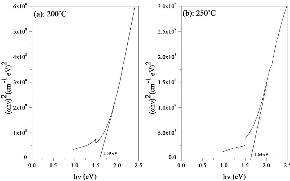
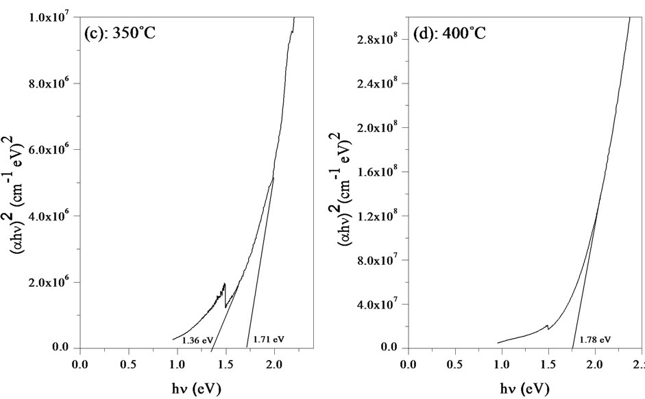
Figure 8. Dependence of the parameter on radiation energy (hν) related to annealing temperature (a) 200˚C; (b) 250˚C; (c) 350˚C; and (d) 400˚C.
surements of transmittance T and film thickness d using the relation:
 (3)
(3)
On the other hand, at low absorption levels, the absorption coefficient is described by the Urbach formula. The inverse of the slope from plot of ln(α) versus hυ gives the value of Urbach energy E00 [21]. The average thickness of the films was in the around of 1 µm.
The band gap energy Eg and the Urbach energy E00 versus the annealing temperature are shown in Figure 9. As can be seen, the variation of the band gap energy is opposite to the Urbach energy, similar observations have been reported by earlier workers [22].
The decrease of the Urbach energy is attributed to the decrease of the degree of structural disorder upon annealing of the films [23]. On the other hand, the band gap energy is an increasing function with annealing temperature and it ranging between 1.59 - 1.78 eV.
Two different slopes were observed in the Figure 8(c) indicating that two different optical transitions occur for this film. The optical band gaps value due to the additional transition in the case of this later film is found to 1.36 eV. As the optical band gap of InSe reported by De Blasi et al. was 1.32 eV [24] and according to the above XRD analysis which confirmed the mixed phases (CIASe and InSe) in the film annealed at 350˚C, this additional optical transition is attributed to InSe phase.
The obtained values are in good agreement with the results published in the literature. Dhananjay et al. [7], reported the band gaps of Ea = 1.51 and 1.73 eV respectively for CuIn0.5Al0.5Se2 and CuIn0.35Al0.65Se2.
Figure 10 shows the electrical resistivity measurements of the CIASe films as a function of annealing temperature. Films exhibited a range of resistivity varying from (4.12 ± 0.02) × 10−2 to (1.66 ± 0.18) Ωcm. The films annealed at 200˚C and 250˚C had low electrical resistivity, this can be traced back to the remaining of metallic layers that have note completely reacted during annealing and which cannot detected by XRD investigation [19]. On the author hand, we found that the pace of the electrical resistivity according to the annealing temperature is similar to that of the crystallite size, thus we inferred that the films resistivity is controlled by the carrier concentration rather than by their mobility. The obtained data are in good agreement with the values reported by earlier workers [25].
4. Conclusions
We have grown Cu(In, Al)Se2 thin films onto ITO coated glass substrate using a one-step electrodeposition process. We have found that the structural, morphological, optical and electrical resistivity of CIASe films is greatly in-
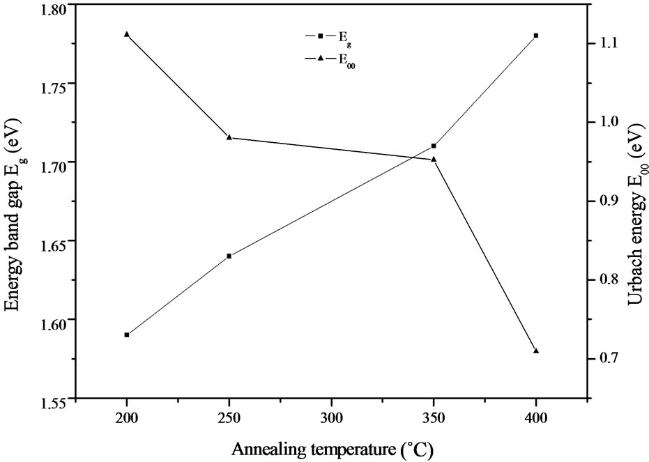
Figure 9. Variation of the band gap energy Eg and the Urbach energy E00 versus annealing temperature.
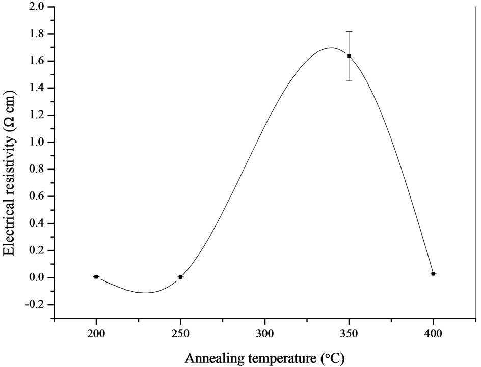
Figure 10. A plot of the electrical resistivity of CIASe films versus annealing temperature.
fluenced by the annealing temperature. The presence of Cu, In, Al and Se in the deposited film was confirmed by EDAX analysis. Polycrystalline CIASe thin films crystallizing in the chalcopyrite structure with the preferential orientation in the (112) plane were obtained. The film annealed at 350˚C showed with the main CIASe chalcopyrite phase and the InSe as secondary phase. The average crystallite size increases linearly with annealing temperature reaching a maximum value for 350˚C. The band gap energy of films is found to increase from 1.59 to 1.78 eV with annealing temperature.
The results derived from the present study suggest that the elaborated CIASe films can be useful as a top absorber layer in tandem solar cells.
REFERENCES
- Y. B. K. Reddy and V. S. Raja, “Preparation and Characterization of CuIn0.3Al0.7Se2 Thin Films for Tandem Solar Cells,” Solar Energy Material and Solar Cells, Vol. 90, No. 11, 2006, pp. 1656-1665. doi:10.1016/j.solmat.2005.09.002
- B. Kavitha and M. Dhanam, “In and Al Composition in Na-no-Cu(InAl)Se2 Thin Films from XRD and Transmittance Spectra,” Materials Science and Engineering B, Vol. 140, No. 1-2, 2007, pp. 59-63. doi:10.1016/j.mseb.2007.03.011
- T. Hayashi, T. Minemoto, G. Zoppi, I. Forbes, K. Tanaka, S. Yamada, T. Araki and H. Takakura, “Effect of Composition Gradient in Cu(In,Al)Se2 Solar Cells,” Solar Energy Materials and Solar Cells, Vol. 93, No. 6-7, 2009, pp. 922-925. doi:10.1016/j.solmat.2008.11.007
- D. C. Perng, J. W. Chen and C. J. Wu, “Formation of CuInAlSe2with Double Graded Band Gap Using Mo(Al) Back Contact,” Solar Energy Materials and Solar Cells, Vol. 95, No. 1, 2011, pp. 257-260. doi:10.1016/j.solmat.2010.04.046
- S. Marsillac, P. D. Paulson, M. W. Haimbodi, R. W. Birkmire and W. N. Shafarman, “High-Efficiency Solar Cells Based on Cu(InAl)Se2 Thin Films,” Applied Physics Letters, Vol. 81, No. 7, 2002, pp. 1350-1352. doi:10.1063/1.1499990
- N. Kuroishi, K. Mochizuki and K. Kimoto, “Surface Oxidation of CVT-Grown CuAlSe2,” Materials Letters, Vol. 57, No. 13-14, 2003, pp. 1949-1954. doi:10.1016/S0167-577X(02)01110-2
- Dhananjay, J. Nagaraju and S. B. Krupanidhi, “Structural and Optical Properties of CuIn1−xAlxSe2 Thin Films Prepared by Four-Source Elemental Evaporation,” Solid State Communications Vol. 127, No. 3, 2003, pp. 243- 246. doi:10.1016/S0038-1098(03)00389-2
- S. Martin and C. Guillen, “Characterization of Chalcopyrite Cu(In,Al)Se2 Thin Films Grown by Selenization of Evaporated Precursors,” Energy Procedia, Vol. 10, No. 1, 2011, pp. 182-186. doi:10.1016/j.egypro.2011.10.174
- K. H. Kim and Fianti, “Growth of Single-Phase CuInAlSe2 Thin Films by Using Pulsed Laser Deposition and Selenization,” Journal of the Korean Physical Society, Vol. 60, No. 12, 2012, pp. 2001-2006. doi:10.3938/jkps.60.2001
- D. Prasher, R. Sharma, A. Sharma and P. Rajaram, “CuIn1−XAlXSe2 Thin Films Grown By Electrodeposition,” Proceedings of the 55th dae Solid State Physics Symposium, Manipal, 26-30 December 2010, pp. 597-598. doi: 10.1063/1.3605999
- L. I. Malssel and R. Glang, “Handbook of Thin Film Technology,” McGraw Hill Book Company, New York, 1970.
- International Center for Diffraction Data, ICDD, PDF2 Database, File Number 76-0152 for In2O3.
- International Center for Diffraction Data, ICDD, PDF2 Database, File Number 40-1487 for CuInSe2.
- International Center for Diffraction Data, ICDD, PDF2 Database, File Number 73-0609 for InSe.
- J. Muller, J. Nowoczin and H. Schmitt, “Composition, Structure and Optical Properties of Sputtered Thin Films of CuInSe2,” Thin Solid Films, Vol. 496, No. 2, 2006, pp. 364-370. doi:10.1016/j.tsf.2005.09.077
- A. Bouraiou, M. S. Aida, E. Tomasella and N. Attaf, “ITO Substrat Resistivity Effect on the Properties of CuInSe2 Deposited Using Two-Electrode System,” Journal of Material Science, Vol. 44, No. 5, 2009, pp. 1241-1244. doi:10.1007/s10853-009-3252-y
- M. Dhanam, P. K. Manoj and R. R. Prabhu, “High-Temperature Conductivity in Chemical Bath Deposited Copper Selenide Thin Films,” Journal of Cristal Growth, Vol. 280, No. 3-4, 2005, pp. 425-435. doi:10.1016/j.jcrysgro.2005.01.111
- M. Sugiyama, A. Umezawa, T. Yasuniwa , A. Miyama, H. Nakanishi and S. F. Chichibu, “Growth of Single-Phase Cu(In,Al)Se2 Photoabsorbing Films by Selenization Using Diethylselenide,” Thin Solid Films, Vol. 517, No. 7, 2009, pp. 2175-2177. doi: 10.1016/j.tsf.2008.10.083
- E. Halgand, J. C. Bernède, S. Marsillac and J. Kessler, “Physico-Chemical Characterisation of Cu(In,Al)Se2 Thin Film for Solar Cells Obtained by a Selenisation Process,” Proceedings of Symposium O on Thin Film Chalcogenide Photovoltaic Materials, EMRS 2004 Conference, Strasbourg, 24-28 May 2004, pp. 443-446. doi: 10.1016/j.tsf.2004.11.039
- J. Lopez-Garcia, C. Maffiotte and C. Guillen, “WideBandgap CuInx-1AlxSe2 Thin Films Deposited on Transparente Conducting Oxides,” Solar Energy Materials and Solar Cells, Vol. 94, No. 7, 2010, pp. 1263-1269. doi:10.1016/j.solmat.2010.03.022
- F. Urbach, “The Long-Wavelength Edge of Photographic Sensitivity and of the Electronic Absorption of Solids,” Physical Review, Vol. 92, No. 5, 1953, p. 1324. doi:10.1103/PhysRev.92.1324
- H. Moualkia, S. Hariech, M. S. Aida, N. Attaf and L. Laifa, “Growth and Physical Properties of CdS Thin Films Prepared by Chemical Bath Deposition,” Journal of physics D: Applied Physics, Vol. 42, No. 13, 2009, Article ID: 135404. doi:10.1088/0022-3727/42/13/135404
- B. Pejova, “The Urbach—Martienssen Absorption Tails in the Optical Spectra of Semiconducting Variable-Sized Zinc Selenide and Cadmium Selenide Quantum Dots in Thin Film Form,” Materials Chemistry and Physics, Vol. 119, No. 3, 2010, pp. 367-376. doi: 10.1016/j.matchemphys.2009.08.064
- C. de Blasi, G. Micocci, S. Mongelli and A. Tepore, “Large InSe Single Crystals Grown From Stoichiometric and Non-Stoichiometric Melts,” Journal of Cristal Growth, Vol. 57, No. 3, 1982, pp. 482-486. doi:10.1016/0022-0248(82)90062-8
- Y. B. K. Reddy and V. S. Raja, “Preparation and Characterization of CuIn0.75Al0.25Se2 Thin Films by Co-Evaporation,” Physica B, Vol. 381, No. 1-2, 2006, pp. 76-81. doi:10.1016/j.physb.2005.12.256
NOTES
*Corresponding author.