Circuits and Systems
Vol.4 No.2(2013), Article ID:29865,12 pages DOI:10.4236/cs.2013.42025
A Reconfigurable Network-on-Chip Datapath for Application Specific Computing
Department of Electrical and Computer Engineering, Illinois Institute of Technology, Chicago, USA
Email: erdal@ece.iit.edu
Copyright © 2013 Joshua Weber, Erdal Oruklu. This is an open access article distributed under the Creative Commons Attribution License, which permits unrestricted use, distribution, and reproduction in any medium, provided the original work is properly cited.
Received October 26, 2012; revised November 26, 2012; accepted December 4, 2012
Keywords: Reconfigurable Computing; Network-on-Chip; Network Simulators; Polymorphic Computing
ABSTRACT
This paper introduces a new datapath architecture for reconfigurable processors. The proposed datapath is based on Network-on-Chip approach and facilitates tight coupling of all functional units. Reconfigurable functional elements can be dynamically allocated for application specific optimizations, enabling polymorphic computing. Using a modified network simulator, performance of several NoC topologies and parameters are investigated with standard benchmark programs, including fine grain and coarse grain computations. Simulation results highlight the flexibility and scalability of the proposed polymorphic NoC processor for a wide range of application domains.
1. Introduction
Technological advances in Field Programmable Gate Arrays (FPGA) and performance improvement of reconfigurable systems are making a large impact on signal processing and computer processing. In addition, System-on-Chip (SoC) methodology facilitates tightly placement of reconfigurable arrays with embedded generalpurpose processors. In the past reconfigurable hardware has been used as a prototyping platform to aid in time to market development of application specific integrated circuits (ASIC). Increasingly, it is being shown that utilizing reconfigurable features in the field is producing designs with higher performance, lower cost, lower power, decreased design time, and increased flexibility.
Application-specific instruction set processors (ASIP) use extensions to standard processor instruction sets to achieve significant performance gains within various application domains. It has been shown that this approach will be a primary driver for future processor improvements [1]. Polymorphic processors [2,3] attempt to retain the flexibility advantages of general-purpose processors while providing the same advantages inherent in ASIPs and custom hardware logic. Polymorphism is a term borrowed from computer science, which is the ability for an object to utilize a common interface and yet execute custom type-specific actions based on the input type. Polymorphic computing provides the same functionality to a computer processor; creating a common programming interface, but allowing the execution of the algorithm to be application specific. Hence, the goal of a polymorphic processor is a general-purpose processor that can be reconfigured easily to accommodate application specific optimizations as needed.
This work presents a novel and unique polymorphic processor design. Integration of reconfigurable elements into a traditional general-purpose processor is achieved through replacement of the processor datapath with a network-on-chip (NoC) design. This NoC enables a higher level of fine-grained flexibility in the operation of the processor. The flexibility of the polymorphic NoC (PolyNoC) processor can be leveraged in many ways to achieve noticeable performance gains. A cycle-accurate simulator is produced to demonstrate the performance gains achievable by the PolyNoC architecture.
2. Related Work
Reconfigurable computing has been the subject of much research [4] and it has been shown that reconfigurable computing can provide a significant improvement in performance over standard general-purpose processors [5,6]. Reconfigurable architectures offer a reduction in size and cost, improved time to market, and increased flexibility. All of which are especially important for embedded systems. The majority of systems focus on the integration of a general purpose processor with a reconfigurable resource array (most often an FPGA). The goal of polymorphic processor is to integrate these two units into a common design methodology and run-time control system.
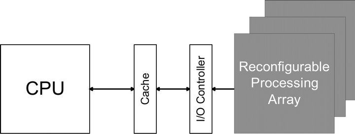
An overview of the current trends and types of architectures has been studied and is shown in Figure 1 [7]. In Figure 1(a), the reconfigurable array is communicating with the general purpose processor through the I/O data bus. In Figures 1(b) and (c), reconfigurable array is moved closer to the processor to decrease the communication cost. In Figure 1(d), the reconfigurable unit is coupled within the processor as a configurable functional unit. With the increasing size and complexity of programmable fabrics and the use of soft core processor, a processor core can also be embedded inside the reconfigurable fabric as shown in Figure 1(e).
These approaches have all been applied in very different application domains. Research has been performed to accelerate cryptographic systems [8], Euclidean distance transformation [9], matrix multiplication [10], and multimedia applications for imaging [11] and video processing [12]. In addition research has been performed into creation of polymorphic processors, which can be reconfigured and applied to multiple application domains [2,3, 13-15].
A common problem for all polymorphic processors is the integration of design flow for both software and reconfigurable hardware. Some work has been performed in auto generation of hardware design targeted at reconfigurable polymorphic processors [16-18]. Most of these approaches use the standard C language to capture program functionality and then through compiler optimization extract sections to be targeted at reconfigurable resources.
3. Reconfigurable Datapath Design
The proposed PolyNoC processor attempts to closely integrate a general-purpose processor with reconfigurable elements. This tight coupling produces a polymorphic reconfigurable processor, which can be reconfigured and extended in real time to include application specific optimizations. Enabling the ability to tailor the processor architecture to the specific application at run time is an important feature of this design.
Prior approaches at integration of reconfigurable elements to general-purpose processor have had various types of implementation ranging from simple attachment as a peripheral to tighter coupling to the memory system or co-processor usage. The PolyNoC processor approaches the design goals by integrating the reconfigurable elements into the foundation of the processor architecture. Unlike previous designs, the datapath of the processor is replaced with a network-on-chip (NoC). Instead of traditional direct wire communication with pipeline registers, the PolyNoC processor utilizes a NoC for all element-
 (a)
(a)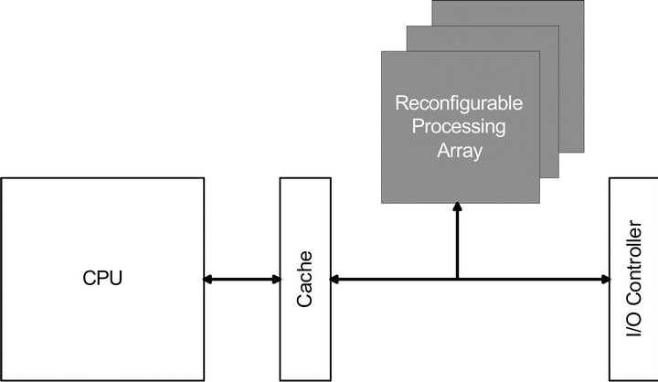 (b)
(b)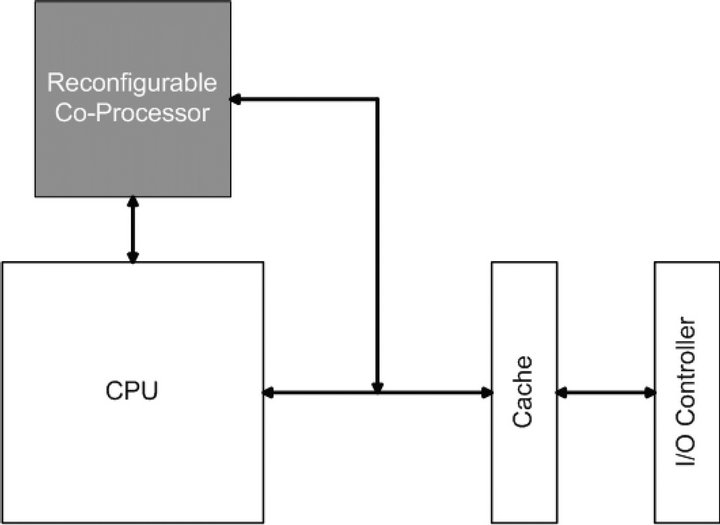 (c)
(c)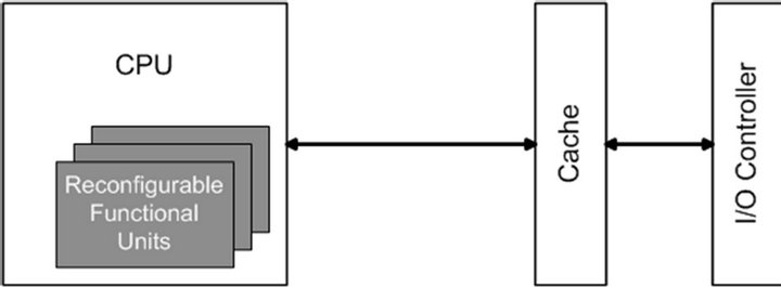 (d)
(d)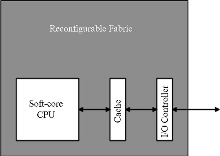 (e)
(e)
Figure 1. Integration of processors and reconfigurable logic.
to-element communication. The use of a NoC provides many advantages to the design and enables the PolyNoC processor to achieve its main goal of real time reconfigurability.
The NoC provides a flexible interconnect and allows new functional computation elements to be added and subtracted in real time. Furthermore, the NoC relieves the designer from strict constraints on placement and ordering of functional elements, as the NoC will provide element-to-element communication regardless of each elements placement. However, the NoC also place many constrains on the overall processor operation. In particular, the latency penalty from the NoC needs to be overcome by the additional advantages provided by the PolyNoC processor, namely the ability to reconfigure the processor to have application specific optimizations.
4. PolyNoC Processor Architecture
The PolyNoC processor architecture can be seen in Figure 2. It consists of a standard instruction and data cache connected to a instruction fetch and decode unit. Next, the instruction is passed to a packetizer. The packetizer wraps the instruction into a NoC packet and then transmits it through the NoC. The packetizer also keeps track of all instruction executions and issues new instructions. The NoC delivers instruction packets to functional units. Each instruction slowly progresses from functional unit to functional unit, stopping to get a subset of execution done.
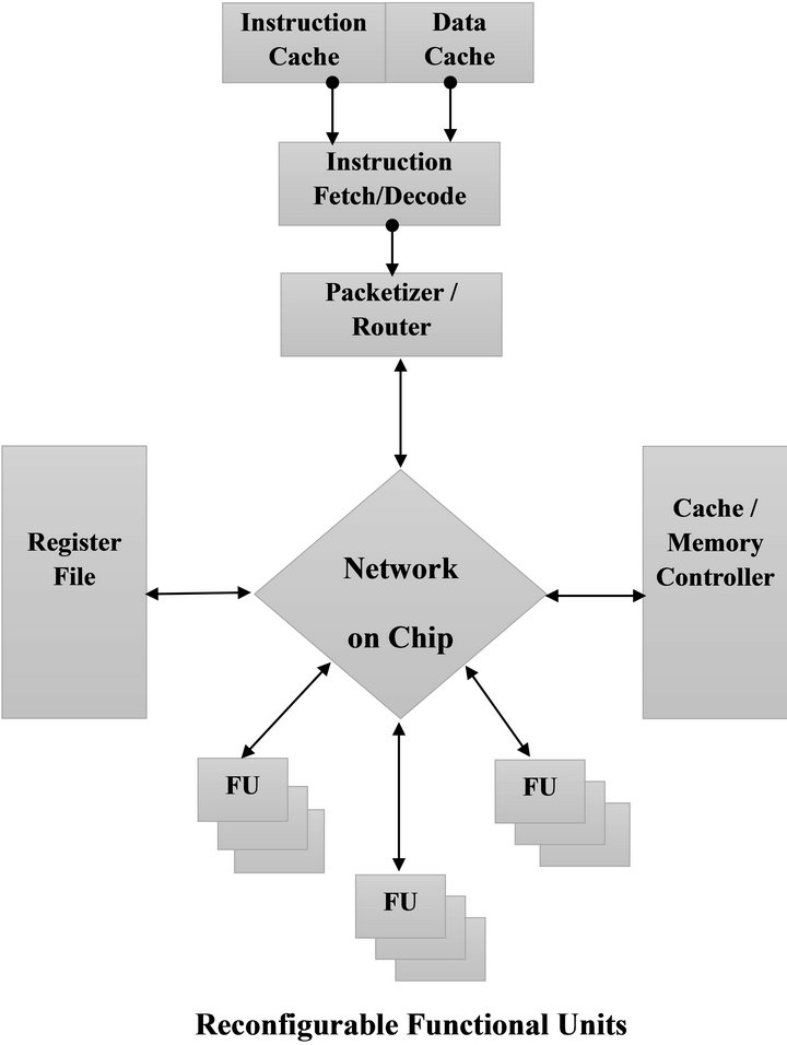
Figure 2. Network-on-chip datapath for polymorphic processors.
Rather than starting from scratch when designing the processor, an existing processor architecture has been adopted and extended. This enables the PolyNoC processor to focus on architectural issues, without dealing with the many contributing factors from compiler and instruction set changes. In addition, the use of a common target processor allows the PolyNoC processor to utilize all existing software and compiler tools available for the target processor. For these reasons, the PolyNoC processor is designed to execute SPARC code and emulate a SPARC processor [19]. Specifically the PolyNoC processor is based upon the LEON3 SPARC processor.
The base level of functional units represents roughly the stages of execution of the SPARC processor the design is modeled on. These base functional units consist of the register file, memory controller, ALU, and FPU. Each functional unit performs computations that are roughly equivalent to the pipeline stages of a LEON3 SPARC processor, the target processor being extended into the PolyNoC. As such, much of the implementation of the basic functional units can remain unchanged from a target general-purpose processor. Only modifications to the input and output communications are necessary.
Besides base functional units, additional functional units can be added to the system. These are represented by blocks of reconfigurable functional units, which can be configured depending on the current application. For example, they can be used to instantiate additional core units such as additional FPU functional elements. By instantiating additional FPU elements, the processor can be tailored to execute a floating-point heavy application. The reconfigurable functional blocks can also be configured to implement custom user logic. By enabling custom logic, the processor can execute new custom instructions. These instructions and logic can be heavily optimized and designed to support a specific application, enabling a great deal of performance increase.
5. Functional Units
5.1. Packetizer
The packetizer, as shown in Figure 3, functions as the primary control of instruction execution. It feeds a program counter (PC) value to the instruction cache unit and accepts the incoming instructions for execution. In order to overcome the increase in execution time caused by the NoC latency and to leverage the flexibility advantages of the NoC datapath, the packetizer allows for multiple instruction issues and out-of-order completion. To accomplish this, the packetizer must track the issuing and completion of all instructions and control the update of the PC.
The packetizer allows for an unlimited number of instructions in flight. This is constrained by the amount of
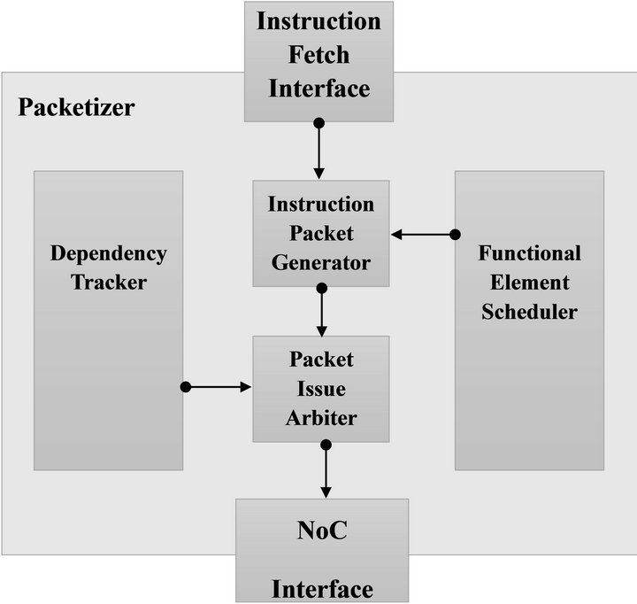
Figure 3. Packetizer block diagram.
instruction level parallelism present in the program. Before issuing any instruction, it is checked for data dependency. This dependency check is performed by the built in dependency tracker detailed in the Section 5.1.1. The dependency tracker analyses 1) data dependency among in-flight instructions and 2) control oriented dependencies from branch instructions. Once the dependency tracker declares the instruction as dependency free, it will be issued for execution and dependency tracker is updated with dependencies of the newly issued instruction.
In order to issue an instruction for execution, it needs to be packetized and transmitted to the NoC. The packetizer decodes the instruction to determine the list of necessary functional elements. For example, a basic ADD instruction will need to visit the register file to obtain input register operands, then the ALU unit for execution of the operation, then return to the register file to write the results into the output register and finally return to the packetizer to update execution completion status. Once an instruction is decoded, the functional element destinations are fed into the functional element scheduler, as detailed in Section 5.1.2. The functional element scheduler will return a network id for each functional element required.
A NoC packet is created to hold the necessary instruction contents. The critical data is the instruction itself and the destination list of functional elements. All of this data are wrapped into a NoC data packet, encoded with the destination of the first functional element and transmitted into the NoC. As instructions are completed they return to the packetizer. The packetizer checks the status of the packet to ensure it was correctly executed. Any instruction that failed execution will return as a trap condition (the packetizer will update the PC to a trap handler). If the instruction was a branch instruction, the new PC value will be included. As a final step, the packetizer will pass the completed instruction to the dependency tracker to remove any dependencies caused by this packet.
5.1.1. Dependency Tracker
The dependency tracker is responsible for determining if a new instruction is dependency free from all currently executing instructions. The tracker accomplishes this task by maintaining an internal list of all data and control dependencies of currently executing instructions. When a new instruction is to be executed, it compares the necessary registers to the dependency lists and determines if it can be executed.
The dependency lists are implemented as simple bit flags. Two 32 bit registers are created to track status of the instruction registers, eight global, eight local, eight input and eight output integer registers and 32 floating point registers. Each bit indicates if a data dependency exists for that register. As each instruction begins execution, it is registered with the dependency tracker. At this time all destination registers being written by the instruction are flagged in the tracking register. When a new instruction is to be executed, all source registers are compared with the tracking registers. If bits corresponding to all source registers are clear, the instruction is free from data dependencies. The final step occurs when an instruction completes execution. In this case the bits corresponding to the destination register are cleared from the tracking list to indicate that there is no longer a data dependency for those registers.
In addition to tracking data dependencies, the dependency tracker also tracks control dependencies. Unlike a traditional datapath, it is difficult to signal flush operations for instructions in flight. As such, no branch prediction is used and all branching cases cause a control dependency. When a control instruction is in-flight all future instructions hold off on execution until resolution of the branch instruction. The dependency tracker provides this tracking for the packetizer to control instruction issuing. In addition, as the register windows are affected by a SAVE or RESTORE instruction, they too exhibit a control dependency. All instruction must await completion before execution.
The dependency tracker is critical to the overall operation of the PolyNoC processor. Together with the packetizer it enables a multiple issue instruction datapath. Since, the NoC datapath imparts latency penalties to execution compared to a traditional processor, a large mitigating factor provided by the PolyNoC processor is the ability to extract instruction level parallelism from the instruction stream. The dependency tracker is crucial for this ability. It checks each subsequent instruction for dependencies. If the instruction is found to be free of dependencies then it is executed at the same time as the prior instruction. This behavior helps to keep the execution elements fully utilized and provides significant benefits to overall execution time.
5.1.2. Functional Element Scheduler
The functional element scheduler provides addressing and scheduling of functional elements to the packetizer. It maintains a list of all functional elements, their NoC addresses, and the functional element type. For simple cases with only one instance of each functional element, it simply returns the address of the element when a request is made for an element of that type. For cases when more than one element of a type has been created, it performs scheduling. The current PolyNoC processor performs scheduling through a round robin scheduling algorithm. This schedules all functional elements equally and distributes instruction load evenly. It also benefits from a very simple implementation and critically requires no signaling from any functional element. For these reasons, it was chosen as the scheduling algorithm for the PolyNoC processor. Further performance gains can be made through more advanced and intelligent scheduling algorithms since the round robin algorithm does not take into account current status of functional elements.
5.2. Register File
The register file implements and provides access to all processor registers. It implements the register definitions according to the SPARC architecture [19]. It defines a set of overlapping windows general-purpose instruction registers. These overlapping windows provide functionality to pass parameters between subroutine calls. The execution of SAVE and RESTORE instructions allow the adjustment to a new register window, which contains shared output and input registers for different window values.
The register file further implements 32 floating-point general-purpose registers. These registers are usable by all floating-point instructions. In addition to generalpurpose registers, the register file also implements the SPARC control and status registers. These control and status registers provide access to configuration and status of a SPARC processor and are necessary for compliance with SPARC execution model. Some status registers are critical in execution, for example the processor state register (PSR) holds the contents of the condition codes. The register file also supports the execution of the SAVE and RESTORE instructions, shifting the register window up or down. All of these options combine to make a fully compliant SPARC register set.
5.3. Memory Controller
The memory controller enables access to external addressed memory. This supports both reading and writing of external memory. The basic functionality of the memory controller is simple and its implementation is straightforward. The SPARC standard defines the primary external memory bus to use the AMBA AHB bus protocol. Therefore, the PolyNoC processor and the memory controller implements an AMBA AHB master controller for accessing the bus.
In addition to providing access to the external memory space, small amount of configuration memory space must also be implemented within the memory controller. This memory space provides plug-n-play capabilities for the AHB bus, enabling AHB bus slaves to be added and configuration options and memory address locations stored. This configuration space is crucial to the memory controller master controller and used to generate chip selects and initiate access to AHB slaves.
5.4. Arithmetic Logic Unit
The ALU performs all integer arithmetic and logic computations for instructions. In addition to execution of basic instructions, the ALU also computes memory addresses and branch and jump targets. The ALU must be robust enough to support arithmetic and logic operations for all data types as required by the SPARC instruction set. ALU performance can have a significant impact on over all processor performance but from the standpoint of the operation of the PolyNoC processor, it does not present any new challenges.
5.5. Floating-Point Unit
Like the ALU, the FPU performs all arithmetic and logic computations for floating point operations. This implements all basic computations on standard IEEE-754 floating-point numbers. The implementation can vary widely and have performance impacts on the PolyNoC processor. A potential advantage of the PolyNoC processor is the ability to incorporate multiple or even different FPU implementations allowing for design choices that are not feasible with a traditional general purpose processor.
6. NoC Interconnect
The network-on-chip (NoC) interconnect links all functional elements together and enables communication among them. Any instruction will traverse the NoC multiple times during execution. For the basic SPARC instruction with just the core functional elements, it will require 3 to 5 trips through the NoC to complete execution of each instruction (similar to pipeline stages). Therefore, performance of the NoC links is very important to the overall performance of the PolyNoC processor.
The NoC should also be able to provide a scalable architecture with a dynamic layout. The PolyNoC processor’s main advantages are in flexibility and reconfiguration. The greatest performance gains are obtained by real time reconfiguration of the number and type of functional elements. The NoC must be able to support to addition and subtraction of functional elements with no impact to overall NoC performance. In addition, due to the heavy dependency on latency, the NoC needs to scale well. As additional functional elements are added and the total number of nodes within the NoC increases, the average latency for travel over the NoC should not grow rapidly. If the NoC latency increases too quickly, any performance gain from additional functional elements can be lost due to the penalties from increased execution time.
The NoC also needs to be able to support a flexible packet type and size. Each NoC packet will need to encapsulate an instruction and all necessary information for execution of that instruction. Data carried by the packets will vary between each instruction. To save on overall packet size, the packet should allow for a flexible packet size to shrink or grow according to the demands of the individual instruction. Packet structure should have a minimum amount of overhead when encapsulating an instruction and data. Minimizing this overhead reduces the overall packet size and lower the overall bandwidth requirements for interconnect links.
The traffic generation for the PolyNoC processor is dependent on instruction execution. As a result, the traffic load is reduced compared to other NoC systems. The execution of instructions tends to be limited by the computational time of the functional elements. This stark limit on the number of instructions currently executing makes for a low overall bandwidth requirement. The low bandwidth requirement provides one of the main NoC design techniques to improve performance. The PolyNoC processor can run the NoC communications on a separate and higher frequency clock then the functional elements. Since latency is a critical NoC parameter, the higher NoC clock allows compensating for the NoC delay. The latency figure is computed based on the NoC clock. When running the NoC at a higher clock frequency, the overall NoC delay is drastically reduced. In many cases, it seems reasonable to run the NoC clock at 4 or 8 times the functional element clock. This provides the ability to have up to 4 or 8 clock cycles of latency for NoC transmission within a single functional element execution clock cycle, potentially hiding all latency penalties during execution.
The PolyNoC processor presents a very unique set of requirements for a NoC. In addition, the traffic generation is the result of instruction execution. This type of traffic load is uncommon and has not been studied in depth. For these reasons, it is difficult to approach the design of the NoC from theoretical statistical approach, as is often applied during NoC research. Instead, this work has focused on an experimental approach. A simulator for NoC design exploration has been created and various NoC design parameters have been modified and tested to determine the impact on NoC performance.
7. NoC Architecture Exploration
This section presents an exploration of the architectural and topology issues impacting the performance of the PolyNoC processor [3]. The Network Simulator 2 (ns-2) [20] is utilized as a network simulation platform. Ns-2 is extended to simulate the execution of the PolyNoC processor. With this simulation platform, instruction trace data from real world benchmark programs can be run through the simulator and it provides an excellent research tool for the study of the PolyNoC processor.
The ns-2 simulator is a discrete event simulator targeting networking research. It has been used in a wide variety of networking research including simulation of NoC architecture and protocols. It provides support for a wide range of networking techniques, in addition to robust access to the underlying framework to allow for custom modification and extension of the simulator. Ns-2 is implemented in C++ with an interface layer based upon OTcl. All major simulation objects are created as discrete objects in C++. It provides very fine grained access to all objects within a network, packet structure, link parameters, routing agents, network node modeling, and support for modeling of all layers of the OSI stack. Beyond the extensive list of built in networking objects, ns-2 provides the ability to extend the platform to incorporate new designs and techniques. This extensibility is heavily utilized for modeling the PolyNoC network execution.
Ns-2 was modified and extended to support simulation of a processor executing with a NoC datapath. To facilitate this, a new custom set of applications, agents, nodes, and packets were added to the ns-2 simulator. All functional units within the processor are represented in the ns-2 simulator as an application. These applications then communicate with each other using the ns-2 node network simulation.
Using the ns-2 simulator, four main network topologies were studied and compared as shown in Figure 4. These topologies consist of Ring, Modified Ring, 2D Mesh, and Crossbar architectures. The ring architecture provides a simple baseline implementation. Due to the fact that a processor datapath is highly sequential, it is very similar to the flow of data through a traditional datapath. The modified ring structure attempts to provide a more robust scalability than the standard ring. In this architecture similar functional units are placed in parallel on the ring structure. This incurs a minor increase in link cost, but provides the same total delay over the ring regardless of number of functional units instantiated. The
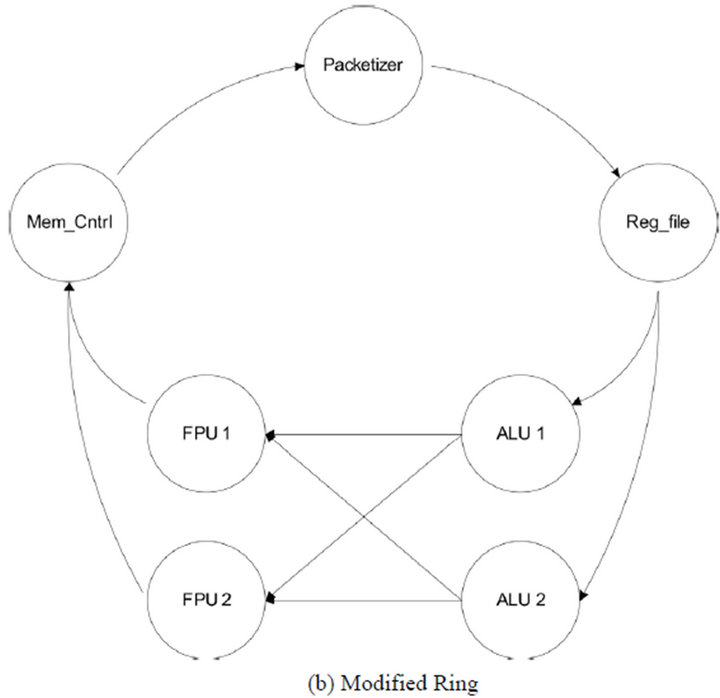
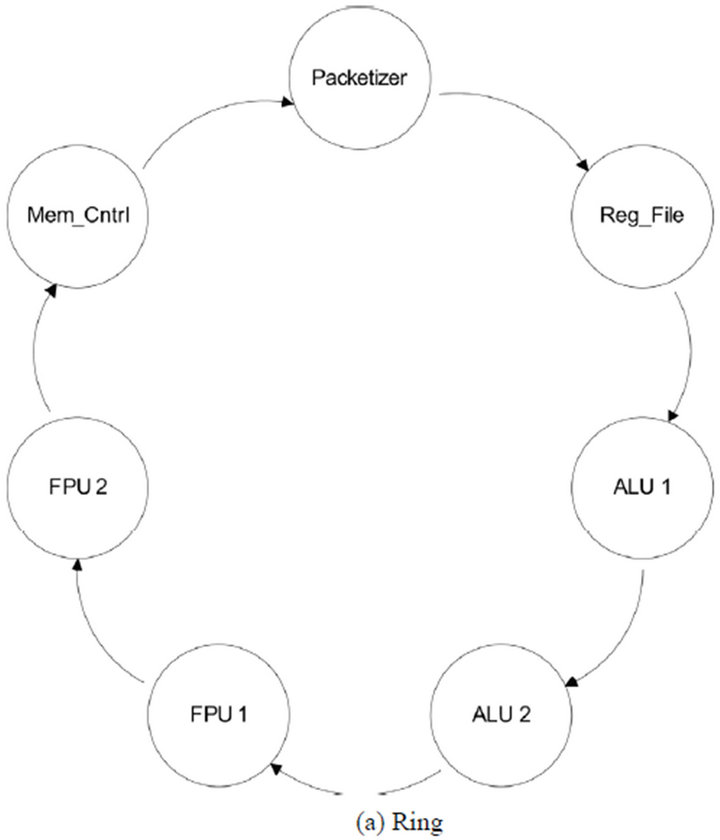
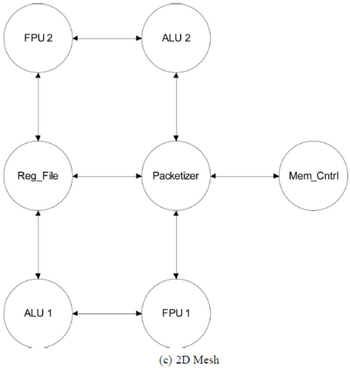

Figure 4. NoC topologies investigated.
next architecture studied is the standard 2D mesh architecture. The architecture is a rectangular layout with bidirectional links between neighboring nodes. The final architecture explored is a crossbar. The crossbar architecture is an extreme architecture in which every node has a link to every other node. This shrinks all communications to only a single hop away, but comes with a very sharp increase in link cost as the network scales in nodes. Figure 5 shows an example ns-2 script for evaluating the performance of a simple PolyNoC processor architecture (i.e., ring topology with only basic functional elements).
In addition to exploration of the various topologies, the impact of increasing the number of functional units was also explored. The increase in the number of functional units and the ease of integration to the processor design is fundamental to a polymorphic processor. Increasing the number of computational functional units (both ALU
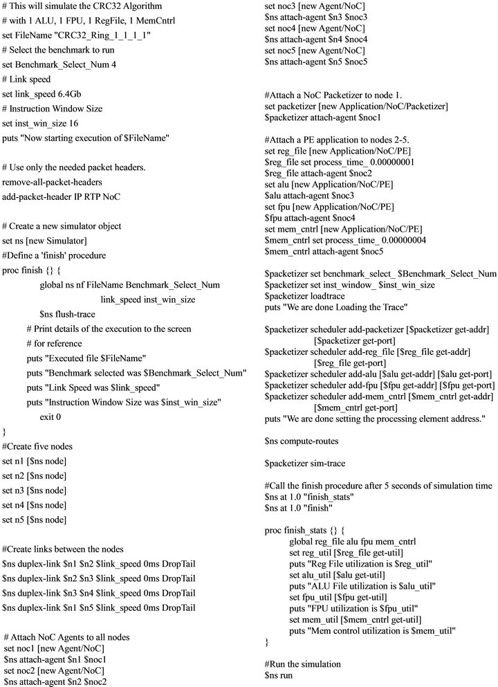
Figure 5. Sample ns-2 script for instantiating a PolyNoC processor architecture (ring topology).
and FPU) directly impacts the overall performance.
8. Simulation Results
For performance analysis, benchmark programs have been compiled for execution on the PolyNoC processor simulator. The benchmarks come from the well-known MiBench benchmark suite [21]. MiBench provides a set of commercially representative embedded systems programs. Extracted from this set and used are the CRC32, FFT, IFFT, ADPCM.encode, ADPCM.decode, and BasicMath benchmark. This set of benchmarks provides a varied application load to get an initial impression on the performance of the proposed processor design.
• CRC32-Performs a 32-bit Cyclical Redundancy Check on input data. CRC checks are often used as error checking during data transmission.
• FFT/IFFT-Performs a fast Fourier transform or an inverse fast Fourier transform on an input data array. The FFT is used for frequency analysis during signal processing in a very wide range of application domains.
• ADPCM encode/decode-Adaptive Differential Pulse Code Modulation is a variation of the more common Pulse Code Modulation (PCM). This variation takes in 16-bit linear PCM samples and converts them to 4-bit samples providing significant compression. This algorithm is executed over samples of speech.
• BasicMath-Performs common mathematical computations that very frequently do not have hardware implementations. In this benchmark cubic function solving, integer square roots and angular conversion are computed.
Benchmark programs are first run on the TSIM LEON3 SPARC simulator. As the benchmarks are executed, a trace of all executed instructions is captured. This provides a cycle accurate, in-order instruction trace of the benchmark when it is executed on a commercially available SPARC processor. The instruction trace is then used as input to the ns-2 based simulator. The use of this trace provides an accurate traffic model of the execution of the PolyNoC processor. Trace based traffic model accurately represents the transmission of instruction packets into the NoC by the packetizer unit. This allows for very basic modeling of the instruction execution time, without being concerned with the full simulation of SPARC processor, significantly easing the implementation and execution time of the simulator.
The total execution time for all benchmarks can be seen in Tables 1-4. Table results show the total number of cycles to execute each benchmark with four different topologies. The total cycle count is an accurate measure of the performance of the processor. A higher performing processor will be able to execute more instructions in less

Table 1. Ring execution time (clock cycles).
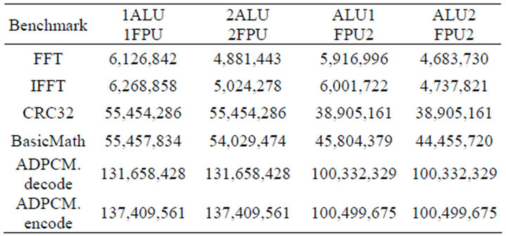
Table 2. Modified ring execution time (clock cycles).

Table 3. 2D Mesh execution time (clock cycles).
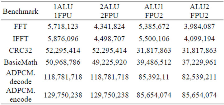
Table 4. Crossbar execution time (clock cycles).
time. All the values presented were obtained using an instruction window size of 16, with an assumed NoC clock rate 8 times the datapath clock. It is reasonable assume the NoC clock can run at a higher rate then the functional elements datapath clock. This prevents the PolyNoC processor from becoming NoC bound wherein instruction execution time is limited by the NoC latency and the increase from additional functional units provides no performance gains.
Results show that all architectures exhibit scalability, and increased performance as the number of functional units increase. It can be seen that they all perform similar when only a single functional unit of each type is used. The advantages only become significant as the number of functional units increase. As the number of functional units is increased modestly from one to two ALUs/FPUs, significant performance improvements are achieved. It is important to note that a PolyNoC processor would allow this performance boost to be selectively applied during run time as reconfigurable elements are configured to act as additional functional units. The applications that are heavily FPU operation oriented benefit most from additional FPU elements, similarly ALU oriented benchmarks get more performance from an increase in number of ALU elements.
The ring architecture is simple and has very low resource cost however, its performance is lacking. The performance increase from additional function units is cannibalized by increased packet delay through the network. When more functional units are added, the latency of the overall NoC transmission increases due to the need to traverse the additional intermediate nodes. The additional penalty from NoC latency counteracts any performance gains from more functional elements, and in some cases actually lowers the overall performance of the PolyNoC processor. The modified ring architecture helps to mitigate the additional penalty from extra functional elements by eliminating the growth of delay when adding more functional units. In this case, the additional units do not increase the latency from NoC transmission. However, it still exhibits a similar weakness in overall structure; the ring based architecture delay is too high and prevents optimal processor execution either for the original ring or modified ring. On the other hand, the 2D Mesh architecture looks very promising as a candidate for NoC architecture. The max number of nodes compared to delay grows at a polynomial rate, producing a slow increase in delay relative to increase in total number of functional elements. Furthermore, for small mesh sizes, a large portion of communication occurs exclusively between neighboring nodes, allowing for an optimal 1 cycle delay time. This enables minimal latency. Near neighbor effect can also be maximized by careful layout of the 2D mesh. The mesh structure should be laid out such that node that frequently communicate with each other. For example, majority of instructions transits to the ALU after visiting the register file. Finally, the Crossbar architecture represents a reference point for comparison. It provides a connection from every node to every other node and it allows for a constant delay time of 1 clock for all packet transmissions. This can be seen as an upper limit to performance gains independent of architectural choices. This reference point is a valid comparison for the other topologies. With all packet delays at an optimal 1 cycle delay, it achieves the highest PolyNoC performance. The overall performance is now limited by the performance of the functional elements, and the overall parallelism that can be extracted from the instruction stream.
Both the performance and the hardware resource consumption of the architectures can be seen in Figure 6. This figure presents the cost of each architecture based on the total number of individual point to point unidirectional links. Results indicate the superior performance of the 2D Mesh architecture. With much lower total cost, it is able to achieve a performance that is only slightly reduced from the upper limit set by the Crossbar implementation.
In conclusion, the 2D mesh structure is able to outperform all other topologies studied. It is able to scale well with additional functional units. As the more units are added, the additional latency in NoC transmission is controlled and overall system performance goes up. In general, the performance of the 2D mesh is fairly close to the theoretical maximum demonstrated through the crossbar architecture. 2D mesh structure also performs best at cost scaling. The link cost for point to point links grows very slowly compared to other implementation, while still providing large gains in total PolyNoC performance.
The final PolyNoC processor design with incorporation of optimal parameters can be seen in Figure 7. It shows the detailed layout of the NoC architecture and the placement of reconfigurable arrays and basic functional units. From the topology results, it is clear that the 2D mesh architecture provides the optimal balance of performance and cost. For these reasons it is chosen as the basis of the NoC architecture. This design provides a basic 4 × 4 mesh layout. This is a relatively small layout which could easily be scaled to larger size. 4 × 4 layout provides space for all basic units and a total of 11 reconfigurable arrays for application specific functional units. The design makes use of 2-input, 3-input, and 4-input switches as the backbone of the communication infrastructure. Each switch is interfaced to a single functional unit. Functional units can be a basic unit supporting the execution of the standard SPARC ISA, or a reconfigurable unit supporting the creation of new application specific instruction.
9. Conclusion
In this work, a new reconfigurable processor architecture has been introduced. Traditional fixed pipeline based datapath is replaced with a reconfigurable NoC based communications channel. Functional elements can communicate with others elements and they can be added and reconfigured dynamically enabling polymorphic operations. Several NoC topologies were explored to find the

Figure 6. Cost vs performance analysis of different NoC topologies and number of functional units.
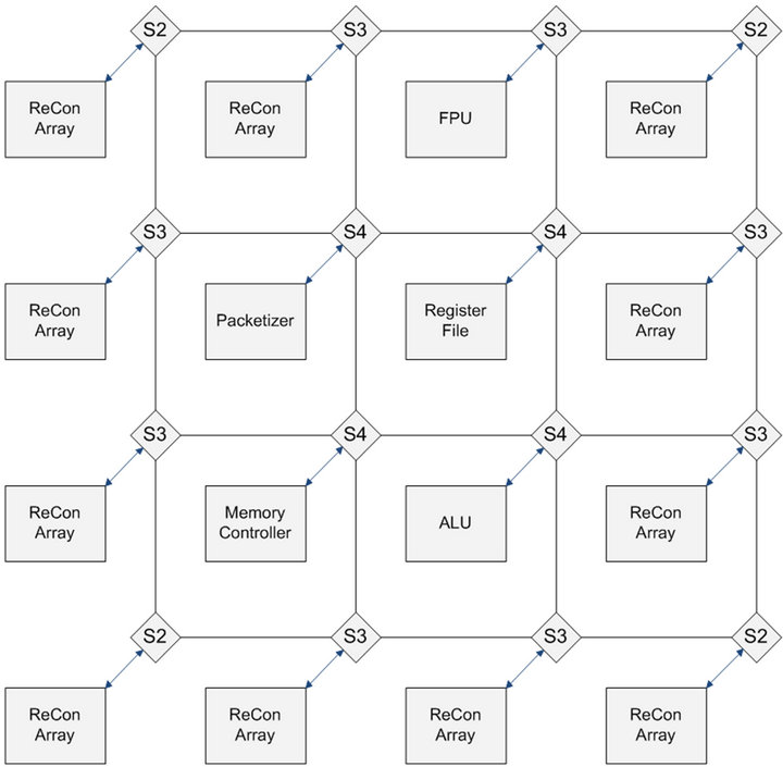
Figure 7. 4 × 4 2D mesh architecture.
optimal organization for a NoC based datapath. Industry standard MiBench benchmarks were used to study the execution of the PolyNoC processor. Results demonstrate that the PolyNoC processor provides significant advantages in flexibility of design. It is able to support both very large stream based optimizations (i.e., computation of ADPCM block based encoding), while also performing very fine grained, highly coupled custom instruction group optimizations, (i.e., optimization of the CRC32 hash update loop). Therefore, PolyNoC processor allows easy incorporation of reconfigurable arrays, both coarse and fine grained, for application specific optimizations.
REFERENCES
- “International Technology Roadmap for Semiconductors,” 2009. http://www.itrs.net/Links/2009ITRS/Home2009.htm
- D. Hentrich, E. Oruklu and J. Saniie, “Polymorphic Computing: Definition, Trends, and a New Agent-Based Architecture,” Circuits and Systems, Vol. 2, No. 4, 2011, pp. 358-364. doi:10.4236/cs.2011.24049
- J. Weber, E. Oruklu and J. Saniie, “Architectural Topologies for NoC Datapath Polymorphic Processors,” IEEE International Conference on Electro/Information Technology, Mankato, 15-17 May 2011, pp. 1-6.
- K. Compton and S. Hauck, “Reconfigurable Computing: A Survey of Systems and Software,” ACM Computing Surveys, Vol. 34, No. 2, 2002, pp. 171-210. doi:10.1145/508352.508353
- Z. Guo, W. Najjar, F. Vahid and K. Vissers, “A Quantitative Analysis of the Speedup Factors of FPGAs over Processors,” FPGA Proceedings of the ACM/SIGDA 12th International Symposium on Field Programmable Gate Arrays, New York, 2004, pp. 162-170.
- K. Underwood, “FPGAs vs CPUs: Trends in Peak Floating-Point Performance,” FPGA Proceedings of the ACM/ SIGDA 12th International Symposium on Field Programmable Gate Arrays, New York, 2004, pp. 171-180.
- T. Todman, G. Constantinides, S. Wilton, O. Mencer, W. Luk and P. Cheung, “Reconfigurable Computing: Architectures and Design Methods,” IEEE Proceedings of Computers and Digital Techniques, Vol. 152, No. 2, 2005, pp. 193-207.
- R. Cheung, N. Telle, W. Luk and P. Cheung, “Customizable Elliptic Curve Cryptosystems,” IEEE Transactions on Very Large Scale Integration Systems, Vol. 13, No. 9, 2005, pp. 1048-1059.
- P. Baglietto, M. Maresca and M. Migliardi, “Euclidean Distance Transform on Polymorphic Processor Array,” CAMP Proceedings of Computer Architectures for Machine Perception, Como, 18-20 September 1995, pp. 288- 293.
- G. Kuzmanov and W. van Oijen, “Floating-Point Matrix Multiplication in a Polymorphic Processor,” ICFPT International Conference on Field-Programmable Technology, Kitakyushu, 12-15 December 2007, pp. 249-252.
- S. Chai, S. Chiricescu, R. Essick, B. Lucas, P. May, K. Moat, J. Norris, M. Schuette and A. Lopez-Lagunas, “Streaming Processors for Next Generation Mobile Imaging Applications,” Communications Magazine, Vol. 43, No. 12, 2005, pp. 81-89. doi:10.1109/MCOM.2005.1561924
- H. Hubert and B. Stabernack, “Profiling-Based Hardware/ Software Coexploration for the Design of Video Coding Architectures,” IEEE Transactions on Circuits and Systems for Video Technology, Vol. 19, No. 11, 2009, pp. 1680-1691. doi:10.1109/TCSVT.2009.2031522
- C. Rupp, M. Landguth, T. Garverick, E. Gomersall, H. Holt, J. Arnold and M. Gokhale, “The Napa Adaptive Processing Architecture,” IEEE Symposium on Proceedings of FPGAs for Custom Computing Machines, 17 April 1998, pp. 28-37.
- S. Vassiliadis, S. Wong, G. Gaydadjiev, K. Bertels, G. Kuzmanov and E. Panainte, “The Molen Polymorphic Processor,” IEEE Transactions on Computers, Vol. 53, No. 11, 2004, pp. 1363-1375. doi:10.1109/TC.2004.104
- N. Vassiliadis, G. Theodoridis and S. Nikolaidis, “The Arise Approach for Extending Embedded Processors with Arbitrary Hardware Accelerators,” IEEE Transactions on Very Large Scale Integration Systems, Vol. 17, No. 2, 2009, pp. 221-233.
- M. Gokhale and J. Stone, “NAPA C: Compiling for a Hybrid Risc/Fpga Architecture,” IEEE Symposium on Proceedings of FPGAs for Custom Computing Machines, 17 April 1998, pp. 126-135.
- J. Cong, G. Han and Z. Zhang, “Architecture and Compiler Optimizations for Data Bandwidth Improvement in Configurable Processors,” IEEE Transactions on Very Large Scale Integration Systems, Vol. 14, No. 9, 2006, pp. 986-997.
- S. Gupta, N. Dutt, R. Gupta and A. Nicolau, “SPARK: A High-Level Synthesis Framework for Applying Parallelizing Compiler transformations,” Proceedings of the 16th International Conference on VLSI Design, New Delhi, 4-8 January 2003, pp. 461-466.
- The SPARC Architecture Manual, Version 8, Sun Microsystems, 1992. http://www.sparc.org/standards/V8.pdf
- Ns-2, The Network Simulator. http://nsnam.isi.edu/nsnam/index.php/Main_Page
- M. Guthaus, J. Ringenberg, D. Ernst, T. Austin, T. Mudge and R. Brown, “Mibench: A Free, Commercially Representative Embedded Benchmark Suite,” IEEE International Workshop on Workload Characterization, December 2001, pp. 3-14.