Circuits and Systems
Vol. 3 No. 1 (2012) , Article ID: 16608 , 13 pages DOI:10.4236/cs.2012.31008
Thermodynamical Phase Noise in Oscillators Based on L-C Resonators (Foundations)*
Group of Microsystems and Electronic Materials (GMME-CEMDATIC), Universidad Politécnica de Madrid (UPM), Madrid, Spain
Email: joseignacio.izpura@upm.es
Received September 19, 2011; revised October 19, 2011; accepted October 27, 2011
Keywords: Admittance-Based; Noise Model; Energy Dissipation; Energy Conversion into Heat; Phase Noise
ABSTRACT
By a Quantum-compliant model for electrical noise based on Fluctuations and Dissipations of electrical energy in a Complex Admittance, we will explain the phase noise of oscillators that use feedback around L-C resonators. Under this new model that departs markedly from current one based on energy dissipation in Thermal Equilibrium (TE), this dissipation comes from a random series of discrete Dissipations of previous Fluctuations of electrical energy, each linked with a charge noise of one electron in the Capacitance of the resonator. When the resonator out of TE has a voltage between terminals, a discrete Conversion of electrical energy into heat accompanies each Fluctuation to account for Joule effect. This paper shows these Foundations on electrical noise linked with basic skills of electronic Feedback to be used in a subsequent paper where the aforesaid phase noise is explained by the new Admittance-based model for electrical noise.
1. Introduction
As it is well known, no voltage V0 set on a capacitor of capacitance C can remain constant with time t. The first reason is a self-discharge of C through its resistance R, because capacitors offering a pure capacitance at  do not exist [1]. This leads to an exponential decay with time constant
  of any
  set in C that ends with a null V0 only on average:
 , because the thermal fluctuation
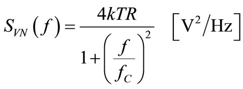
  J per degree of freedom sets an ac voltage noise in C whose spectral density is shaped by R to give a mean square noise voltage
  V2 on C. This last sentence summarizes the new model for electrical noise used recently to explain the flicker noise found in vacuum devices [1] and the 1/f excess noise of Solid State ones [2]. This new model considers that the noise of resistors and capacitors is born in their capacitance C between terminals and that their conductance
  shunting C only shapes the noise spectrum to accomplish Equipartition as it can be deduced from [3]. The complex Admittance this new model uses allows to handle Fluctuations and Dissipations of electrical energy in time [4], thus excelling today’s model based on Real Conductance that neither considers Fluctuations of this energy, nor distinguishes Dissipation of electrical energy from its Conversion into heat as we will do.
Shunting the R-C parallel circuit of a capacitor by a finite inductance L ≠ 0, an L-C-R parallel resonator of resonance frequency f0 appears. The role of this L can be seen as a feedback current that being proportional to the voltage v(t) on C, has –90˚ phase lag under sinusoidal regime (SR). This feedback in quadrature with v(t) that affects f0, leads to the feedback-induced phase noise that we showed for oscillators based on resonant microcantilevers in [5]. This Technical phase noise due to a deficient phase control of the feedback adds to the non technical, but Thermodynamical phase noise we will explain for oscillators with perfect loops where current feedback to the resonator is exactly in-phase with its voltage v(t) for Positive Feedback (PF) or exactly at ±180˚ for Negative Feedback (NF). This prevents the addition of Technical phase noise to the Thermodynamical one sketched in [6] that we will explain, which is linked with resonator’s losses represented by its R and with noise added by the feedback electronics, both considered by the noise figure F of Leeson’s pioneering work [7]. We will show the theory behind Leeson’s empirical formula and behind the Line Broadening that these oscillators show around their mean oscillation frequency f0 [8]. The general theory on phase noise of [9,10] and the references therein are valuable introductions on this topic that we will define as: the impossibility to achieve a periodic Fluctuation of charge in L-C resonators.
Although phase noise means that the energy of the oscillator’s output signal is spread around f0 (e.g. its spectrum is not a d(f – f0) function or “line”), the amount of this spreading due to each feedback of the oscillator is not obvious. Hence the reason to start with a “special oscillator” giving a signal of frequency  whose phase noise can’t be defined because this signal doesn’t change phase in a finite time interval, but where Dissipations of electrical energy enhanced by a Clamping Feedback can be shown easily, as well as the Pedestal of electrical noise that results when this feedback is confused by noise not in phase with the output signal it tracks. This paves the way towards actual oscillators of f0 ≠ 0 that we will study in a subsequent paper under the same title, where Fluctuations and Dissipations of energy will produce, respectively, the Line Broadening of the output spectrum and the Pedestal far from f0, both sketched in [6]. Our results will show that L-C oscillators show phase noise because they are Charge Controlled Oscillators for an unavoidable charge noise power of 4FkT C2/s [4] that disturbs their otherwise periodic fluctuation of charge expected from the exchange of energy between their opposed susceptances due to L and C.
This paper is organized as follows. In Section 2 we consider Fluctuation, Dissipation and Feedback around a capacitor to show their basic interaction. Section 3 shows the difference between Dissipation of electrical power in Thermal Equilibrium (TE) and its Conversion into heat in capacitors and resistors out of TE that allows to understand why electrical noise doesn’t depend noticeably on the power being converted into heat out of TE when the temperature rising is low, although this Converted power can be millions of times larger that the electrical power Dissipated in TE following to [4]. Some relevant conclusions used to explain phase noise in a subsequent paper under the same title, are summarized the end.
2. Fluctuation, Dissipation and Feedback around a Capacitor
The circuit of Figure 1(a) shows the equivalent circuit of a capacitor of capacitance C or resistor of resistance R at low f. This circuit allowing Fluctuations of electrical energy as fast displacements currents in C, each triggering a subsequent Dissipation of energy by a conduction current through R, is a physically cogent circuit for electrical noise [4]. At its cut-off frequency  the current iQ(t) through C and the current iP(t) through R have equal magnitude under SR. This fc separates the low-f region
 , where the active power dissipated in R surpasses the reactive power fluctuating in C, from the high-f region
  where the situation is the opposed one. This device is a good resistor when its ratio
 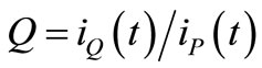 is low (e.g. at
 ) because it mostly dissipates electrical energy. At high f, however, it is a good capacitor where electrical energy mostly fluctuates because the ratio Q is high. Thus, the quality factor Q(f) sets the dissipative or reactive character of this device. Figure 1(b) shows the time evolution of a voltage V0 existing at
  on C. This voltage endures an energy
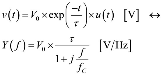
  J stored in C out of TE that can be converted into heat “in R”. This gives the exponential decay of v(t) with time constant
  whereas the stored energy decays with a time constant
 .
.
Let’s consider an spectrum analyzer sampling v(t) from  to
to  (e.g.
(e.g. ) to obtain its Fast Fourier Transform (FFT). Because the energy content of v(t) after tend is small, this FFT analyzer having recorded nearly all the energy U0 of this Signal would give a Lorentzian spectrum SVS(f) like that of Figure 1(c).
This v(t) signal, viewed as a single decay born in  and its Fourier transform are:
 (1)
(1)
 (a)
(a)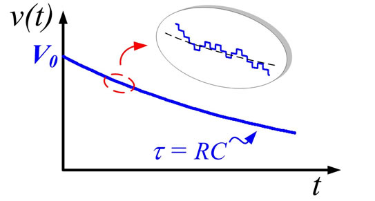 (b)
(b) (c)
(c)
Figure 1. (a) Noise circuit of resistors and capacitors; (b) Time evolution v(t) of a voltage V0 stored in C at t = 0; (c) Unilateral spectrum of v(t) (see text).
thus giving this unilateral Lorentzian spectrum for v(t):
 (2)
(2)
Integrating (2) from  to
to  by its equivalent Bandwidth
 , we obtain:
 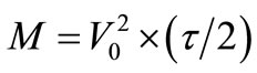 V2 ´ s, a value that also appears by integrating the square of the decay (1) from t = 0 to
  (Parseval’s Theorem). Thus, M is not the electrical energy UDS converted into heat by v(t) driving R from t = 0 to
 . This energy is:
  J, thus suggesting that
  will contain some rate factor l (s–1) to cancel the time unit of (2) as well as a capacitive factor to convert V2 into J. This paves the way to see Conductance
  as a rate of discrete chances to exchange electrical energy [4] that makes easier the understanding of phase noise. Added to the Signal spectrum (2) there will be a small Noise spectrum due to the thermal charge noise of C viewed as the
  noise of this capacitor or as the Johnson noise “of its R”. This noise comes from a random series of Thermal Actions (TA) on C, each being an impulsive charge variation of one electron between its plates, which are the terminals of R [4]. Each TA sets a voltage step of
  V in C that decays with time constant τ as C discharges through R. These decays called Device Reactions (DR) in [4] are sketched in Figure 1(b). Each DR endures a slower charge noise of one electron with opposed sign to that of its preceding TA. This random series of DRs with zero mean (e.g. the number of positive and negative DR’s is equal on average) keeps the native spectrum of its basic impulse (Carson’s Theorem). The charge noise due to these (TA-DR) pairs has an average power
 that gives a noise vn(t) whose mean density is [4]:
 (3)
(3)
where k is Boltzmann constant and T temperature. It’s worth noting that replacing C by αC in Figure 1(a) the amplitude of these DRs will change from  V to
V to  V and their time constant from τ to ατ, thus keeping the amplitude of (2) and (3), but shifting their cut-off frequency to
 . This way, electrical noise obeying Equipartition keeps
  J as the Thermal fluctuation in C [4]. This change in C will appear later as an effect due to a feedback acting on the circuit of Figure 1(a).
Since the FFT analyzer considers that the Signal (2) repeats each  seconds (otherwise the mean Signal power would be null), we have to multiply (2) by the rate
  to have some Signal power sustained in time to compare with the mean Noise power that thermal activity sustains in time. This way the unit of time (s) disappears in (2), which acquires the familiar units V2/Hz of “power density on 1 Ω”. This allows comparing the two Lorentzian spectra “seen” by the FFT analyzer: the big one of the “repetitive” Signal given by (2) in V2/Hz units and the small Noise spectrum of (3). Let’s have some figures at room T with
  V for
V for  pF and
  GΩ (
GΩ ( s). From (2) and (3) the Signal/Noise ratio of the above spectra is higher than 107, thus meaning that the Lorentzian noise spectrum would be buried by the Signal one of equal shape, or buried in its “roughness” coming from mathematical rounding in the FFT algorithm, quantization noise, etc.
For its utility to start oscillators, let’s use electronic feedback to generate a voltage V0 in the capacitor of Figure 1 from its own thermal noise and to sustain it in time as close as possible to a dc reference VRef. Figure 2 shows a PF adding a resistance –R in parallel with C by feeding-back a current , proportional to the voltage sampled by the feedback network of transconductance
 . This PF aims at compensate losses of electrical energy taking place by R when C stores an energy that differs from its value in Thermal Equilibrium (TE). Thus, this PF doesn’t remove losses in R: it only compensates them. This βY leading to a loop where power lost in R and power delivered by the PF are equal (Gain = Losses condition) does not mean that this PF removes the losses of this “resonator of
 ”. Contrarily, this PF sustains in time resonator’s losses by injecting the same power it loses through R, thus sustaining in t a Conversion of electrical energy into heat in this resonator that having a non null voltage V0, is thus out of TE. This distinction between Dissipation of electrical energy [4] and Conversion of electrical energy into heat that occurs out of TE will be clarified later.
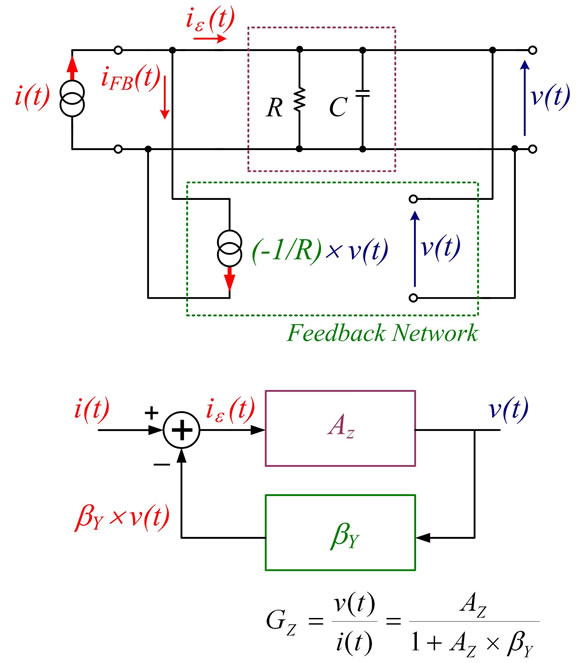
Figure 2. Feedback scheme allowing to compensate losses of energy in R without changing the value of C.
With  V and
V and  MΩ, the circuit of Figure 2 would convert electrical energy into heat at a rate of 10 µJ per second (10 µW) that its PF would inject continuously. The transfer of this heat power to its environment in steady state requires a temperature gradient with this capacitor out of TE being at temperature T* higher than that of its environment T. This warming effect that will be low for high-Q resonators, can be accounted for inadvertently (e.g. not by a different noise temperature
 ) by using a noise figure
  like that of [7] because a quiet electronics (
 ) around a capacitor at
  or a noisy electronics (
 ) around a capacitor at T, are numerically equivalent in Figure 2. Only the need for
  to evacuate heat from the resonator and the
  of any actual electronics suggest that the situation is a mix of the above two (e.g.
  and
and ). This need to evacuate the generated heat leads to consider the energy Conversion into heat out of TE, whereas in TE we will speak about energy Dissipation following each Fluctuation of energy [4] because no heat is generated. After this reflection about
  let’s consider the feedback loop of Figure 2. Using
  and its transfer function GZ, its gain
  is:
is:
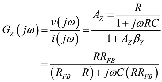 (4)
(4)
that for  (Gain = Losses condition) gives:
 (5)
(5)
Therefore, the Gain = Losses condition converts the lossy capacitor of capacitance C into a lossless one of the same C because this feedback in-phase with v(t) doesn’t vary C [5]. Using , the inverse Laplace transform of GZ(s) will be the time response of the system of Figure 2 to an impulsive driving current i(t) like those TAs occurring in C [4]. The GZ(s) of (5) indicates that a current impulse of weight q (a charge q displaced in C in a vanishing time interval) will set a voltage step
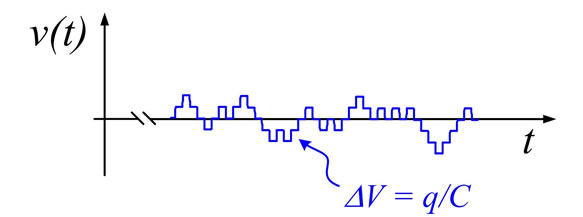
  V in C that will remain forever. These voltage steps appearing randomly in time and with random signs have been sketched in Figure 3 to show their null mean value
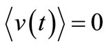 . Thus, this PF won’t “build” a voltage in C like the V0 we are looking for and moreover: the
  condition at each instant t can not be met because the random drift with time of R in this capacitor can’t be compensated for by the feedback network having its own, small drift with time.
To generate a noticeable voltage in C we need to have:
 or
or . This is the Gain > Losses condition meaning that (4) in s domain has a pole with positive real part (e.g.
  with
with ). In this case the steps of Figure 3 no longer are flat, but exponential risings. For the particular case
  (e.g
(e.g ), the resistance shunting C is:
  because
  and we obtain:
 (6)
(6)
Equation (6) means that an impulsive current of weight q will create a voltage  V in C that will rise exponentially with time constant
  for this particular βY. For
  pF and
  GΩ used previously we have:
  ms and a small voltage step
  nV growing in this way would reach 1 V in
  ms. For cuasi-dc signals as the aimed V0, this tstart seems a fast enough starting time that would be lower for higher βY values. Due to the random sign of the DRs (note that a DR is a voltage decay v(t) in Figure 4 coming from an impulsive current i(t) of one electron) we have to amplify only those DRs whose polarity is that of the aimed V0. This is done in Figure 4 by the rectifiers D1 and D2, taken as ideal ones to simplify. Due to the blocking action of D1, a voltage step
  V appearing in v(t) wouldn’t feedback current to the input whereas a positive
  would do it.
This positive ∆v would give a  rising with time as explained. Due to the blocking action of D2, a voltage
  wouldn’t feedback current, but for v(t) surpassing VRef, this NF loop will feedback a current iALC to counterbalance the excess of PF that existed during tstart, thus passing to sustain a voltage v(t) close to VRef, that the PF has “built” in C. Thus, this NF called Clamping Feedback (CF) is necessary to recover first and to keep continuously next, the
  condition that during tstart was:
  This CF implicit in the action of Automatic Level Control (ALC) systems or amplitude limiters used in oscillators, works when v(t) surpass VRef, thus generating the error signal it needs to be driven, which is
 .
.
When v(t) surpasses VRef, this CF has to feedback enough current to counterbalance the excess of PF used to start the system. With , the system starts with loop gain
  because
 . Note that the sign of –2/R in the PF generator of Figure 2 disappears if its arrow is reversed to follow the path allowed
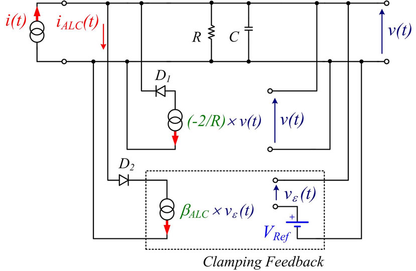
Figure 4. Electrical circuit with positive feedback and negative clamping feedback loops to generate first, and to sustain next, a positive voltage V0 in C (see text).
by D1. This βY shunting C by , needs to be counterbalanced in some extent by the CF when v(t) approaches VRef in order to leave C shunted by
  and by its own R. In this case the CF has to shunt C with a resistance
  to counterbalance the 50% of
  in order to recover the Gain = Losses condition or a loop gain
 . This requires a current
  coming from
 , not from v(t), thus meaning that the CF has to be very strong because it is driven by a signal of amplitude much smaller than the one it keeps in time, which is the output amplitude driving continuously the PF loop whose excess of feedback has to be counterbalanced by the CF.
Thus, any small signal as DRs (noise) appearing in v(t) when it is close to VRef will be strongly damped by this NF. If we define the Clamping Factor (CL) as:  we have:
 . Thus, the CF driven by vε(t) will be (CL + 1) times stronger than the PF driven by v(t) to feedback a similar current with regard the excess of PF that the CF has to counterbalance. This excess of PF is:
 (7)
(7)
that for  gives:
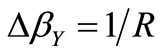 .
.
Since iALC(t) is generated from vε(t) that is (CL + 1) times lower than v(t) and it has to counterbalance a current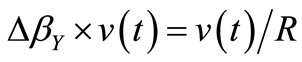 , the transconductance βALC thus required will be:
 (8)
(8)
Taking a 0.1% excess over VRef as error signal we have:
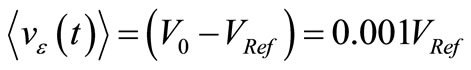 . In our particular case with
 , (8) gives
 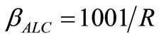 A/V. Thus, for small departures of v(t) from its mean value
 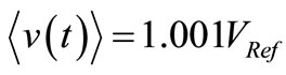 this CF will react as a resistance
  Ω shunting C. Since this reaction is driven by vε(t), any small voltage like noise added to its mean value
 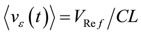 will feel this RDIF. For VRef = 1V the error signal driving the CF will be the dc signal
 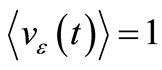 mV accompanied by the ac noise due to DRs being modified by the CF that dominates the circuit after tstart. Hence the reason to distinguish vε(t) from its average value (1 mV) that gives the conductance
 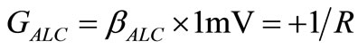 A/V that counterbalances at each instant the excess of PF used during tstart. Figure 5 shows the output voltage
  in our case, together with some DRs coming from TAs taking place in C, which would form the i(t) of Figure 4.
The CF is thus driven by a dc voltage  mV and by the ac noise of C, both feedback by βALC. The feedback of
 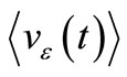 performs the aimed clamping function and the feedback of the noise changes its spectrum as shown by curve b) of Figure 6. For
  A/V, the low RDIF shunting C for
  means that the DRs of Figure 5 won’t decay with the native τ of Figure 1(b), but 1001 times faster. This is a known result coming from the Gain´Bandwidth product conservation in systems like this one where a flat NF is applied to a firstorder, low-pass, forward gain (see Chapter 5 of [11]). Since the rate λ of DRs is unaffected by this NF, the noise spectrum found in the voltage v(t) of Figure 4 will be that of curve b) of Figure 6, where the native spectrum of (3) has been broadened in frequency by
  and attenuated by
  due to the quadratic dependence of (2) with τ, because the amplitude
  of these “accelerated DRs” won’t change since C is not affected by this feedback in-phase [5]. Thus, the noise spectrum will be:
 (9)
(9)
whose ≈106 lower amplitude comes from the action of the CF on each DR, increasing its conduction current by 1001. Thus, this CF not only keeps the output amplitude close to VRef, but also damps heavily the noise it finds on the output amplitude in the form of DRs. A higher CL to

Figure 5. Detail of the voltage V0 = 1.001 V kept in C by the feedback system of Figure 4 together with its electrical noise (see text).
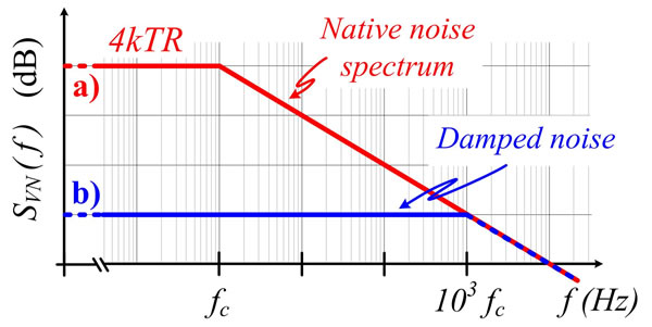
clamp v(t) more closely to VRef would give a higher attenuation and broader bandwidth in Figure 6(b), whence it can be found the reason for the name High Damping (HD) we will give to this effect due to the CF that underlies limiters and ALC systems of oscillators. This HD effect agrees with the action one expects for an ALC system that, unable to avoid the appearance of DRs in C, tries to remove them quickly once they have appeared.
It’s worth noting that this NF in-phase with v(t) = V0 is possible because we have a “resonator of ” whose output amplitude is a constant V0 allowing to consider that its output signal v(t) is at its top or with zerophase for this signal being:
  with
with . Despite its simplicity, this model gives a good picture about the way the CF will work in actual oscillators with f0 ≠ 0 that we will study in the subsequent paper under this same title. To pass from this “dc approach with
 ” to an ac one with f0 ≠ 0, we could discuss about the way to clamp negative semi periods in Figure 4 by adding a new feedback box with a third diode D3 injecting current towards the anode of D2 to allow an iALC(t) of opposed sense coming from a vε(t) of opposed polarity, obtained from the sampling of v(t) minus a VRef with proper sign. The two feedback boxes containing D2 and D3 would have to be driven by a time-varying reference signal
 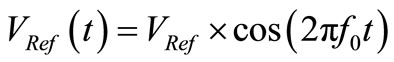 that they would use to clamp the output signal v(t) close to this VRef(t). The problem, however, is that this VRef(t) is not available because it requires to have in advance, at each instant of time, the signal the oscillator is going to generate. An approach to avoid this unavailable requirement is to sample the peak value of v(t) each period and to compare it with a dc reference VRef to generate the proper βALC to be used next. Although it works quite well, this approach has a drawback however, because it converts the ALC system or its implicit CF into a sampled system whose sampling rate f0 (or 2f0 by sampling the positive and negative peaks of the output signal), we will consider as appropriate in this introductory paper to simplify.
What we will study more carefully is the noise due to this solution that locks in phase the CF and the carrier of frequency f0 whose amplitude V0 it keeps in time close to VRef. We refer to the noise generated by this locked CF when it is confused by the noise it samples in quadrature with the carrier it tracks, because its heavy attenuation on the noise it samples in phase is clear from Figure 6 or by (9). To study this collateral effect that appears when the carrier has a non null frequency f0 ≠ 0, let’s consider that the NF of the ALC system or limiter is phase-locked to the carrier that is the big arrow (phasor) rotating at f0 times per second in Figure 7, where the noise coming from random DRs is the small arrow VN(t) at its end whose mean square voltage is  V2.
V2.
Since VN(t) points randomly respect to the carrier, we will consider its component along the carrier and that orthogonal to it. This endures a noise partition where the mean square voltage of noise sampled in-phase and that sampled in quadrature both are equal: kT/(2C) V2 and their sum is kT/C V2 (e.g. the sum in power of these two uncorrelated noises). With this partition, which acquires its proper meaning when phase can be defined for f0 ≠ 0 as we will see in actual oscillators, let’s redrawn Figure 6 where all the noise of C was sampled in-phase. This is shown in Figure 8 where curve a) is the noise spectrum of the resonator without feedback and where curve b) is the noise spectrum coming from the 50% noise of C being feedback in phase with the carrier, thus 3 dB less than curve b) of Figure 6. Concerning the +90˚ or –90˚ phase of the 50% noise power feedback in quadrature, let’s recall that the zero-phase reference is the current injected by the PF because it follows the amplitude of the carrier in oscillators of f0 ¹ 0. Because C stores energy as it builds voltage from the current it integrates in time, any noise current i(t) will create voltage components in v(t) at 0˚ (in-phase) and at –90˚ (in quadrature) respect to i(t) under SR. Since i(t) (Cause [4]) represents random TAs with any phase respect to the reference carrier, it will produce noise voltages (Effect [4]) both at –90˚ as well as at +90˚º in the error signal vε(t) driving the CF.
A noise voltage at –90˚ in the error signal vε(t) driving this NF means a current at –90˚ absorbed from the resonator following the arrow of iALC in Figure 4. This is equivalent to current at +90˚ arriving to the top node of the resonator that compensates current at +90˚ leaving it through C. Thus, DRs having in-quadrature components at –90˚ respect to the carrier being generated will find a lower capacitance than C (e.g. αC with α < 1) in the resonator due to this NF. This will give voltage steps of amplitude  with α times faster decay than those in TE without feedback, thus broadening their

Figure 7. Phasor Hz whose real part represents the output signal v(t) of an oscillator, disturbed by additive noise VN.
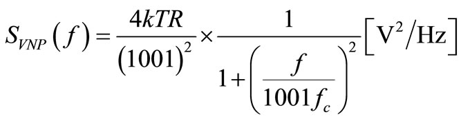
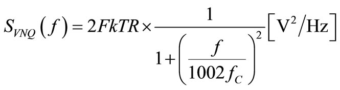
noise spectrum while keeping its amplitude as we wrote below (3). Dually, DRs with in-quadrature components at +90˚ respect to the carrier being generated, will find more capacitance than C in the resonator (e.g. αC with α > 1) thus giving a voltage steps of  V with α times slower decay than those in TE without feedback. This will narrow their noise spectrum while keeping unaffected its amplitude because none of these feedbacks in quadrature modifies R [5]. Hence, the CF confused by noise in-quadrature will broaden the native noise spectrum while keeping its 2kTFR V2/Hz amplitude and this will give a noise Pedestal of 2kTFR V2/Hz due to the 50% noise power the CF finds in quadrature.
To compare this noise with its corresponding noise sampled in phase, curve b) of Figure 8, let’s take a feedback factor of equal magnitude to the one we have used for curve b): , for j being the imaginary unit meaning +90˚ phase shift. Let’s take a resonator with
  where the current through C at f0 is 1002 times higher than that through R. In this case, the
 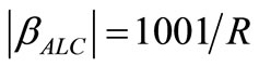 A/V of the CF would compensate 1001 parts of the 1002 parts of current flowing through C at f0.
Although this reasoning in SR requires an f0 ≠ 0, let’s continue as if currents in the resonator had a non null  allowing the aforesaid noise partition. The capacitive current at
  demanded by the resonator with this feedback would be only 1/1002 times the current of C, while its R would be unaffected. Thus, each DR of
  V amplitude and time constant τ in TE would pass to have amplitude 1002(
 ) V and time constant
 . The spectrum of these DRs sampled and feedback in quadrature would have ≈1000 times higher bandwidth but the same amplitude 2kTFR V2/Hz of the 50% noise spectrum found in quadrature by the CF, as it is shown by curve c) in Figure 8. It would be:
 (10)
(10)
where the 2 below the Johnson noise 4kTR V2/Hz recalls

Figure 8. (a) Noise spectrum of C in TE; (b) Damped noise created by the CF from noise sampled in-phase; (c) Pedestal of noise from noise sampled in quadrature by the CF.
the orthogonal partition of the noise in C. Following [4], an equivalent Noise Figure F like that of [7] means that the rate λ of TAs and DRs is F times higher than the average rate  of thermal TAs associated to R in TE at T. If the resonator of
  we are using had a temperature
  due to the power it is Converting into heat (
 watts in dc, see next section), the extra noise due to
  and the noise added by the feedback electronics could be taken into account by the Noise Figure F of [7]. In this case, the noise Pedestal becomes:
 (11)
(11)
Given the difficulty to handle the in-quadrature term of a signal of , we won’t go further with this reasoning, thus leaving (11) as a good reason to find a broad Pedestal of electrical noise at 2FkTR V2/Hz added to the carrier whose amplitude is kept in time by a CF that becomes synchronous with it. This Pedestal is the collateral effect of thermal noise sampled in-quadrature by the feedback electronics governing the ALC system of oscillators. This Pedestal shown by curve c) of Figure 8 represents more noise power than the 50% noise power sampled in-quadrature because the Clamping Feedback reduces the noise it samples in-phase as shown by curve b) of Figure 8, but enhances the noise it finds with phase error of –90˚, because it lacks the right phase to be negatively feedback. Updating (9) with
  and this noise partition we have:
 (12)
(12)
Since this mix of discrete noise, electronic feedback and noise partition can be hard to be accepted at first sight, we will give added proofs by PSPICE that can be refined at the expenses of a higher computational cost or by other simulation tools. Figure 9(a) shows the Lorentzian noise spectrum that appears when a discrete and pseudo-random noise current mimicking the noise model of [4] drives the resonator of  of Figure 9(b) formed by a capacitor of 10 pF whose losses are represented by 10 GΩ. To have unambiguous results, TAs displacing
  C each in [4], have been replaced by big TAs, each displacing a charge packet
  C by a current pulse of 10–9 A height and 0.1 ms width, whose appearance in time is each 2.1 ms, with random sign to give a rough emulation of thermal noise in the resonator of Figure 9(b) where it is injected through the transconductance generator G1. Thus, we have a pulsed “noise current” of
  duty cycle and
 (a)
(a)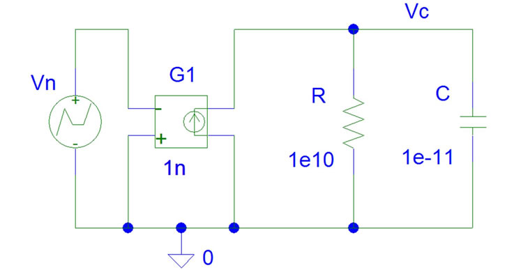 (b)
(b)
Figure 9. (a) Native noise spectrum of the circuit of Figure 9(b) driven by the charge noise described in the text. (b) Circuit of a capacitor of capacitance C and losses represented by R, driven by a charge noise (see text).
fixed rate 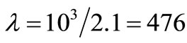 s–1 (a Pseudo-Random Noise PRN) to emulate the thermal charge noise power of
 [4] in
  pF shunted by
  GΩ .
GΩ .
This power or “Nyquist noise density 4kT/R A2/Hz on R” is: 1.7 ´ 10–30  (or A2/Hz) at room T, whereas the power of the PRN is:
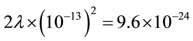 (or A2/Hz), the factor 2 coming from the fact that each “fat TA” or fast displacement of a charge qbig in C, triggers a “fat DR” or slower displacement of charge –qbig (an opposed displacement) to Dissipate the energy stored by the fat TA, thus doubling the charge noise power of λ “fat TAs” per unit time taking place in C, as it happens with the TA-DR or Cause-Effect pairs in [4]. The higher power of the PRN respect to
  avoids resolution problems with non ideal rectifiers (see below). On the other hand, the average rate
 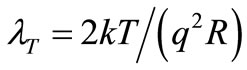 of true TAs in this resonator of
  would be:
  s–1 whereas the PRN has a fixed rate λ that roughly is 7 ´ 104 times lower than λT. Thus, the ≈106 times higher charge noise power of the PRN comes from the “fat electrons” (each of charge –qbig) that it uses to emulate electrical noise in an Admittance accordingly to [4].
Figure 9(b) shows the PSPICE circuit used to inject this pulsed PRN into the R-C resonator in order to create the voltage noise on C that will emulate Johnson noise in this resonator of . Considering that each qbig shifts the voltage VC in C by
 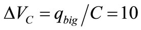 mV and that the time constant of the subsequent decay is:
  s, we can use these values and (2) multiplied by
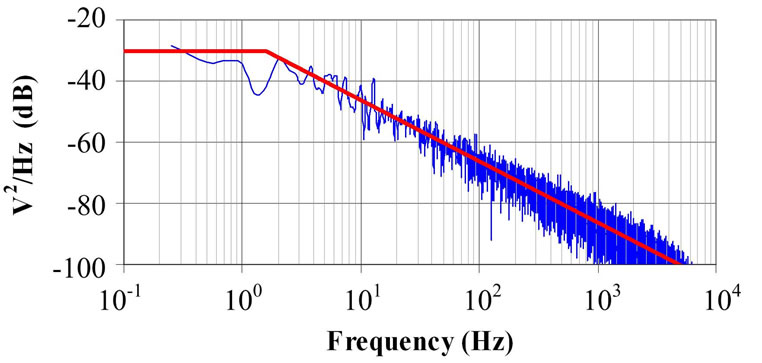
  s–1 to predict the spectrum of this PRN in VC. This way the flat region of the Lorentzian shown in Figure 9(a) would be: 2 ´ 476 ´ 10–6 V2/Hz (e.g. –30 dB), thus agreeing well with the FFT of the VC-time series given by PSPICE in the circuit of Figure 9(b). This same value appears by converting A2/Hz into V2/Hz through the square of the Resistance where the Nyquist noise (in A2/Hz) “is being applied”. Multiplying 9.6 ´ 10–24 A2/Hz by
  Ω2, we have: 9.6 ´ 10–4 V2/Hz, as expected. The two asymptotes drawn in Figure 9(a) show the cut-off frequency
  Hz of this spectrum, as it must be for this τ of 0.1 s. This PRN is the charge noise driving continuously the resonator during the simulations to come.
Figure 10 shows the PSPICE circuit that simulates the “oscillator of ” proposed in Figure 4 to build a dc voltage V0 in C. Its dc reference VRef leads to build a VC voltage on C close to 3 V. The voltage amplifier E1 of

Figure 10. Positive feedback and CF loops used to build and to sustain next a voltage V0 in the resonator of Figure 9(b).
gain 104 V/V driving the diode D, followed by the amplifier E2 of inverse gain 10–4 V/V allows to rectify small voltage signals in VC as if the diode D (model 1N4007) had a turn-on voltage of  μV, thus negligible for the voltage steps
  mV created in C by each charge packet qbig of the PRN. This way, the first positive ∆VC on C will appear at the output of E2 with amplitude
  mV due to the precision rectifier that form E1, D, R1 and E2. This ∆VCfirst will be positively feedback to the input through the transconductance amplifier of gain
  A/V that is 2 times the –1/R gain required to compensate resonator losses represented by its
  GΩ. Thus, the loop starts with
 , the same value we used to describe Figure 4. Since any
  mV is blocked by D, only positive voltage is built in C during the starting time tstart. When VC(t) reaches 2.9 V, switch S closes to activate the CF accomplished by the amplifier of gain
  A/V, whose 25 times higher gain than Gp leads to a clamping factor:
  (e.g. to counterbalance the excess of PF we have in Gp driven by
  V, a signal
  V has to drive Gn in steady state). PSPICE shows that starting from
 , a voltage
  V appears in tstart≈15 ms and shortly after we have
 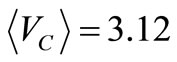 V.
V.
We distinguish  from VC because the 10 mV peaks due to the fat TAs of the PRN driving continuously the circuit appear onto
  as PSPICE shows. To have a resolution better than 0.25 Hz, transient simulations lasting more than 4 seconds have been used while the PRN is being injected. The first 0.02 seconds corresponding to tstart in the VC-time series of data given by PSPICE were not used to be in “steady state” (e.g. after tstart). The voltage on C in steady state mimics Figure 5, being formed by a dc value
  V plus the ac voltage noise due to the PRN, both governed by the CF. The error signal driving the CF is thus:
  where vac represents these
  mV noise decays that form the noise viewed by the CF. It’s worth noting that in steady state, these noise decays are feedback with gain ≈ 1 because for
  V, a dc current
  mA flows through diode D. With this dc bias, D converts ≈0.7 mW into heat and does not rectify at all the small noise decays
  mV that are added to
 . Instead, it offers a dynamical resistance rd = VT/ID ≈ 25 Ω allowing their passage to R1 with negligible attenuation (e.g. one part per million). This way, the decays of noise with amplitude ±10 mV in C are transferred with unity gain to the output of E2 and feedback through Gp and Gn. Due to the simplicity of this circuit, R1 converts into heat 32 W in steady state, although this is irrelevant for the results.
Figure 11(a) is the spectrum of the signal that exists on C in Figure 10. Using  in (8) and (9), the native noise spectrum of Figure 9(a) would be attenuated by
  (e.g. 28 dB less) whereas its cut-off frequency would be 26 times the fC of Figure 9(a). Thus, the noise on C would be a Lorentzian at –58 dB with its cut-off at
  Hz that agrees well with the FFT of the VC(t)-t series that PSPICE gives for the circuit of Figure 10. This is the spectrum under the dashed line drawn to guide the eye in Figure 11(a).
Since this spectrum merges at high frequencies with the upper Lorentzian that repeats the asymptotic spectrum of Figure 9(a), we confirm that for noise being feedback in phase, the G × BW product is conserved, as predicted.
Given the agreement between these simulations and our theory for the noise the CF “sees” in phase, let’s try to find some proof concerning noise it sees in quadrature. The first point to consider is that for a signal like VC(t) that mostly is a dc signal of , we would have to wait an infinite time to pass from phase 0˚ to phase –90˚, but this is not so for its small ac components. Although we could synchronize its feedbacks with a carrier of frequency fx. and use a signal in quadrature with fx to build the feedback of noise in quadrature, this would modify the circuit in such a way that the results would be obscured by the extra knowledge required to handle the electronics. Thus, we will give a partial proof (only in a frequency band) about the effect we expect from a CF seeing noise in quadrature that is: a noise Pedestal of density 2FkTR V2/Hz. Since we need a CF working around the resonator, let’s use that of Figure 10 that clamps perfectly the amplitude to the designed value of 3.12 V. Hence, Figure 12 is the circuit of Figure 10 with an added path to feedback the ac voltage on C multiplied by –j. This feedback at –90˚ is done by converting the ac
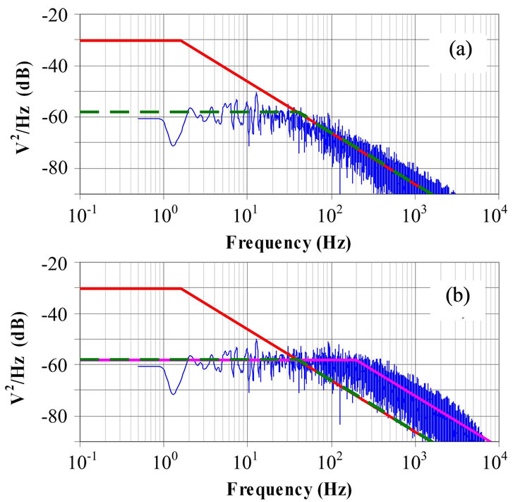
Figure 11. (a) Noise spectrum of the capacitor of Figure 9(b) under the feedbacks of Figure 10; (b) Noise spectrum of the same capacitor with the feedbacks of Figure 12 (see text).
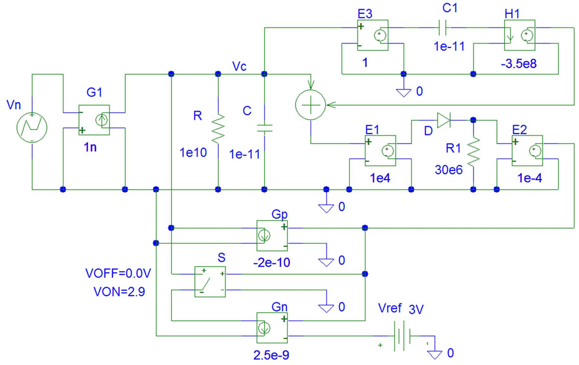
Figure 12. Electrical circuit of Figure 10 with an added path in the Negative Clamping feedback to feedback noise in quadrature as described in the text.
voltage in C into an ac current through C1 whose Fourier components will be at +90˚ respect to the Fourier ones of this ac voltage because displacement currents in C1 come from the time derivative of each voltage component on C1. This current at +90˚ respect to voltage on C is converted into a new voltage by the transimpedance amplifier of gain H1 whose negative sign gives the –90˚ phase lag we are looking for.
As Figure 12 shows, the ac voltage on C and this new voltage in-quadrature are added to drive the circuit that, being a precision rectifier during tstart, becomes a unity gain circuit feeding back the resonator in steady state as explained. Setting H1 = 0, the circuit of Figure 12 becomes that of Figure 10 and the spectrum of voltage noise that appears in C is that of Figure 11(a). Since the feedback in phase of the CF has to exist continuously, (otherwise we wouldn’t have a CF liable to feedback something in quadrature) and this already generates the noise spectrum of Figure 11(a), this spectrum has to be viewed as the native spectrum of noise the feedback in quadrature finds when it is born by setting the gain of H1 to a non null value. Therefore, any change in the spectrum of noise on C coming from the CF mislead by noise in quadrature, has to be referred to Figure 11(a). For readers worried about this double feedback through the adder of Figure 12 we will say that after tstart (when the E1, D, R1, E2 block becomes a linear, unity gain amplifier) it works perfectly because the orthogonal signals it handles do not merge, a feature used in [5] to handle the phase error in the loop gain of oscillators and its induced (Technical) phase noise. As the gain of H1 is increased, the amplitude of the noise peaks on C increases while their decay becomes faster. For H1 = –3.5 ´ 108 V/A, this amplitude roughly is five times higher than for H1 = 0 and the noise peaks decay five times faster.
Thus, this noise viewed in quadrature by the CF would be finding a capacitance ≈C/5 in the resonator. The FFT of the VC(t)-time series PSPICE provides for the circuit of Figure 12 gives the spectrum of Figure 11(b), thus with the same amplitude but roughly 5 times larger bandwidth than the native noise of Figure 11(a). The rather large gain we use in H1 is to compensate the low voltage-current conversion gain we have previously due to the small value of C1. The overall value of these gains: , depends on frequency because the +90˚ phase shifter we had to use is not the differentiator we have used, where the amplitude of its output signal rises with f. With a –90˚ phase shifter of flat response we could do a better simulation, but this would complicate more than clarify the circuit. Therefore we will say that Figure 11(b) shows the trend of the CF to create a Pedestal of electrical noise in the resonator when it is mislead by noise in quadrature. The gain βQuad(f) in the circuit of Figure 12 that is unity around
  Hz, thus near the frequency
  Hz of Figure 11(a), means that this feedback of noise at –90˚ and that of noise in-phase are of similar strength around fCclamp, where the native noise spectrum had dropped 3 dB in Figure 11(a). However, the noise spectrum recovers its flat or low-f value around fClamp as Figure 11(b) shows, thus meaning that this CF in quadrature tends to sustain the native noise amplitude when its magnitude is similar to that of the feedback in phase. This proves quite convincingly the generation of a Pedestal of 2FkTR V2/Hz amplitude by the CF confused by a noise density of 2FkTR V2/Hz that it will find in quadrature with the carrier in oscillators with f0 ¹ 0.
It is worth noting that the noise we have considered in TE (V0 = 0) and out of TE with V0 ¹ 0 has been the same despite the very different electrical power linked with R in TE and out of TE. We mean that the noise power Dissipated by R in TE is kT/(RC) W following [4] whereas the power handled by R,  W out of TE, can be millions of times larger. If neither the rate λT of DRs nor the energy
  Dissipated by each DR [4] are changed by the feedbacks, two questions that are essential to understand Phase noise in oscillators arise: 1) what happens with the instantaneous power pi(t) that the feedback generators inject continuously to sustain V0 ¹ 0?. And 2) How does this pi(t) affect the TA-DR pairs of events [4] or the Fluctuation-Dissipation phenomena [12] that underlie electrical noise?. Next Section considers these questions.
3. Dissipation of Energy and Conversion of Energy into Heat
The Signal power pi(t) W that enters the resonator in electrical form to sustain its V0 uses to be considered as power dissipated in R that heats the resonator. Since Dissipation was linked to Fluctuation long time ago in a Quantum treatment of noise [12], we prefer to say: “the power pi(t) that enters the resonator in electrical form is equal to the power that leaves it converted into heat”. This unbinds pi(t) from each Dissipation of electrical energy started by its previous Fluctuation in the Admittance where electrical noise appears [4]. This distinction is needed because if pi(t) was Dissipated in the same way each energy Fluctuation is, it would affect strongly the observed noise and this is not so. We refer to the noise of a resistor in TE with its R Dissipating 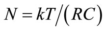 W by
W by  V2 driving its R and to the noise of this resistor absorbing millions of times this power under V0 ¹ 0, thus out of TE, that are similar when the heating effect is low. Using the Admittance of Figure 1(a) as a cogent circuit for their electrical noise [4], this noise comes from a random series of (TA-DR) pairs of events occurring in C at this average rate [4]:
 (13)
(13)
where  is the thermal voltage.
Conductance is thus a rate of chances in time to Dissipate electrical energy in TE, each involving the elemental charge unit q. Since C is the direct transducer converting kinetic or thermal energy of carriers into electrical one [4], let’s find the inverse transducer that converts electrical energy entering the resistor into disordered energy observed as heat. Considering that the thermal noise of a resistor doesn’t vary noticeably when a dc current is allowed to flow provided its heating effect is low, we can find that the inverse transducer also is a capacitance Cf, quite different from C. To have some figures, let’s consider a resistor of R = 1 MΩ shunted by  pF under open-circuit conditions. Integrating (3) from
  to
to , the mean square voltage on R at T = 300 K is:
  V2 (e.g. 100 μVrms or the well known kT/C noise of C). This voltage generated in C that is driving R means that the mean noise power Dissipated by R is:
  W in TE at 300 K. Injecting a dc current Idc = 1 μA to this resistor, a dc voltage between terminals Vdc = 1 V will appear and the electrical power entering this resistor out of TE will be: S = 1 µW. For a macroscopic resistor with dimensions in the mm range, this Signal power S won’t rise noticeably its T. Thus, the noise in TE at T with R Dissipating N watts and the noise out of TE with R “handling” S = 108N at T* ≈ T, will be quite the same as one finds measuring noise in resistors. This similarity in spite of the 100 millions factor of the power handled by R suggests that the Dissipations of energy in TE [4] and those converting pi(t) into the heat power that appears in the device, are different. Thus we have to look for a way to convert pi(t) into heat while keeping its electrical noise for T* ≈ T. Following [4], this requires to conserve λT with V0 ¹ 0, to keep the average number of electronic charges arriving at the terminals (or plates) of the resistor. Since pi(t) is G = 1/R times
 , a way to convert pi(t) into heat with this
  dependence is by loading each carrier arriving to a plate with an energy proportional to
  as if each carrier giving noise had a capacitance Cf driven by V0. The word loading means that each carrier has to offer a reactive behaviour to V0, like a capacitive Susceptance able to store electrical energy taken from V0. This energy loaded onto the carrier would be released to the terminal (Collector) where the aforesaid carrier was captured.
In a device made from two plates at temperature T separated by a distance d in vacuum (an R-C cell studied in [1]), a reactive behaviour could be expected from the mass (inertia) of free electrons accelerated by the electric field . This way, an electron emitted with kinetic energy Ui from the negative plate (cathode) would reach the anode with total energy
  J. The displacement current that began when it left the cathode would cease at its arrival to the anode and this would store a Fluctuation of
  J in C due to the charge q displaced between its plates. This is an energy stored by the device in its susceptance between terminals, thus able to drive the subsequent DR in TE that is what we call Dissipation in [4] to agree with the Fluctuation-Dissipation of energy studied in [12]. Without other ways to store energy between terminal, the excess of energy brought by the carrier:
 , will be released to the Collector plate by phonons, thus as heat. Therefore the fast Fluctuations of energy (TAs) creating electrical noise in a device would be the energy packets it stores in electrical form each time an elemental charge is displaced between its two terminals and only this energy is Dissipated after each Fluctuation accordingly to the TA-DR or Cause-Effect dynamics of [4] and the extra energy surpassing ∆U is Converted into heat.
This difference between energy Dissipated and that Converted into heat is clear in this vacuum device, where the power converted into heat would be, however, proportional to V0, not to  (at least for
 ). This means that kinetic energy acquired by charges like electrons in vacuum doesn’t give the reactive behaviour we are looking for, but this will be different in Solid State devices, whose free carriers in bulk regions between two terminals tend to bear charge neutrality by two opposed charges screening one to each other. The average number lT of electrons per second reaching the two plates or terminals of the two-terminal device (2TD) like a resistor or capacitor one has to build to measure Johnson noise is given by (13). These 2TD can be made small (e.g. differential) and repeated many times if necessary (e.g. connected in series or parallel) to study noise within a macroscopic device for example, but its 2TD character never is lost because the electrical noise “of a material” hardly will be measured. Only the noise of a device made from this material can be measured, but this device can produce its own noises like those of [1,2] that become puzzling when they are assigned to the material and not to the device that produces them. For a resistor made of n-type semiconductor, free carriers for electrical conduction are electrons in the Conduction Band (CB) whose name “free electrons” as opposed to trapped ones, does not mean “free electrons in vacuum”.
An electron in a quantum state (QS) of the CB has a extended wavefunction within the device that “connects” its two terminals in the sense that one terminal can emit an electron to this QS as soon as it is left empty by the other terminal having captured the electron that was previously in this QS, being this a mechanism allowing the TAs of [4]. Since the electrical noise observed in a resistor in TE and when it conducts a dc current Idc is quite the same provided heating effects are small, we have to keep lT while conducting Idc. On the other hand, to convert electrical energy taken from the applied V0 into heat as Joule effect requires, a starting point is to look for a way to load each carrier with energy proportional to  or for a way to convert each carrier into an electrically reactive element sensing V0 and storing an energy proportional to
  as a Susceptance driven by V0 would do. This leads to consider the electrical structure of an electron in the CB as formed by a mobile cloud of charge –q screening its corresponding positive charge +q that would be a sort of fixed density of charge distributed in the volume of the resistor, both depending on lattice atoms, defects, etc. as well as on the Bloch functions that define the wavefunction of this electron within the solid matter of the device. What matters is to realize that a “free carrier” in the CB is not a charged particle like an electron in vacuum, but a neutral charge structure to keep charge neutrality in the bulk region we are considering between terminals.
For an electron emitted to the lowest energy level or QS of the CB at , the first “image” of its associated charge density would be one with the –q cloud of charge wrapping closely its corresponding +q charge array, thus with a good screening at each spatial point within the resistor. This picture would correspond to a carrier very “cold”, not yet in TE with its surrounding universe. It’s easy to realize that this carrier can store electrical energy or has a Degree of Freedom to do it by changing the average screening between its –q charge cloud and its +q charge array. Thus, it will interact thermally with its environment by energy exchanges leading it to hold an average thermal energy of kT/2 J in the form of an average, non-perfect screening between the aforesaid +q and –q charges densities, a screening fluctuating randomly in time due to thermal activity. Using the quantization of the electrical charge no matter its spatial distribution in a QS of the CB, each free electron in the CB reacting as a sort of capacitance Cf with opposed charges +q and –q on its plates, would be an energy carrier liable to load electrical energy from the electric field sustained by the external generator of current Idc that sets V0 ≠ 0 between terminals. Using Equipartition for this Degree of Freedom as we did for C in [4], the average capacitance Cf that thermal activity will set in each free electron of the CB will be obtained by equating the energy stored by this reactive Degree of Freedom:
  to the thermal energy per degree of freedom kT/2. This gives:
 (14)
(14)
Equation (14) that we have obtained here in TE after having presented Cf, was first obtained as a way to extract the electrical power pi(t) from the resistor body without varying its noise, thus keeping λT. Assuming that the λT electrons per second reaching the contacts of the resistor were responsible for this extraction, the energy Uf that each electron had to bring was:
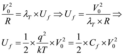 (15)
(15)
an equation suggesting that this extraction was accomplished by electrons of charge q reaching the contacts thermally, but previously loaded with an energy Uf taken from V0 as if they were capacitances Cf sensing V0. From this idea, the meaning of Cf expressed by Equation (14) was obtained and the conversion of electrical energy from the external generator into heat was separated from the Dissipations associated to Fluctuations.
Therefore, when a free carrier of the CB leaves this band to appear as a charge –q on the contact where it is collected, it stores an energy Fluctuation ∆U in C (cause) subsequently Dissipated by the DR it produces (effect) [4]. This produces the electrical noise observed in TE and out of TE provided the heating effect is low . Out of TE, however, any energy brought by the free carrier in excess of ∆U, like Uf in Solid-State devices or kinetic energy of electrons moving in vacuum, can’t be stored in C as a Fluctuation of electrical energy, thus being converted into heat. The noise power of a resistor in TE:
  W is Dissipated accordingly to the Fluctuation-Dissipation Theorem derived from [12], but the electrical power S = pi(t) entering the device out of TE is Converted into heat as explained. The loading of Cf with Uf or the passage of a carrier in the bottom of the CB to a level of higher energy, involve fluctuations of energy that, not being stored by the device (e.g. in its C) are not Fluctuations of energy liable to produce Dissipations in the sense of [4,12]. This distinction between Dissipation and Conversion is essential to understand Phase Noise in actual oscillators.
4. Conclusions
When a voltage v(t) coming from positive feedback of v(t) itself is clamped to a value close to a reference VRef, a NF called Clamping Feedback driven by an error signal vε appears. This way, the output voltage becomes: V0 = VRef + vε and since , this negative feedback is very strong for vε and its added noise. The action of this NF on small signals like noise added to the output amplitude is thus a High Damping effect aiming to remove them quickly. Due to this effect, the Dissipation of electrical energy that each DR carries out is accelerated, thus producing attenuation and broadening of the native noise spectrum so as to conserve the Gain×Bandwidth product. This situation coming from feedbacks at 0˚ and 180˚, no longer holds when this NF becomes phase-locked to a carrier whose amplitude it has to keep in time. In this case, this Clamping Feedback finds 50% of noise power in-phase and 50% noise power in quadrature. Whereas the noise in phase is heavily damped as explained, the noise in quadrature confuses the Clamping Feedback in such a way that creates the Pedestal of electrical noise that appears in systems like Automatic Level Control and amplitude limiters used in electronic oscillators. Concerning the electrical power (Signal power) that enters a resonator where a voltage V0 is sustained in time by any means, it is Converted into heat without affecting its noise provided its heating effect is low. This will be quite the case for High-Q resonators whose small heating effect will be accounted for easily by the effective Noise Figure F of the oscillator loop.
REFERENCES
- J. I. Izpura, “On the Electrical Origin of Flicker Noise in Vacuum Devices,” IEEE Transactions on Instrumentation and Measurement, Vol. 58, No. 10, 2009, pp. 3592- 3601. doi:10.1109/TIM.2009.2018692
- J. I. Izpura, “1/f Electrical Noise in Planar Resistors: The Joint Effect of a Backgating Noise and an Instrumental Disturbance,” IEEE Transactions on Instrumentation and Measurement, Vol. 57, No. 3, 2008, pp. 509-517. doi:10.1109/TIM.2007.911642
- H. Nyquist, “Thermal Agitation of Electric Charge in Conductors,” Physical Review, Vol. 32, 1928, pp. 110- 113. doi:10.1103/PhysRev.32.110
- J. I. Izpura, J. Malo, “A Fluctuation-Dissipation Model for Electrical Noise,” Circuits and Systems, Vol. 2, No. 3, 2011, pp. 112-120. doi:10.4236/cs.2011.23017
- J. Malo and J. I. Izpura, “Feedback-Induced Phase Noise in Microcantilever-Based Oscillators,” Sensors and Actuators A, Vol. 155, No. 1, 2009, pp. 188-194. doi:10.1016/j.sna.2009.08.001
- J. Malo and J. I. Izpura, “Feedback-Induced Phase Noise in Resonator-Based Oscillators,” Proceedings of DCIS’09 Conference, Zaragoza, November 2009, pp. 231-236. http://www.linkpdf.com/ebook-viewer.php?url=http://dcis2009.unizar.es/FILES/CR2/p5.pdf
- D. B. Leeson, “A Simple Model of Feedback Oscillator Noise Spectrum,” Proceedings of IEEE, Vol. 54, 1966, pp. 329-330. doi:10.1109/PROC.1966.4682
- D. Ham and A. Hajimiri, “Virtual Damping and Einstein Relation in Oscillators,” IEEE Journal of Solid-State Circuits, Vol. 38, No. 3, 2003, pp. 407-418. doi:10.1109/JSSC.2002.808283
- A. Hajimiri and T. H. Lee, “A General Theory of Phase Noise in Electrical Oscillators,” IEEE Journal of SolidState Circuits, Vol. 33, No. 2, 1998, pp. 179-194. doi:10.1109/4.658619
- T. H. Lee and A. Hajimiri, “Oscillator Phase Noise: A Tutorial,” IEEE Journal of Solid-State Circuits, Vol. 35, No. 3, 2000, pp. 326-336. doi:10.1109/4.826814
- http://www.ti.com/lit/an/slod006b/slod006b.pdf
- H. B. Callen and T. A. Welton, “Irreversibility and Generalized Noise,” Physical Review, Vol. 83, No. 1, 1951, pp. 34-40. doi:10.1103/PhysRev.83.34
NOTES
*Work supported by the Spanish CICYT under the MAT2010-18933 project, by the Comunidad Autónoma de Madrid through its IV-PRICIT Program, and by the European Regional Development Fund (FEDER).