Journal of Modern Physics
Vol.5 No.1(2014), Article ID:42259,4 pages DOI:10.4236/jmp.2014.51008
Long-Time Relaxation and Residual Conductivity in GaP Irradiated by High-Energy Electrons
A. Alikhanian National Science Laboratory, Yerevan Physics Institute, Yerevan, Armenia
Email: *grant@mail.yerphi.am
Received November 11, 2013; revised December 9, 2013; accepted January 5, 2014
ABSTRACT
This paper presents the results of a study of long-time relaxation (LR) and residual conductivity in n-type gallium phosphide (GaP) crystals irradiated by 50 MeV electrons. A manifold increase in photosensitivity and quenching of residual conductivity was found as a result of irradiation. It is shown that LR in GaP is due to disordered regions (generated by electron irradiation) which have conductivity close to self one. The Fermi level in the disordered regions is determined by which is located deep in the forbidden band (Ее − 1.0 eV). LR effect is mainly explained by a spatial separation of electrons and holes, recombination of which is prevented by potential barriers. The observed increase in conductivity is associated with the increase in the concentration of minority carriers as well as with increase of the Hall mobility at the sample illumination.
Keywords:Long-Time Relaxation (LR); Residual Conductivity (RC); Photoconductivity; Irradiation; Gallium Phosphide
1. Introduction
There are a lot of publications on anomalously large relaxation time of photoexcited carriers in a variety of materials, especially in semiconductors. A review of extensive experimental data accumulated by now has enabled to formulate some general patterns [1]. At present, there are two models to explain the phenomenon of long-time relaxation (LR) and residual conductivity (RC) in inhomogeneous materials. One of them is based on the idea of capturing non-equilibrium carriers by strongly localized states in the vicinity of point defects or impurities with deep energy levels. Another is a barrier model, which includes spatial heterogeneities in the vicinity of clusters, the defects generated by irradiation with heavy ions, neutrons or fast electrons. Both models are complementary and closely related to each other, allowing qualitative interpretation of the observed experimental results on LR and RC. The data presented in papers [2-6] devoted to the nonequilibrium photoconductivity of irradiated or S-doped AIIIBV semiconductor compounds, can be used to reveal the mechanisms resulted in LR and the states with RC.
Gallium phosphide is one of the main optoelectronic materials. The increase in photosensitivity is of great practical importance when manufacturing devices on it basis.
This article presents some results on the increase of photosensitivity of GaP samples irradiated by highenergy electrons as well as an analysis of the experimental data obtained when investigating photoconductivity and RC after turning of photoionization.
2. Experimental
The measurement of spectral dependence of photoconductivity was carried out at 300 K and 80 K at constant illumination using the SF-8 spectrophotometer’s monochromator (Russian production). Figure 1 shows the measurement scheme.
A sample r at the monochromator output is illuminated constantly. Signals v from the loading resistance Rн come to electrometer and then recorded by PC. The maximum value of v can be achieved by proper selection of Rн. For
 and
and , it was obtained
 (i.e. v is proportional to the relative change of conductivity, ∆σ when illuminated). In this expression rо, σо are the sample resistance and conductivity in the dark, respectively, V is voltage (not more than 5 V) applied to the sample.
Tellurium doped n-type GaP samples with initial concentration of ~1017 cm−3 had ohmic contacts obtained by fusing of pure indium into the sample at 500˚C during 5 minutes at the nitrogen environment. The samples were irradiated by 50 MeV energy electrons at current density 1 mkА·cm−2 and the temperature not higher than 20˚C.
3. Results
Figure 2 shows the spectral distribution of photoconductivity of irradiated n-GaP crystals. It is seen that photoconductivity appears at photon energy of 1.0 eV, then it increases monotonously, at hn > 2.2 eV it rises sharply and then decreases sharply beginning from ~2.4 - 2.5 eV. A similar pattern occurs at the measurement temperature of 80 K.
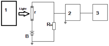
Figure 1. 1—SF-8 spectrophotometer, 2—electrometric amplifier, 3—PC, r—sample, B—battery.
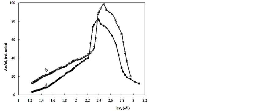
Figure 2. Spectral dependence of photoconductivity at 300 K (curve a) and 80 K (curve b) for n-GaP crystal irradiated by 50 MeV electrons at a dose of 2·1016 e/cm2.
Note, that the original crystals were almost not photosensitive, and just during irradiation their photosensitivity increased sharply, thus increasing the relative photoconductivity signal,  , where I is the excitation light power. The nonstructured nature of the spectral curve of impurity photoconductivity (from 1 eV to 2.2 eV) is associated with the presence of disordered regions in irradiated gallium phosphide.
It is known [7,8] that the disordered regions are some parts of the whole semiconductor volume with high concentration (~1019 cm−3) of radiation-induced defects and allowed states (occupied by electrons or free of them, depending on the Fermi levels in there) forming nearly continuous spectrum in the band gap.
The disordered regions can contribute to the photoconductivity, if the non-equilibrium carriers, excited in them by light, are able to escape from their bounds during their lifetime (which varies within the range of 10−9 - 10−2 s). The average displacement of non-equilibrium carriers due to diffusion calculated by Einstein formula is 1000 Å, which is much larger than the average radius of disordered regions (hundreds of angstroms, according to assessments). So it would appear reasonable that there is a spatial separation of light-excited electrons and holes, recombination of which is prevented by potential barriers. They easily leave the bounds of the disordered regions and contribute to the photoconductivity. The observed both LR in the whole spectral range of photosensitivity of irradiated crystals and RC after turning off the light, confirm this assumption.
The curves of photoconductivity relaxation at 300 K and 80 K presented in Figure 3 testify to the fact that after switching off the photoactive light, the sample transforms into a state with residual conductivity.
Let us consider the results obtained when investigating the RC quenching. The quenching occurs, when an electron in the potential well receives the energy required to overcome the recombination barrier [1,9]. When irradiated by 50 MeV electrons, such recombination barriers are created by disordered regions. As can be seen from Figure 3, quenching occurs when illuminated with light wavelength of λ = 1.24 mkm (if illuminated with λ > 1.24 mkm, RC does not change), which gives hν = 1.0 eV as the maximum height of the potential barrier of disordering. In addition, it follows from Figure 2 that the longwavelength limit of photosensitivity at 300K, determined by the position of Fermi level in the disordered region, is close to hν = 1.0 eV. In otherwise, for the RC quenching it is necessary for main carriers located at the bottom of the potential pit to receive an energy higher than 1eV (λ = 1.24 mkm)—the height of potential barrier of disordered regions. At illumination by light of λ = 1.3 mkm wavelength, the photon energy is not enough for over
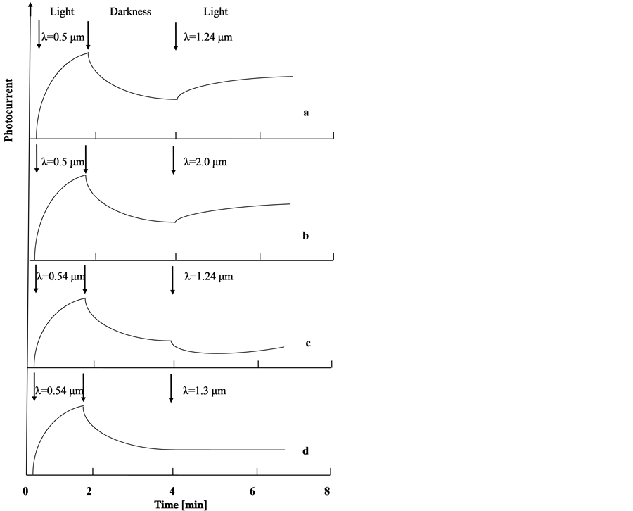
Figure 3. The photocurrent relaxation curves for the irradiated n-GaP at 300 K (curves a, b) and 80 K (curves c, d).
coming the potential barrier to recombination and they stayed in a space separated state (figure 3(d)).
Thus, it follows from the foregoing that the disordered regions in GaP have a conductivity close to self-conductance, that is the Fermi level is located deep in the forbidden gap of the disordered regions (near to Ео − 1.0 eV). This conclusion can also explain the behavior of electrical properties of GaP as a result of irradiation [10,11].
From the results of measurements at 80K it follows that GaP samples are photosensitive within the whole investigated spectral range (0.5 - 2.5 eV), and no optical RC quenching is observed. Illumination with λ = 1.24 mkm light leads to an increase in photocurrent (Figures 3(a) and (b)). This can be explained by the fact that irradiation of gallium phosphide also results in formation of a large number of point defects, which generate small energy levels in the band gap. Most of these levels are ionized at 300K and do not participate in photoconductivity, however when temperature is lowered they are filled, and light leads to photoionization and increase in photocurrent, against the background of which no RC is observed. It should be noted that at low temperatures the energy level of the major impurity Те (Ес − 0.06 eV) also contributes to photoconductivity. Many radiation defects are created in irradiated sample forming shallow energetic levels in the forbidden gap. These levels are ionized at 300 K and do not contribute to photoconductivity; only carriers from deep potential pits of disordered regions are involved in this process. However, with decreasing temperature (80 K) these levels are filled and when the sample is illuminated, they get ionized too. The RC quenching, of course, takes place, but is not manifested on the background of new ionized levels.
Thus, at 80 K and low-energy photocurrents (hν < 1.0 eV) basically the carriers from undamaged areas of the crystal take part in photoconductivity, whereas with increasing temperature and at photon energies greater than half of the gap, the dominant factor is the photo-ionization of levels in disordered regions.
At energies hν ≥ 2.2 eV for both 300 K and 80 K temperatures there is a transition from impurity photoconductivity to self-admittance, and the illegible absorption edges [2] as well as availability of photoconductivity in this spectral region indicate the involvement of the “tails” of density of states in these transitions.
LR and RC are not related to the passage of measuring current through the sample, when the voltage across the sample does not exceed a certain critical value resulting in quenching.
The characteristic property of irradiated GaP crystals is that dark conductivity σо increases weakly with time and conductivity increases sharply depending on the period of illumination, so that no actual saturation has been reached in our experiments. Photoresponse, relatively quickly reaching a certain value in the first few seconds after switching on lights, then steadily increases throughout the testing period. Figure 4 presents the photoresponse of irradiated GaP crystal to a series of light pulses. It is seen that the conductivity increases after each pulse and the amplitude of the response is almost unchanged. Increase in conductivity is associated with an increase in the concentration of minority carriers when illuminating the sample. On the other hand with increasing of carrier concentration duo to screening, the amplitude of no uniformity in the samples decreases, therefore illumination of the sample also increases Hall mobility. The latter in RC state must be less than in the light, but more than for unilluminated sample, which is consistent with the experimental results (see Figure 4). The reason for the slow growth of dark conductivity during the testing period may be related to other physical phenomena in inhomogeneous semiconductors, the theory of which has yet to be created.
The RC phenomenon can be identified with photoelectric memory. Here, every time after switching off the
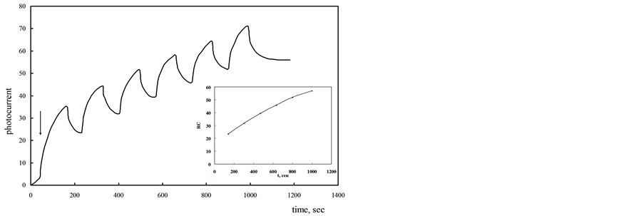
Figure 4. Photoresponse of the irradiated n-GaP crystal to a series of light pulses (λ = 0.5 mkm). The insert shows the set value RC vs. the illumination period after one of regular switching off the light.
light, high conductivity is registered for a long-time.
The insert in Figure 4 shows time dependence of RC. It is seen that RC increases with time and tends to saturation. It should be noted that at any point in time after turning off the light, RC is constant and has a certain value (except for a slow growth of dark current). That is, in the case of irradiated GaP a controlled selection of RC or photoelectric memory is possible. These results may be useful when creating certain geometric structures for the construction of long-time relaxing photoresists or memory systems.
4. Conclusions
As a result of electron irradiation, N-GaP crystals become highly photosensitive with a residual conductivity and long-time relaxation.
It was shown that the photoconductivity of irradiated GaP crystals takes place in a spectral range where additional absorption is observed, which agrees with a conclusion [2] about nature of additional absorption in irradiated GaP.
A quenching of RC in GaP crystals containing disordered regions is observed when illuminated by 300 K light with the threshold energy of 1eV (l = 1.24 mkm), which corresponds to the potential barrier height of clusters, and hence defines the Fermi level in it. It was found that at low temperatures, due to freezing of charge carriers at shallow donors in non damaged matrix of GaP, the photoionization from them prevailed over the quenching of RC.
It is revealed that the energy levels of radiation defects are distributed quasi-continuously in disordered regions, where conductivity is close to self-conductance. Here, the Fermi level is 1.0 eV below the bottom of conduction band.
It is shown that electron irradiation of n-GaP crystals can be used for a controlled selection of needed residual conductivity or photoelectric memory.
REFERENCES
- M. K. Sheinkman and A. Ja. Schick, Physics and Technique of Semiconductors, No. 10, 1976, pp. 209-233. (in Russian)
- E. Yu. Brailovskii, N. E. Grigoryan and G. N. Eritsyan, Physica Status Solidi (A), Vol. 62, 1980, pp. 649-655. http://dx.doi.org/10.1002/pssa.2210620237
- G. E. Zardas, et al., Solid State Communications, Vol. 105, 1998, pp. 77-79. http://dx.doi.org/10.1016/S0038-1098(97)10065-5
- V. S. Vavilov, et al., Uspekhi Phyizicheskikh Nauk, Vol. 169, 1999, pp. 209-212. (in Russian)
- G. Zardas, Ph. Yannakopoulos, C. Symeonides, O. Csabay and P. Euthymiou, Materials Science, Vol. 23, 2005, pp. 985-988.
- G. Zardas, Ph. Yannakopoulos, M. Ziska, C. Symeonides, P. Euthymiou and O. Csabay, Microelectronics Journal, Vol. 36, 2005, pp. 1-4.
- A. H. Kalma and J. C. Correlli, Physical Review, Vol. 173, 1968, pp. 734-745. http://dx.doi.org/10.1103/PhysRev.173.734
- R. F. Konopleva and V. N. Ostroumov, “The Interaction of High Energy Charged Particles with Germanium and Silicon,” Atomizdat, Moscow, 1975. (in Russian)
- M. K. Bachadyrchanov, S. B. Isamov, N. F. Zikrillaev and E. U. Arzikulov, Surface Engineering and Applied Electrochemistry, Vol. 49, 2013, pp. 308-311.
- S. M. Spitzer and I. C. North, Journal of Applied Physics, Vol. 44, 1973, pp. 214-219. http://dx.doi.org/10.1063/1.1661864
- E. Ju. Brailovskii, et al., Physics and Technique of Semiconductors, Vol. 9, 1975, pp. 769-771. (in Russian)
NOTES
*Corresponding author.