World Journal of Condensed Matter Physics
Vol.3 No.1(2013), Article ID:28311,4 pages DOI:10.4236/wjcmp.2013.31008
The Crystallographic and Optical Studies on Cobalt Doped CdS Nanoparticles
![]()
Advanced Materials Research Laboratory, Department of Physics, Dr. Babasaheb Ambedkar Marathwada University, Aurangabad, India.
Email: *drbndole.phy@gmail.com
Received June 9th, 2012; revised September 10th, 2012; accepted September 21st, 2012
Keywords: Nanocrystals; Chemical Synthesis; Grain Size; FTIR Spectra
ABSTRACT
The samples of Cd1−xCoxS with compositions x = 0.0 & 0.6 were prepared by Co-precipitation route at room temperature. XRD analysis confirms that the samples have cubic structure with no impurity phases. The lattice parameter, volume cell, X-ray density and grain size were calculated using XRD data. It is found that lattice parameter, volume of unit cell and X-ray density decrease with enhancing Co content. It is due to the smaller ionic radius of Co than the Cd. It is well noticed that the grain size increases with increasing Co content, it may be owing to the good synthesis technique. The functional groups and chemical interaction were determined by FTIR spectra. From FTIR spectra, it is investigated that absorption bands show the presence of resonance interaction between vibrational modes of oxide ions in the crystal. The energy band gap of Co doped CdS samples was calculated using UV-Vis analysis. It is observed that energy band gap decreases with increasing Co content owing to the sp-d exchange interaction between Co and CdS atoms.
1. Introduction
Recently, diluted magnetic semiconductors (DMS) have attracted considerable attention owing to their potential applications in spintronics. They can exploit both the spin and the charge of degree of freedom which promise new functionality of memories, detectors, and light emitting sources [1,2]. These materials have large number of applications in the fields of solar cell, microelectronics, catalysis, optical communications and light emitting diode [3,4]. On the other hand, Cadmium sulfide (CdS) is an important semiconductor compound of the II-VI group with excellent physical properties and band gap of 2.4 eV. Cadmium sulfide is an interesting material for optoelectronic device applications and has been extensively studied in light emitting diodes, photocatalysis, biological sensors, solar cells and photo degradation of water pollutants [5-10]. It is observed that Li & Eu doped CdS Nanomaterials are studied widely in the reported literature [11-17].
In this paper, we report the crystallographic and optical studies of of Co doped CdS nanoparticles. The Co doped CdS samples were characterized by X-ray diffracttion (XRD), Fourier transmission infrared (FT-IR) spectroscopy & UV-Vis spectra.
2. Experimental
The samples of Cd1−xCoxS nanoparticles with concentration x = 0.0 & 0.06 were prepared by Co-precipitation route. The chemicals cadmium acetate, thioacetamide, cobalt nitrate were dissolved in 50 ml of ethyl alcohol in separate beakers and stirred for 1 h with the help of magnetic stirrer. After 1 h the solution of cobalt nitrate was added drop wise in the solution of cadmium acetate and kept for 30 minutes. Then the solution of thioacetamide was added into the mixture of cadmium acetate and cobalt nitrate. This solution again stirred for 1 h, filtered using a filter paper and then washed with ethanol to remove impurity present in it. The residue was collected and dried at room temperature. After that each sample is ground for 15 min.
3. Results and Discussion
3.1. XRD Study
Figure 1 shows XRD patterns of samples are recorded at room temperature. XRD patterns of the samples reveal that they have cubic structure with no extra peaks of impurity phases. This suggests the material is in single phase form with homogeneous powder of finer particle size. The peak intensity goes on decreasing with increasing Co concentration.
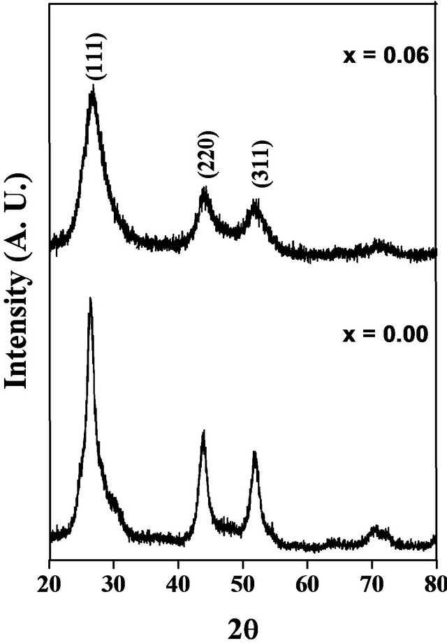
Figure 1. XRD patterns of Cd1−xCoxS system.
The structural data obtained from XRD patterns are tabulated in Table 1. From XRD data it is observed that the lattice parameter “a” decreases with increasing Co content. It is also observed that decrease in volume of unit cell with increasing Co concentration. This may be due to the ionic radius of Co ion (0.745 Å) which is smaller than that of Cd ion (0.97 Å). From lattice parameter calculations it is confirmed that Co ions go into the CdS lattice structure. The X-ray density was calculated using molecular weight and volume of unit cell of the samples following formula [18]. It is observed that volume of unit cell goes on decreasing with increasing Co concentration.
 (1)
(1)
where, n is the number of atoms per cell, M is the molecular weight of the sample, NA is Avogadro’s number (6.023 × 1026 molecules/kg-mole) and V is the unit cell volume.
The average grain size was calculated using DebyeScherrer’s formula [19].
 (2)
(2)
where λ is the wave length of the X-ray diffraction, θ is the diffraction angle and β- is full width at half maximum (FWHM) and obtained values are listed in Table 1. It is found that the grain size decreases with increasing Co concentration. It may be due to the enhancement in surface-to-volume ratio.
3.2. FTIR Study
The FTIR spectra for grown samples Cd1−xCoxS with composition (x = 0.00 & 0.06) were recorded at room temperature as shown in Figure 2" target="_self"> Figure 2.
The IR spectra at 3330.5005 cm−1, 1292.0384 cm−1 975.0978 cm−1 and some other associated peaks are shown in Figure 2. For x = 0.00, the peak appeared at 3330.5005 cm−1 indicates the presence of -OH stretching. This may be due to the atmospheric moisture. The peaks at 1666.7054 cm−1, 1397.0487 cm−1 are assigned to the vibrational mode of OH bending. The peak at 1292.0984 cm−1 shows the presence of symmetric stretching in the molecule. The strong absorption bond at 1107.7556 cm−1 is assigned to the symmetric stretching (C=O bond). The absorption peak at 2438.9155 cm−1 is assigned to the C-H group which suggests the presence of species in the surface of nanocrystals. The peak at 1292.038 cm−1 shows the asymmetric stretching. The peaks at 975.0978 cm−1 show the shoulders with asymmetric stretching and at 713 cm−1 shows additional symmetric stretching.
For x = 0.06, the peak at 3359.299 cm−1 corresponds to -OH stretching in water molecule. This peak indicates that the presence of bond corresponding to nitrate is clearly observed. The shoulders at 2473.9190 1667.8106, 1440.2882 cm−1 may due to the microstructure formation of the sample. The bond around at 1150.9952 cm−1 is due to the characteristic frequency at lower frequency. These modes indicate the presence of resonance interaction between vibration modes of CdS ions in the crystal. The peaks at 415.9231 cm−1 show the asymmetric bending.
Table 1. Lattice parameter, volume of unit cell, X-ray density and grain size of Cd1−xCoxS System with concentration (x = 0.00 & 0.06).
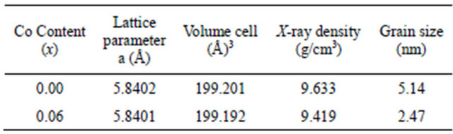
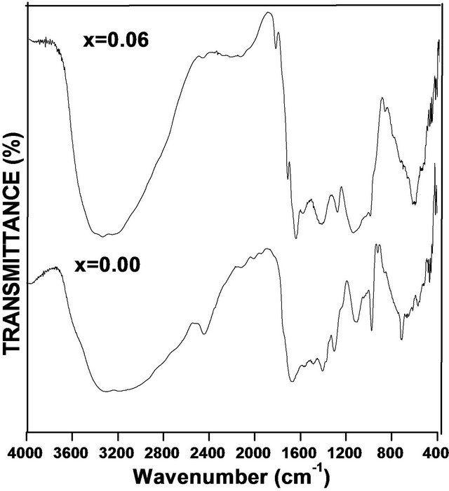
Figure 2. FTIR spectra of Cd1−xCoxS samples.
3.3. UV-Vis Study
The optical transition energies (energy band gap) of prepared samples are shown in Figure 3.
From Figure 3, it is observed that the optical band gap decreases from 2.32 eV to 2.24 eV with increasing Co concentration. The decrement of energy band gap is mainly due to sp-d exchange interaction between the band electrons and the localized d electrons of Co2+ ions doped for CdS ions [20]. The energy band gap measurement of our samples is performed at room temperature owing to this band gap is smaller than that of bulk CdS samples. Whereas Thambidurai et al. [21] published that the band gap of undoped and Co substituted CdS samples is greater than that of bulk CdS due to the above room temperature. It reflects good experimental results which were expected.
4. Conclusion
The samples of Cd1−xCoxS compound were synthesized successfully by Co-precipitation method. From XRD data, it is confirmed that all samples are in the cubic CdS structure. The volume of unit cell and X-ray density was calculated from XRD data. It is found that the volume of unit cell and X-ray density decrease as Co concentration increases. It indicates the incorporation of Co at Cd sites. It is due to the larger ionic radius of Cd ions as compared to the Co ions. The grain size of the crystalline has been computed by Debye Scherer’s equation. It is observed that the average crystallite size decreases with increasing Co content. Prominent IR peaks are analyzed & assigned by FTIR measurement. Absorption bands show the presence of resonance interaction between vibrational modes of oxide ions in the crystal. The reduction in energy band gap with increasing Co content, it may be due to sp-d exchange interaction between Co and CdS atoms.
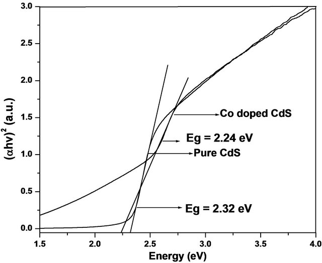
Figure 3. Energy band gap of Cd1−xCoxS samples.
5. Acknowledgements
Authors are grateful to Prof. S. S. Shah (Rtd), Department of Physics, Dr. B. A. M. University Aurangabad, for his valuable scientific discussion and also University Grants Commission, New Delhi, India for financial assistance through project No. (F-37-563/2009/SR).
REFERENCES
- S. A. Wolf, D. D. Awschalon, J. M. Daughton, S. Von Molnar, M. L. Roukes, A. Y. Chtchelkanova and D. M. Tregewr, “Spintronics: A Spin-Based Electronics Vision for the Future,” Science, Vol. 294, No. 5546, 2001, pp. 1488-1495. doi:10.1126/science.1065389
- H. Ohno, “Making Nonmagnetic Semiconductors Ferromagnetic,” Science, Vol. 281, No. 5369, 1998, pp. 951-956. doi:10.1126/science.281.5379.951
- M. Nirman and L. Brus, “Luminescence Photophysics in Semiconductor Nanocrystals,” Accounts of Chemical Research, Vol. 32, No. 5, 1999, pp. 407-414. doi:10.1021/ar9700320
- R. C. Ahoori, “Electrons in Artificial Atoms,” Nature, Vol. 379, No. 1, 1996, pp. 413-419. doi:10.1038/379413a0
- D. L. Klein, R. Roth, A. K. L. Lim and A. P. Alivisatos, “A Single-Electron Transistor Made from a Cadmium Selenide Nanocrystals,” Nature, Vol. 389, No. 6652, 1997, pp. 699-701. doi:10.1038/39535
- V. Ruxandra and S. Antohe, “The Effect of the Electron Irradiation on the Electrical Properties of Thin Polycrystalline CdS Layers,” Journal of Applied Physics, Vol. 84, No. 2, 1998, pp. 727-733. doi:10.1063/1.368129
- V. L. Kolvin, M. C. Schlamp and A. P. Alivisatos, “LightEmitting Diodes Made from Cadmium Selenide Nanocrystals and a Semiconducting Polymer,” Nature, Vol. 370, No. 6488, 1994, pp. 354-357. doi:10.1038/370354a0
- N. Romeo, A. Bosio and A. Romeo, “An Innovative Process Suitable Toproducehigh-Efficiency CdTe/CdS ThinFilm Modules,” Solar Energy Materials Solar Cells, Vol. 94, No. 1, 2010, pp. 2-7. doi:10.1016/j.solmat.2009.06.001
- A. P. Alivisatos, “Semiconductor Clusters, Nanocrystals, and Quantum Dots,” Science, Vol. 271, No. 5251, 1996, pp. 933-937. doi:10.1126/science.271.5251.933
- S. Bachir, K Azuma, J. Kossanyi and P. Valat, “Photoluminescence of Polycrystalline Zinc Oxide Co-Activated with Trivalent Rare Earth Ions and Lithium. Insertion of Rare-Earth Ions into Zinc Oxide,” Journal of Luminescence, Vol. 75, No. 1, 1997, pp. 35-49. doi:10.1016/S0022-2313(97)00093-8
- S. Tiwari, “Development of CdS Based Stable Thin Film Photo Electrochemical Solar Cells,” Solar Energy Materials & Solar Cells, Vol. 90, No. 11, 2006, pp. 1621-1628. doi:10.1016/j.solmat.2005.01.021
- C. B. Murray, D. J. Norris and M. G. Bawendi, “Synthesis and Characterization of Nearly Monodisperse CdE (E = Sulfur, Selenium, Tellurium) Semiconductor Nanocrystallites,” Journal of the American Chemical Society, Vol. 115, No. 19, 1993, pp. 8706-8715. doi:10.1021/ja00072a025
- X. Peng, J. Wickham and A. P. Alivisatos, “Kinetics of II-VI and III-V Colloidal Semiconductor Nanocrystal Growth: ‘Focusing’ of Size Distributions,” Journal of the American Chemical Society, Vol. 120, No. 21, 1998, pp. 5343-5344. doi:10.1021/ja9805425
- H. Zhang, X. Fu, S. Niu, G. Sun and Q. Xin, “Luminescence Properties of Li+ Doped Nanosized SnO2:Eu,” Journal of Luminescence, Vol. 115, No. 1-2, 2005, pp. 7-12. doi:10.1016/j.jlumin.2005.02.008
- Y. Qian, K. Hara, H. Munekata and H. Kukimoto, “BlueEmitting Ac-Electroluminescent Cells Based on ZnS:Tm, Li Powder Phosphors,” Japanese Journal of Applied Physics, Vol. 34, No. 3B, 1995, pp. L368-L370. doi:10.1143/JJAP.34.L368
- J. C. Ronfard-Haret and J. Kossanyi, “Electroand Photoluminescence of the Tm3+ Ion in Tm3+- and Li+-Doped ZnO Ceramics. Influence of the Sintering Temperature,” Chemical Physics, Vol. 241, No. 3, 1999, pp. 339-349. doi:10.1016/S0301-0104(98)00431-5
- V. D. Mote, V. R. Huse, K. M. Jadhav, B. N. Dole and S. S. Shah, “Synthesis and Structural Properties of Mn Doped ZnO Nanoparticles by Ceramic Route,” Bionano Frontiers, 2010, pp. 145-150.
- A. M. Abdeen, O. M. Hemeda, E. E. Assem and M. M. ElSehly, “Structural, Electrical and Transport Phenomena of Co Ferrite Substituted by Cd,” Journal of Magnetism and Magnetic Materials, Vol. 238, No. 1, 2002, pp. 75-83. doi:10.1016/S0304-8853(01)00465-6
- A. Patterson, “The Scherrer Formula for X-Ray Particle Size Determination,” Physical Review, Vol. 56, No. 10, 1939, pp. 978-982.
- P. Koidl, “Optical Absorption of Co2+ in ZnO,” Physical Review B, Vol. 15, No. 5, 1977, pp. 2493-2499. doi:10.1103/PhysRevB.15.2493
- M. Thambidurai, N. Muthukumarswami, D. Velauthapillai, S. Agilan and R. Balasundaraprabhu, “Structural, Optical and Electrical Properties Cobalt Doped CdS Quantum Dots,” Journal of Electronica Materials, Vol. 41, No. 4, 2012, pp. 665-672. doi:10.1007/s11664-012-1900-5
NOTES
*Corresponding author.