World Journal of Condensed Matter Physics
Vol.2 No.3(2012), Article ID:22159,5 pages DOI:10.4236/wjcmp.2012.23026
Increasing ZnO Growth Rate by Modifying Oxygen Plasma Conditions in Plasma-Assisted Molecular Beam Epitaxy
![]()
Department of Electrical Engineering, The City College of New York, New York, USA.
Email: *ashen@ccny.cuny.edu
Received January 27th, 2012; revised February 28th, 2012; accepted March 15th, 2012
Keywords: ZnO; MBE; Plasma-Assisted MBE; Growth Rate
ABSTRACT
The authors report that the growth rate of ZnO can be significantly increased by modifying the oxygen plasma conditions in plasma-assisted molecular beam epitaxy. Both the aperture diameter and the distance between the plasma source and the substrate affect the growth rate and the quality of the ZnO films. A short source to substrate distance is essential in achieving higher growth rate, which is explained by reduced chance of oxygen atom collisions to accommodate the short oxygen mean free path at high background pressure. At a shorter source to substrate distance, the growth rate is higher with a larger aperture diameter. The quality of the ZnO thin films grown under different conditions is assessed by x-ray diffraction and room-temperature photoluminescence measurements.
1. Introduction
ZnO is a wide bandgap semiconductor with a direct bandgap of 3.37 eV at room temperature. The unique properties of ZnO and related compounds and structures make them potential materials for novel photonic devices working in the ultraviolet and visible light region. More efficient light emitting devices may be realized due to the large exciton binding energy of ZnO (60 meV) [1,2]. ZnO is also a potential candidate for intersubband devices [3], especially for terahertz quantum cascade lasers working at room temperature [4], which is benefited from its large optical phonon energy (72 meV) [5]. Very recently, fractional quantum Hall effect has been reported in ZnO/ ZnMgO heterostructures with electron mobility exceeds 180.000 cm2/Vs [6]. Electrically pumped lasing from ZnO nanowires has also been reported [7].
ZnO thin films have been prepared by various growth techniques including radio frequency (RF) magnetron sputtering, pulsed-laser deposition (PLD), chemical-vapor deposition, and molecular-beam epitaxy (MBE). Among these, MBE has several advantages over the others such as the capability to grow high purity films under ultrahigh vacuum conditions and the precise control of the growth procedure by applying in situ diagnostic tools. Plasma-assisted MBE (PAMBE) is the main approach in MBE growth of ZnO, in which the atomic oxygen was either generated by a RF plasma source or by an electron cyclotron resonance plasma source. PAMBE has been proven to yield ZnO films with the highest material quality [8]. Critical parameters for PAMBE growth of ZnO are Zn flux, O2 flow, substrate temperature, and plasma power [8]. It has been reported that the growth rate of ZnO increases with the increase of plasma power [9,10]. For the growth with RF plasma sources, with a fixed total holes area (same conductance) of the aperture plate, the number of holes has also been shown to be correlated to the growth rate [10]. In this article, we report that the distance between the RF source and the substrate as well as the aperture diameter significantly affects the growth of ZnO thin films.
2. Experiment
The growth was performed in a modified DCA 350 MBE system. Elemental Zn and O2 gas, both with 6N purity, were used as source materials. Atomic oxygen was generated from an OAR CARS25AI atom/radical beam source, which is operated under a forward RF power of 350 W. Alumina aperture plates with two different diameters were used. Both aperture plates have 37 holes and the same hole distribution, as shown in the inset of Figure 1. The hole diameter for the small aperture is 0.5 mm and that for the large aperture is 1.5 mm. The optimum oxygen flow rates are 0.6 sccm and 4.0 sccm when the aperture plates with small and large holes are used, respectively. The RF plasma source cell was placed at two different positions which result in two different source to substratedistance (measured from the aperture plate) of 25.5 cm and 42 cm.
All samples were grown on 2” single-side polished epi-ready (0001) sapphire substrates. The substrates were mounted on indium-free molybdenum blocks and loaded into the growth chamber. Before the growth, the substrates were annealed at 720˚C for 30 minutes. The base pressure in the growth chamber is approximately 2.5 × 10⁻⁹ torr. During the growing, the background pressures were  torr and
  torr when 0.5 mm aperture and 1.5 mm aperture were used, respectively. All samples were grown under oxygen limit conditions at a substrates temperature of 600˚C for 4 hours. Typical beam equivalent pressures for Zn are 1.0 × 10⁻⁷ torr and 4.0 × 10⁻⁷ torr with the small and large aperture holes, respectively. No buffer layer was employed. The layer thicknesses were determined by Surface Profiler (Veeco De4kak 150) after wet etching with diluted HCl solution, The properties of the ZnO thin films were characterized by high resolution x-ray diffraction (Bruker D8 Advance x-ray diffractometer) and room-temperature photoluminescence (PL) measurements.
3. Results and Discussions
Samples A, B, and C are three typical samples grown under three different plasma source configurations. Samples A and B were grown with the aperture plate with 0.5 mm aperture diameter while sample C was grown with the aperture plate with 1.5 mm aperture diameter. Sample A was grown with a long source to substrate distance (42 cm) while samples B and C were grown with a short source to substrate distance (25.5 cm).
We started the experiments with a long source to substrate distance and with an alumina aperture plate with 0.5 mm aperture diameter. Under these growth conditions the growth rate is very low. As showed in Figure 1, for a typical sample grown under these conditions (Sample A) the growth rate is about 30 nm per hour. In order to achieve a higher growth rate, we replaced the aperture plate with a plate with a larger aperture diameter (1.5 mm). In principle, when the RF plasma source works under optimized conditions a fixed pressure within the discharge tube has to be maintained. Therefore larger apertures result in a larger oxygen flow. In fact, the optimum flow rate was increased from 0.6 sccm to 4.0 sccm when the aperture diameter was increased from 0.5 mm to 1.5 mm. However, with the increase of oxygen flow, instead of getting a higher growth rate we were unable to obtain any ZnO films. We explain the observation by the decrease of mean free path of oxygen atoms due to the increase of background pressure.
The mean free path is the average distance a moving particle could travel without collisions, as expressed by the following equation [11]
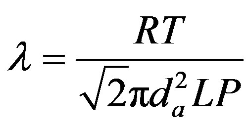 (1)
(1)
where λ is the mean free path, R the gas law constant (8.314510 joule·K–1·mole–1), L the Avogadro’s number (6.0221367 × 10²³ mole–1), T the temperature (300 K), da the Collisional Cross Section, and P the pressure. According to Equation (1), the mean free path of the active atomic oxygen is inversely proportional to the background pressure in the growing chamber. By replacing the alumina plate with small apertures with the one with large apertures the background pressure increased by an order of magnitude which results in the decrease of oxygen mean free path by an order of magnitude. Using da = 3.04 × 10⁻¹⁰ m and P = 2 × 10⁻⁴ torr, a mean free path is estimated to be 38 cm, which is very close to the source to substrate distance of 42 cm. Therefore at that source to substrate distance, most of the oxygen atoms generated by the RF source collide to form oxygen molecules, which cannot be used for ZnO growth.
To prove our assumptions, we reduce the distance between the RF source and substrate to 25.5 cm. Sample C is a typical sample grown under that short source to substrate distance (with large apertures). A growth rate of approximately 680 nm per hour was obtained for samples with a source to substrate distance of 25.5 cm and an alumina plate aperture diameter of 1.5 mm (Figure 1).
With the short source to substrate distance the growth rate is also greatly increased when the alumina plate with a small aperture diameter is used. Sample B is a typical
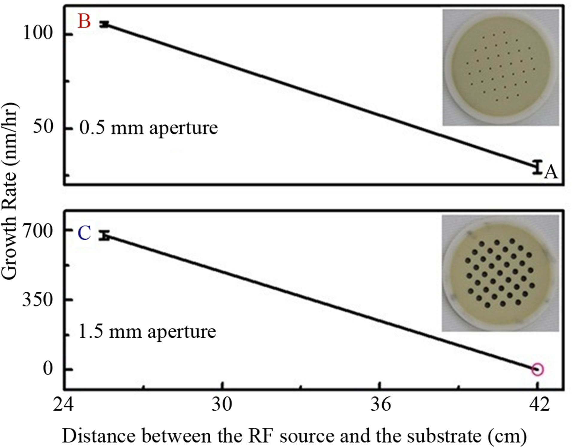
Figure 1. ZnO growth rate as a function of source to substrate distance for two different alumina plate aperture diameters.
sample grown under these conditions. The growth rate is approximate 105 nm per hour (Figure 1). The increase of growth rate with the decrease of source to substrate distance is attributed to the increase of atomic oxygen density at the substrate surface as schematically illustrated in Figure 2. If we neglect the aperture plate size, the ratio of atomic oxygen density is reversely proportional to the square of the ratio of the source to substrate distance. Therefore the decrease of the source to substrate distance from 42 cm to 25.5 cm increases the atomic oxygen density by 2.7 times, which is quite close to the actual increase of the growth rate by 3.5 times (105/30).
Figure 3 shows the XRD rocking curves obtained with (0002) reflection. The full width at half maximum (FWHM) for sample A, B, and C are 0.025˚, 0.015˚, and 0.063˚ respectively. The results show that generally for samples grown with large apertures and/or with too high a growth rate (like sample C) the structural quality of films is significantly degraded. Although the FWHM value of sample A is slightly larger than that of sample B, considering that sample B is nearly 4 times thicker than sample A, their structural quality may actually comparable. For all our samples, XRD pole figure measurements showed that there are no rotation domains in the films. Figure 4 is a typical ( ) XRD phi scan for one of our samples. The 6-fold symmetry indicates that the ZnO has hexagonal crystal structure. No secondary peaks are observed, which is evidence that there are no rotation domains in our films. Rotation domains have been widely reported in ZnO when the films are directly grown on c-plane sapphire by PAMBE [12-17].
Figure 5 shows the PL spectra for samples A, B, and C, which were measured at room temperature with a 266 nm solid state laser as the excitation source. All the samples showed a predominant emission peak at 3.30 eV. The FWHM values of the PL spectra for samples A, B, and C are 109 meV, 105 meV, and 126 meV, respectively, indicating the degrading of optical quality for the samples
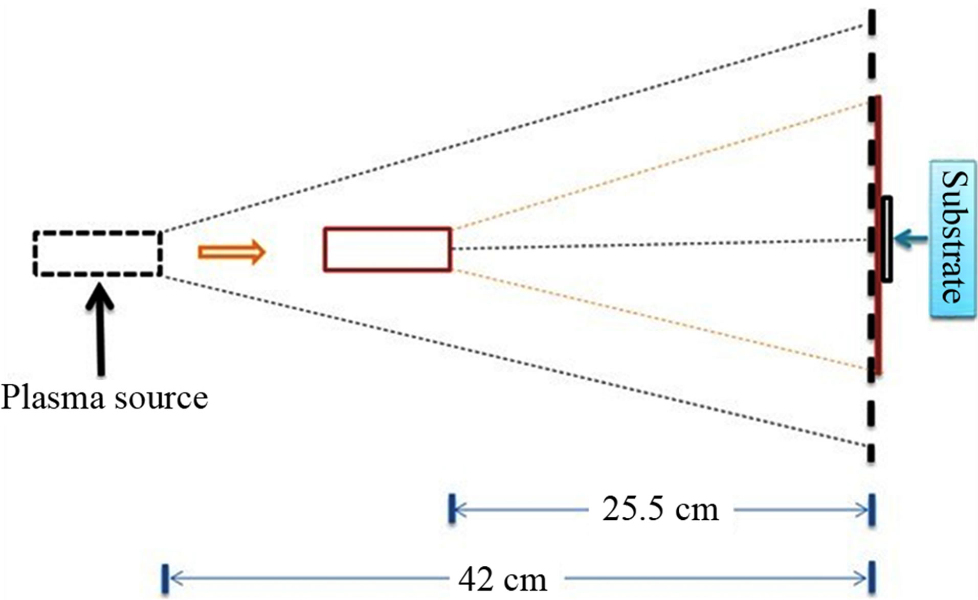
Figure 2. A schematic drawing showing the increase of oxygen atom density at the sample surface when the source to substrate distance is reduced.
grown with large apertures and/or with too high a growth rate. This result is consistent with the XRD rocking curve measurement results. The peak intensity of the PL spectra decreases with the increase of the growth rate (the inset of Figure 5), also suggest the degrading of optical quality with the increase of the growth rate.
4. Conclusion
We have studied the growth of ZnO thin films under different plasma configurations and found that the growth rate can be increased by reducing the distance between the RF source and the substrate. At a short source to substrate distance, the growth rate is higher with an alumina
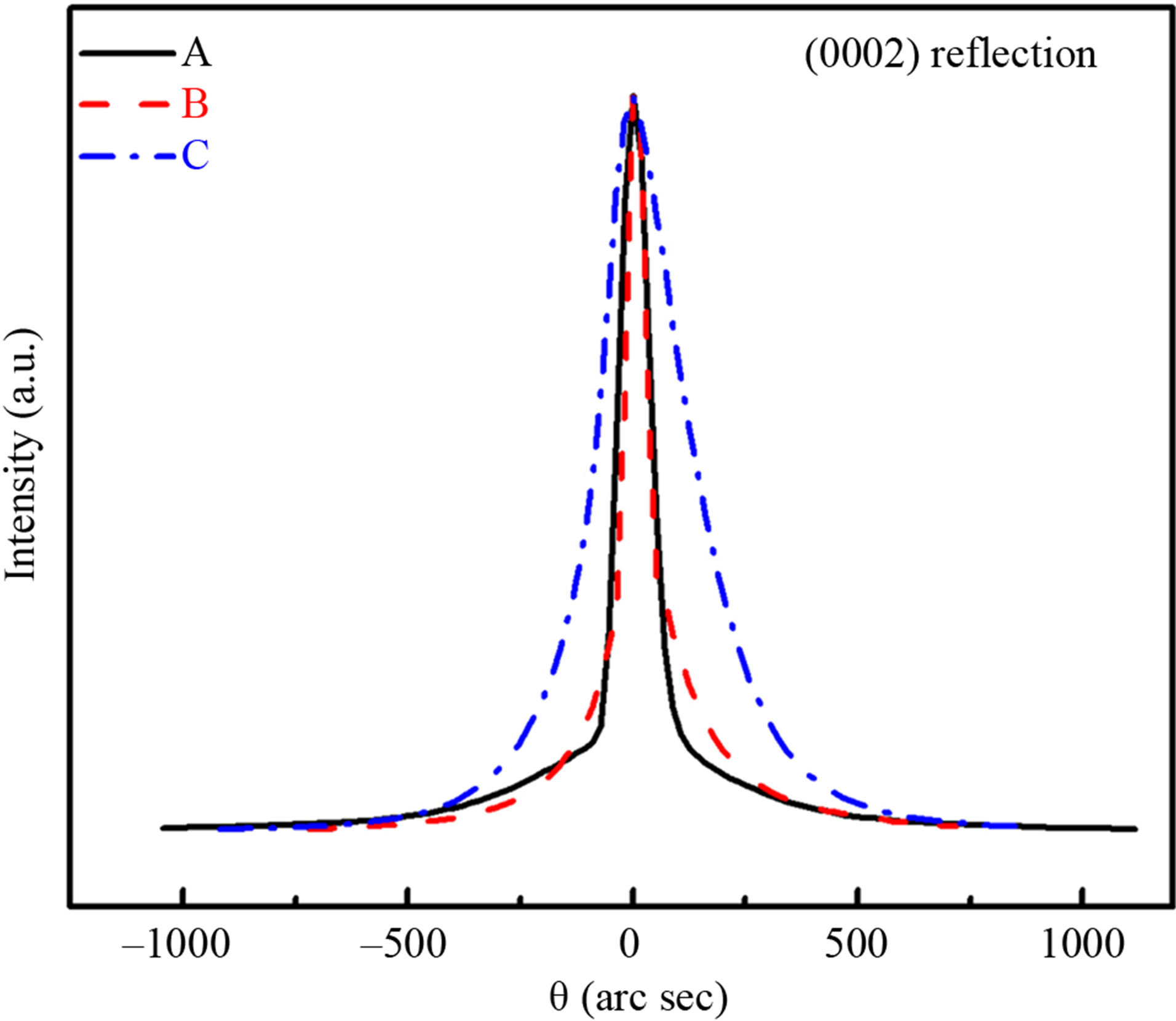
Figure 3. X-ray rocking curves obtained with (0002) reflection for a set of samples grown under difference plasma source configurations.
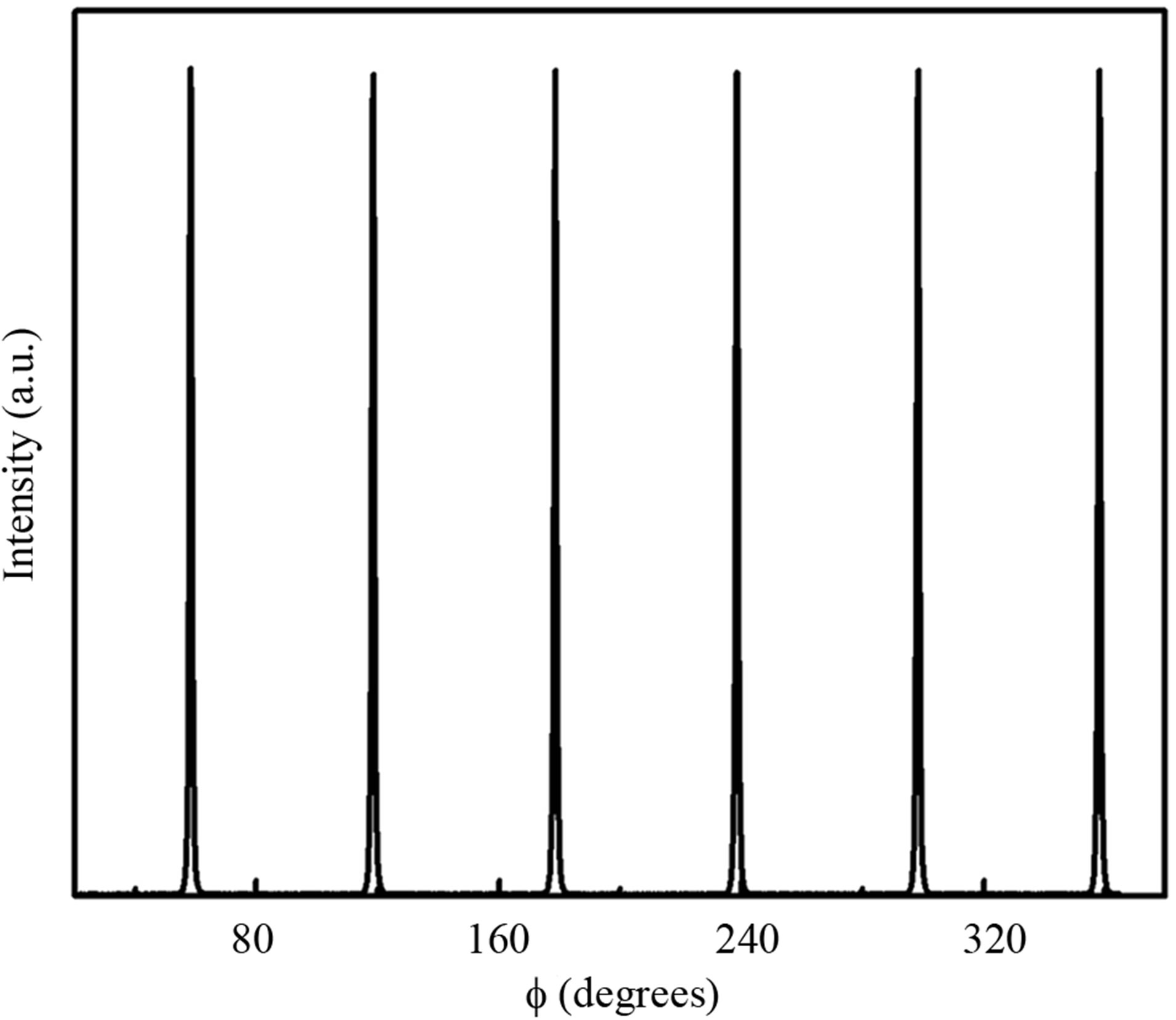
Figure 4. X-ray phi scan with ( ) reflection for a typical ZnO thin film grown on c-plane sapphire substrate.
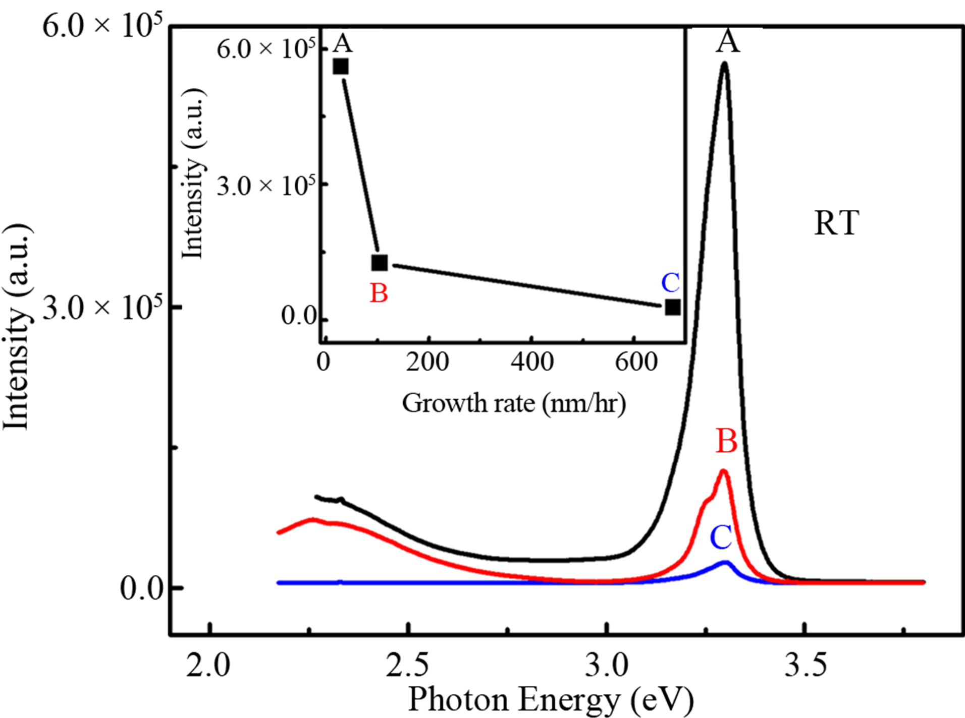
Figure 5. Room temperature PL spectra for a set of ZnO thin films grown under difference plasma source configurations.
plate with a larger aperture diameter (with the same hole distribution). The observation was explained by the decrease of oxygen mean free path with the increase of background pressure and the increase of atomic oxygen density with the decrease of source to substrate distance. We demonstrated that high crystalline quality ZnO thin films without rotation domains could be grown on c-plane sapphire substrates without applying any buffer layers. XRD and PL measurement results indicate that quality of the films is degraded for ZnO grown with a larger aperture diameter and/or too high a growth rate.
5. Acknowledgements
This work is supported in part by NSF grant # ECCS- 1028364, NSF grant # HRD-0833180, by Army Research Office grant # W911NF0810419 and by PS-CUNY Award.
REFERENCES
- D. G. Thomas, “The Exciton Spectrum of Zinc Oxide,” Journal of Physics and Chemistry of Solids, Vol. 15, No. 1-2, 1960, pp. 86-96. doi:10.1016/0022-3697(60)90104-9
- S. F. Chichibu, T. Sota, G. Cantwell, D. B. Eason and C. W. Litton, “Polarized Photoreflectance Spectra of Excitonic Polaritions in a ZnO Single Crystal,” Journal of Applied Physics, Vol. 93, No. 1, 2003, pp. 756-758. doi:10.1063/1.1527707
- M. Belmoubarik, K. Ohtani and H. Ohno, “Intersubband Transitions in ZnO Multiple Quantum Wells,” Applied Physics Letters, Vol. 92, No. 19, 2008, Article ID: 191906. doi:10.1063/1.2926673
- E. Bellotti, K. Driscoll, T. D. Moustakas and R. Paiella, “Monte Carlo Simulation of Terahertz Quantum Cascade Laser Structures Based on Wide-bandgap Semiconductors,” Journal of Applied Physics, Vol. 105, No. 11, 2009, Article ID: 113103. doi:10.1063/1.3137203
- T. C. Damen, S. P. S. Porto and B. Tell, “Raman Effect in Zinc Oxide,” Physical Review, Vol. 142, No. 2, 1966, pp. 570-574. doi:10.1103/PhysRev.142.570
- A. Tsukazaki, S. Akasaka, K. Nakahara, Y. Ohno, H. Ohno, D. Maryenko, A. Ohtomo and M. Kawasaki, “Observation of the Fractional Quantum Hall Effect in an Oxide,” Nature Materials, Vol. 9, No. 11, 2010, pp. 889- 893. doi:10.1038/nmat2874
- S. Chu, G. P. Wang, W. H. Zhou, Y. Q. Lin, L. Chernyak, J. Z. Zhao, J. Y. Kong, L. Li, J. J. Ren and J. L. Liu, “Electrically Pumped Waveguide Lasing from ZnO Nanowires,” Nature Nanotechnology, Vol. 6, No. 8, 2011, pp. 506-511. doi:10.1038/nnano.2011.97
- J. Chang, S.-K. Hong, K. Matsumoto, H. Tokunaga, A. Tachibana, S. W. Lee and M.-W. Cho, “Growth of ZnO and GaN Films,” In: T. Yao and S.-K. Hong, Eds., Oxide and Nitride Semiconductors, Springer, Berlin, 2009, pp. 67-129. doi:10.1007/978-3-540-88847-5_3
- Z. Yang, J. H. Lim, S. Chu, Z. Zuo and J. L. Liu, “Study of the Effect of Plasma Power on ZnO Thin Films Growth Using Electron Cyclotron Resonance Plasmaassisted Molecular-beam Epitaxy,” Applied Surface Science, Vol. 255, No. 5, 2008, pp. 3375-3380. doi:10.1016/j.apsusc.2008.09.068
- W. C. T. Lee, P. Miller, R. J. Reeves and S. M. Durbin, “Effects of Plasma Conditions on Properties of ZnO Films Grown by Plasma-Assisted Molecular Beam Epitaxy,” Journal of Vacuum Science & Technology B, Vol. 24, No. 3, 2006, pp. 1514-1518. doi:10.1116/1.2192540
- J. F. O’Hanlon, “A User’s Guide to Vacuum Technology,” Wiley, New York, 2003. doi:10.1002/0471467162
- P. Fons, K. Iwata, A. Yamada, K. Matsubara and S. Niki, “Uniaxial Locked Epitaxy of ZnO on the Face of Sapphire,” Applied Physics Letters, Vol. 77, No. 12, 2000, pp. 1801-1803. doi:10.1063/1.1311603
- X. L. Du, M. Murakami, H. Iwaki and A. Yoshikawa, “Complete Elimination of Multi-angle Rotation Domains in ZnO Epilayers Grown on (0001) Sapphire Substrate” Physica Status Solidi A, Vol. 192, No. 1, 2002, pp. 183- 188. doi:10.1002/1521-396X(200207)192:1<183::AID-PSSA183>3.0.CO;2-K
- M. J. Ying, X. L. Du, Z. X. Mei, Z. Q. Zeng, H. Zheng, Y. Wang, J. F. Jia, Z. Zhang and Q. K. Xue, “Effect of Sapphire Substrate Nitridation on the Elimination of Rotation Domains in ZnO Epitaxial Films,” Journal of Physics D: Applied Physics, Vol. 37, No. 21, 2004, pp. 3058-3062. doi:10.1088/0022-3727/37/21/017
- A. Yoshikawa, X. Q. Wang, Y. Tomita, O. H. Roh, H. Iwaki and T. Ishitani, “Rotation-Domains Suppression and Polarity Control of ZnO Epilayers Grown on Skillfully Treated c-Al2O3 Surfaces,” Physica Status Solidi B, Vol. 241, No. 3, 2004, pp. 620-623. doi:10.1002/pssb.200304236
- Z. L. Lu, W. Q. Zou, M. X. Xu and F. M. Zhang, “Struc-Tural and Electrical Properties of Single Crystalline and Bi-Crystalline ZnO Thin Films Grown by Molecular Beam Epitaxy,” Chinese Physics B, Vol. 19, No. 7, 2010, Article ID: 076101. doi:10.1088/1674-1056/19/7/076101
- T. Trautnitz, R. Sorgenfrei and M. Fiederle, “Elimination of Rotation Domains in ZnO Thin Films on c-Plane Al2O3 Substrates,” Journal of Crystal Growth, Vol. 312, No. 4, 2010, pp. 624-627. doi:10.1016/j.jcrysgro.2009.12.011
NOTES
*Corresponding author.