Open Journal of Physical Chemistry
Vol. 2 No. 3 (2012) , Article ID: 22125 , 4 pages DOI:10.4236/ojpc.2012.23025
KCl Single Crystals Growth with Mn, Ag and in Impurities by Czochralski Method and Study of Impurities Influence on Their Properties
1Physics Department, Bu-Ali Sina University, Hamedan, Iran
2Physics Department, Imam Hossein University, Tehran, Iran
Email: *fsamavat@yahoo.com, ehajiali@yahoo.com, somayeh.solgi@yahoo.com, p_taravati@yahoo.com
Received February 14, 2012; revised April 1, 2012; accepted May 3, 2012
Keywords: Single crystal; KCl; Czochralski; X-ray diffraction; Chemical etching; Vickers micro hardnes
ABSTRACT
In this research KCl, KCl:Mn, KCl:Ag and KCl:In single crystals have been grown by Czochralski method. X-ray diffraction confirms KCl single crystal formation. In this work also influence of mentioned impurities on the optical property of KCl single crystal has been studied by chemical etching. Then the hardness of these crystals have been measured by Vickers micro hardness. The result indicate the positive effect of the impurity on optical and mechanical properties.
1. Introduction
After one century from the start of the crystal growth, many efforts of researches have been devoted to it. This is because of vast application of crystal in the construction of physical devices such as detectors, solid-state lasers, scintillators and other optical pieces. In general three kinds of crystals are always considered. Scintillator crystal, crystals with the use of laser and optical crystals.
This is the three types of crystals have been grown with technology of crystal growth from melting by crystal growth Czochralski and Brigman methods [1]. Crystal with mentioned applications which often are alkali halides, after semiconductors such as silicon; arsenid gallium; and etc, have the most of world annual production of crystal [2]. One from the most important application of optical crystals is production of optical window of lasers. For construction of this component is needed to material with uniform structure, wide gap band and good mechanical strength[1]. Single crystal of KCl, with wide gap band (~8 eV), structure of uniform and simple cubic, is used in production of optical windows.
In a survey, windows made from KCl comparison with the windows from ZnS, Gar and etc have been had so much better efficiently in Co2 laser windows [3]. Although this crystal has undesirable properties such as attractive moisture, poor thermal and mechanical properties. But with adding of heavy impurities it can replace for the crystals used in lasers, scintillators and telecommunications equipment optical fiber with low-cost and efficient [4]. In this study the crystal growth of KCl with heavy impurities and effect of increasing of impurity on the properties of these crystals are investigated.
2. Crystal Growth
Crystal growth by Czochralski method is based on slow pull of seed from melt free surface. This action is associated with the exact regulation of the temperature of the furnace during slow pull. In this method, with changing of pulling speed of seed and also rate of increasing and the decreasing of the furnace temperature, can get a crystal with needed size and shape.
In this paper, we are describing the growth of the single crystal of KCl by Czochralski method with the impurities of Mn, In and Ag in approximate size diameter 50 mm, length 40 mm (single crystal with impurity In is more slender). For growth this crystals was used from Alumina (Al2O3) crucible. This crucible has good physical properties such as high mechanical strength and resistance to environmental factors such as moisturing. In addition, its melting temperature is higher than experiment material.
For growth of the single crystal of KCl with 0.02 impurity of Mn, 100 gr KCl powder with 0.03 gr MnCl2 powder have been mixed in crucible. The crucible is placed within furnace of the growth system. This furnace has two elements, one for heating of the wall and the other for floor. The furnace has turn on by temperature control digital system (that temperature control is responsible for both elements) and is heated with rate of 20˚C/min from room temperature to 930˚C. For the confidence from complete melting and homogenization of the materials, the temperature increase to 930˚C from the room temperature melting temperature of KCl powder is 771˚C.
After complete melting of the material and getting a thermodynamic equilibrium, changing rate of furnace temperature is decreased from 3˚C/min to 0.3˚C/min is changed. Furnace temperature fluctuations are decreased and growth process is controlled easier. A single crystal of KCl with length of 30 mm is used as seed. The seed is contacted with melting free surface vertically by pulling the seed holder slowly and with rotation speed 30 rpm [5].
After peeling, again seed has been placed in temperature a little lower than the melting temperature and with pulling rate of 5 mm/h, so the initial nucleus is formed on seed.
After than, the neck part of crystal is being growth with speed of more pulling. The crystal neck is a narrow part with length of 10 mm to 15 mm. Finally, the crystal shoulder is forming with pulling speed of 6 mm/h and gradually reduce the temperature of the furnace. For forming of crystal body, the temperature is kept constant and pulling is done more quickly. Figure 1 shows that the crystal of KCl:Mn in growing.
After ending of growth, annealing process is performed for 24 h in the temperature of 600˚C. The single crystals KCl with impurities of In and Ag, also have been growth via mentioned method. Figure 2 shows the single crystals KCl:Ag and KCl:In after annealing.
These crystals were analyzed then cut into small pieces for studying of structure and their quality.
3. Analysis of Grown Crystals
3.1. X-Ray Diffraction (XRD)
Radiation of X-beam to a sample is obtained information
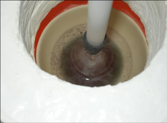
Figure 1. The single crystal KCl:Mn in growing.
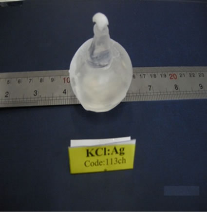
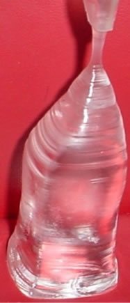
Figure 2. The single crystals KCl:Ag and KCl:In after exit of the furnace.
such as structure, material gender, elements amount in the sample. XRD of single crystal of KCl:In is obtained by apparatus of Ital Structure, that is set on 40 kV and 30 mA. Sample is scanned in range of 2θ =10˚ to 2θ = 20˚ with step of 2θ = 0.01˚.
Figure 3 shows X-ray diffraction spectrum of single crystal of KCl:In.
Survey of XRD spectra of single crystals of KCl:Mn and KCl:Ag performed by Philips apparatus with diffract meter 1800 pw, which is set on 40 kV and 30 mA. Samples were scanned in range of 2θ = 10˚ to 2θ = 90˚ with step of 2θ = 0.02˚. Figures 4 and 5 show XRD spectra of these crystals.
3.2. Chemical Etching
Chemical etching is a method for determination crystal quality. In this method can be estimated crystal dislocation. Alkali halides are prepared often via growth from melting. Thus, they are in thermal stress. The thermal gradient import stress into the crystal and cause of combining of present dislocations in seed that continued to boundary of solid-melting [6].
If the crystal is placed in the condition that atoms is separated of surface, the atoms of around of dislocation will separate with higher speed from the crystal and holes are been formed in their site. That to they are been called the Etchpit. The Etchpit is criterion from further dislocation.
The used corrosion solution for crystals of KCl is solution of acetic acid with 4 gr from powder of FeCl3 [7].
Fresh-cut pieces of crystals are contacted with the corrosive solution and this time is noted. Then crystal pieces are dried and their surfaces are observed with transmission microscope of model JNOEC J6-20 and with magnification of 400. The mentioned corrosion solution will not get clear Etchpit for single crystals of KCl:Mn and KCl:Ag, thus for they are used from corrosion solution of pure acetic acid.
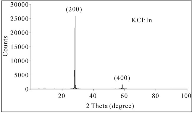
Figure 3. XRD spectrum of KCl:In.
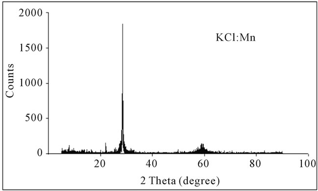
Figure 4. XRD spectrum of KCl:Mn.

Figure 5. XRD spectrum of KCl:Ag.
Table 1 and Figure 6 show the results of this experiment and picture of Etchpit of single crystal of KCl:Ag.
3.3. Hardness
Hardness is materials resistance to infiltration or to become punctured by more difficult material [8].
Hardness is divided to macroscopic and microscopic hardness. Vickers micro hardness is a kind from microscopic hardness which is used for measurement of hardness of thin metals and fragile. In this way, applied load to the sample is equal or less than 1000 gr [9].
In this experiment, the pieces are cut in same size from crystals. These pieces have been tested with mass of 10

Table 1. The results chemical etching.
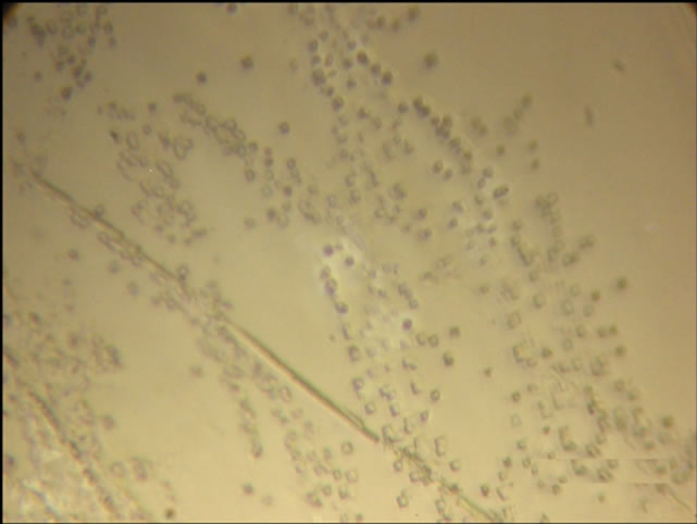
Figure 6. The picture of Etchpit from chemical etching in the surface of the crystal of KCl:Ag.
gr at time of 15 s. The results of samples have been reported in Table 2.
the above results show increasing of impurities in single crystal of KCl have positive effects in increasing of hardness of the single crystal. This result is clearer when impurity atom is heavier and bigger. The data of chemical etching Table 1 confirm these results. Figure 7 shows matching of results of two experiments. During growth process and particularly at the end of growth impurity atoms put in dislocation seat.
The existence of such great atoms is prevented from dislocation motion, because of large energy require for movement of the atoms.
4. Discussion and Conclusion
In XRD spectra of samples are observed high peak with low width (2θ = 0.06˚) thus samples are single crystal. In all samples, the main peak is in 2θ = 28.3˚. This peak is corresponding to plane (200) than single crystal is grown in main direction of (200). Weaker peak is occurred in 2θ = 58.6˚. This peak is corresponding to diffraction from plane of (400) that is harmonic of plane (200). As chemical etching results show density of Etchpit of crystals that is in order 105 cm−2. The density of crystals , that are used in optical purposes , is in order 104 to 106 cm−2 [10]. Thus the grown crystals have good optical quality
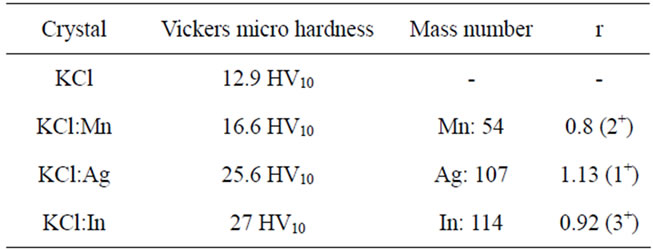
Table 2. Results of Vickers micro hardness.
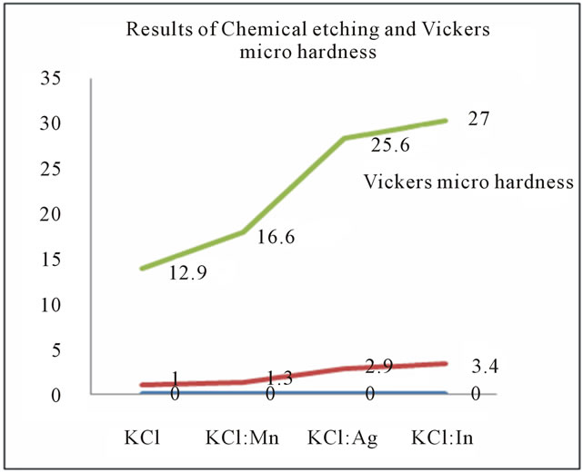
Figure 7. Comparison of results chemical etching and vickers micro hardness.
and are suitable for optical applications. As adding of impurity to pure crystal of KCl was increased hardness of this crystal, that is a positive step in improving of their mechanical properties.
REFERENCES
- S. G. Singh, M. Tyagi, D. G. Desai, A. K. Singh, B. Tiwari, S. SeN, A. K. Chauhan and S. C. Gadkari, “Development of Technologically Important Crystals and Devices,” BARC Newsletter, No. 318, 2011, pp. 16-27.
- H. G. Scheel, “Estimated Shares of World Crystal Production,” Journal of Crystal Growth, Vol. 211, No. 1-4, 2000, pp. 1-12. doi:10.1016/S0022-0248(99)00780-0
- G. Atanassov, D. Popov and P.-F. Gu, “Antireflection Coatings on KC1 Single-Crystal Windows with Low Optical Loss,” Thin Solid Films, Vol. 261, 1995, pp. 256-262.
- S. Polosan, T. Tsuboi, E. Apostol and V. Topa, “Electrolytic Reduction of Tl+ Ions in KCl Crystals,” Optical Materials, Vol. 30, No. 1, 2007, pp. 95-97. doi:10.1016/j.optmat.2006.11.006
- M. Tyagi, S. G. Singh, A. K. Singh and S. C. Gadkari, “Understanding Colorations in PbMoO4 Crystals through Stoichiometric Variations and Annealing Studies,” Physica Status Solid A, Vol. 207, No. 8, 2010, pp. 1802- 1807. doi:10.1002/pssa.200925625
- F. Rosenberger and G. H. Westphal, “Low-Stress Physical VAPOR Growth,” Journal of Crystal Growth, Vol. 43, No. 2, 1978, pp. 148-152. doi:10.1016/0022-0248(78)90162-8
- K. Sangwal, “Eching of Crystals,” North Holland, 1987.
- www.leco.com/resources/met_tips/met_tip9.pdf
- D. B. Sirdeshmukh, L. Sirdeshmukh and K. G. Subhadra, “Micro and Macro Properties of Solids,” Springer-Verlag Berlin Hidelberg, 2006.
- N. B. Singh, T. A. Gould and R. H. Hopkins, “Etching Studies on Crystals of Thalium Arsenic Selenide,” Journal of Crystal Growth, Vol. 78, No. 1, 1996, pp. 43-50.
NOTES
*Corresponding author.