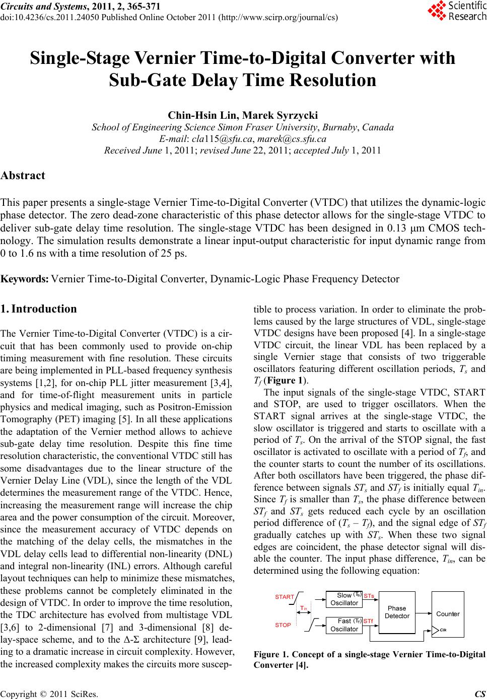
C.-H. LIN ET AL.371
(a) (b)
(c)
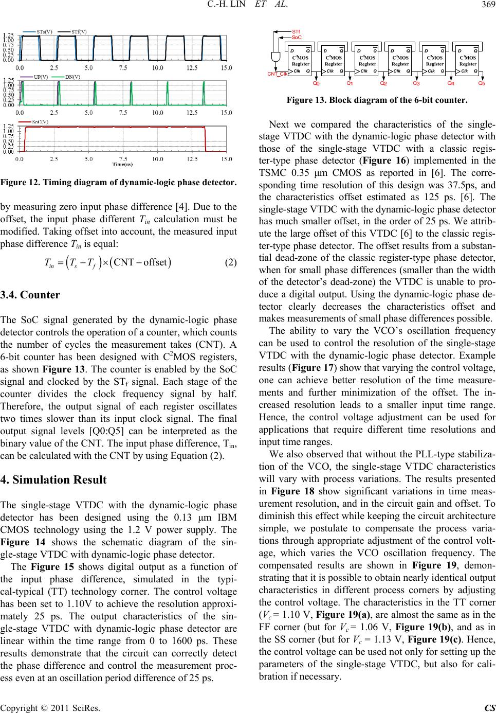
Figure 19. Digital output characteristics of the single-stage
VTDC with the dynamic-logic phase detector in the differ-
ent process corners compensated using different values of
the control voltage (a) TT corner Vc = 1.10 V; (b) FF corner,
Vc = 1.06V; (c) SS corner, Vc = 1.13 V.
5. Conclusions
This paper presents a single-stage Vernier Time-to-
Digital Converter with sub-gate delay time resolution.
By utilizing the dynamic-logic phase detector that elimi-
nates the dead-zone problem, the single-stage Vernier
Time-to-Digital Converter in this work has demonstrated
a linear digital output characteristic with a 25 ps time
resolution. The presented simulation results have con-
firmed the very important role of the phase detector qual-
ity for the performance of single-stage Vernier Time-
to-Digital Converters with sub-gate delay resolutions.
6. References
[1] R. B. Staszewski, S. Vernulapalli, P. Vallur, et al., “1.3V
20ps Time-to-Digital Converter for Frequency Synthesis
in 90-nm CMOS,” IEEE Transactions on Circuits and
Systems II, Vol. 53, No. 3, 2006, pp. 220-224.
doi:10.1109/TCSII.2005.858754
[2] R. B. Staszewski, C.-M. Hung, K. Maggio, et al., “All-
Digital Phase-Domain TX Frequency Synthesizer for
Bluetooth Radios in 0.13m CMOS,” IEEE International
Solid-State Circuit Conference (ISSCC), Vol. 1, 15-19
Feburary 2004, pp. 272-527.
doi:10.1109/ISSCC.2004.1332699
[3] C.-C. Chung and W.-J. Chu, “An All-Digital On-Chip
Jitter Measurement Circuit in 65 nm CMOS Technol-
ogy,” International Symposium on VLSI Design, Automa-
tion and Test, Hsinchu, 25-28 April 2011, pp. 1-4.
[4] A. H. Chan and G. W. Roberts, “A Jitter Characterization
System Using a Component-Invariant Vernier Delay
Line,” IEEE Transactions on Very Large Scale Integra-
tion (VLSI) Systems, Vol. 12, No. 1, 2004, pp. 79-95.
[5] B. K. Swann, B. J. Blalock, L. G. Clonts, et al., “A
100-ps Time-Resolution CMOS Time-to-Digital Con-
verter for Positron Emission Tomography Imaging Ap-
plications,” IEEE Journal of Solid-State Circuits, Vol. 39,
No. 11, 2004, pp. 1830-1845.
[6] P. Chen, C.-C. Chen, J.-C. Zheng and Y.-S. Shen, “A
PVT Insensitive Vernier-Based Time-to-Digital Con-
verter with Extended Input Range and High Accuracy,”
IEEE Transactions on Nuclear Science, Vol. 54, No. 2,
2007, pp. 294-302. doi:10.1109/TNS.2007.892944
[7] A. Liscidini, L. Vercesi and R. Castello, “Time to Digital
Converter Based on a 2-Dimensions Vernier Architec-
ture,” 2009 IEEE Custom Integrated Circuits Conference,
San Jose, 13-16 September 2009, pp. 45-48,
[8] J. J. Yu and F. F. Dai, “A 3-Dimensional Vernier Ring
Time-to-Digital Converter in 0.13m CMOS”, IEEE
Custom Integrated Circuit Conference (CICC), San Jose,
19-22 September 2010, pp. 1-4.
[9] Y. Cao, P. Leroux, W. De Cock and M. Steyaert, “A 1.7
mW 11b 1-1-1-MASH Δ-Σ Time-to-Digital Conver-
ter,” 2011 IEEE International Solid State Circuits Con-
ference, San Francisco, 20-24 February 2011, pp. 480-
482. doi:10.1109/ISSCC.2011.5746406
[10] T. A. Jackson and A. Albicki, “Analysis of Metastable
Operation in D Latches,” IEEE Transactions on Circuits
and Systems, Vol. 36, No. 11, 1989, pp. 1392-1404.
doi:10.1109/31.41296
[11] Z. Cheng and M. Syrzycki, “Modifications of a Dynamic-
Logic Phase Frequency Detector for Extended Detection
Range,” 2010 53rd IEEE International Midwest Sympo-
sium on Circuits and Systems, Seattle, 1-4 August 2010,
pp. 105-108. doi:10.1109/MWSCAS.2010.5548572
Copyright © 2011 SciRes. CS