International Journal of Communications, Network and System Sciences
Vol.10 No.08(2017), Article ID:78399,9 pages
10.4236/ijcns.2017.108B024
Research on Carrier Synchronization of QPSK Based on Simulink
Zhaoxu Zhang, Zhigang Li, Zheng Dou
Information and Communication Engineering College, Harbin Engineering University, Harbin, China


Received: June 17, 2017; Accepted: August 11, 2017; Published: August 14, 2017
ABSTRACT
As an important part of the communication system, synchronization technology is a communication system to run the correct protection, has been a hot topic in communication systems research. Four-phase phase shift keying (QPSK) circuit structure is relatively simple, and has a good band utilization, in the modern communication has a wide range of applications. Corresponding research on carrier synchronization for QPSK coherent demodulation is carried out. By comparing several carrier recovery loops, The quaternary loose tail loop is selected as carrier recovery loop. First of all, the core part of the digital phase-locked loop analysis and implementation, and finally through the tool Simulink to complete the realization of the system.
Keywords:
Carrier Synchronization, Quaternary Loose Tail Loop, Simulink, Digital Communication

1. Introduction
With the rapid development of modern communication and network technology, wireless communication technology development in the direction of digital, broadband-oriented. Modern communication systems require far communication distance, large communication capacity, good transmission quality and strong confidentiality. Synchronization technology has always been a hot research problem in communication systems.
QPSK technology is widely used in digital microwave communication systems, broadband access digital satellite communications systems, mobile communications and cable television systems. QPSK modulation is the best choice for digital satellite transmission for a number of reasons satellite power transmission efficiency, anti-interference and comprehensive consideration of the size of the antenna. QPSK demodulation generally uses coherent demodulation of the way, so there are high requirements on the performance of carrier synchronization [1]. Carrier synchronization is also known as carrier recovery, that is, through the receiving device to generate a carrier with the received signal synchronization in phase with the local oscillation, the receiver to do coherent demodulation [2].
Synchronization is also a kind of information, according to the acquisition and transmission of synchronous information, can be divided into external synchronization and self-synchronization method. By the sender to send a special synchronization information (often referred to as the pilot), the receiver to extract the pilot as a synchronization signal method, known as the external synchronization method, the sender does not send a special synchronization information, the receiver managed to extract the synchronization information from the received method, known as the self-synchronization method. The self-synchronization method is a more desirable synchronization method than the external synchronization method, because all the power and bandwidth can be assigned to the signal transmission [3].
Since QPSK modulation is to suppress the modulation of the carrier, there is no carrier component in the modulated signal, and the carrier needs to be recovered from the received signal to achieve coherent demodulation. To recover the carrier from the received signal, the signal must be processed non-linearly to produce the corresponding carrier component, and then filter out with a narrowband filter or phase-locked loop.
2. QPSK Modulation and Demodulation Algorithm
QPSK is the use of four different carrier phase to represent the digital information, each carrier phase by two bits. There are four combinations of two bits, namely 00, 01, 10 and 11. The carrier phase relationship between them and are arranged in accordance with the laws of the Gray code [4], which is expressed in two ways constellation diagram is shown in Figure 1.
The QPSK signal can be represented by Equation (1):
 (1)
(1)
where  is the carrier angle frequency, which
  is the carrier phase value of the kth symbol,
  is the duration of a transmission symbol, and
  is the waveform function of the transmitted symbol.
  takes one of the four carrier phase, the formula 1 can be obtained:
 (2)
(2)
Take ,
,  , values which are discrete values, and the related carrier phase, and an orthogonal vector corresponding to the same phase in the constellation diagram. It can be seen from Equation (2) that the waveform of QPSK modulation can be regarded as the sum of the signals of binary amplitude modulation for two orthogonal carriers. QPSK modulation through Simulink is
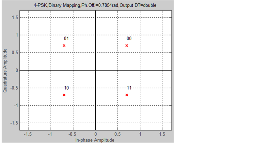
Figure 1. QPSK signal constellation.
shown in Figure 2.
Through the PN sequence generator to generate a set of 0 and 1 binary number, and then through the polarity conversion module into bipolar symbols, through the serial and parallel conversion module data into in-phase branch and orthogonal branch, they are multiplied by the carrier, and the two are added to obtain the QPSK modulation signal. The coherent demodulation of the QPSK signal enables two orthogonal carrier signals to be implemented. The quadrature branch and the in-phase branch are respectively set up two correlators (or matched filters) and then subjected to level decision and parallel conversion to restore the original information.

Figure 2. QPSK modulation model.
3. Carrier Synchronization Method and Algorithm
There are many ways to recover coherent carriers from suppressed signals of suppressed carriers. Commonly used methods are:
1) Quadrilateral loop: We will receive the QPSK signal for the fourth operation, and then use the frequency selection circuit to select the  component, and then divided by four to obtain the frequency of
  coherent carrier. This method brings some difficulty to the engineering implementation, and the quality of the coherent carrier is not high, which affects the quality of the communication.
2) Costas loop: Costas loop is also known as in-phase orthogonal loop. Its advantage lies in the extraction of coherent carrier at the same time to complete the I, Q two-way demodulation, and performance is also better. The Costas loop requires that the group delay and impulse response must be consistent in each low-pass channel, otherwise there will be some problem in the carrier recovery. Therefore, its drawback is that in addition to the actual adjustment loop more difficult, the loop itself has a limited range of capture, and sometimes cannot meet the actual needs of the project, and the reliability of the equipment is poor [5].
3) Inverse modulation loop: Compared with Costas loop, the inverse modulation loop avoids the two baseband multipliers, and the output signal of the VCO is compared with the external carrier signal by the loop phase detector to obtain the error voltage to adjust the oscillation of the VCO. In order to minimize the residual modulation of the output of the inverse modulator, it is necessary to adjust the delay between the distribution amplifier and the multiplier so that the resulting delay is equal to the delay generated by the demodulator section. This is the reverse modulation loop demodulation QPSK signal is the key, but also the most difficult to grasp the actual.
Based on the above three kinds of carrier recovery loops, it can be seen that different carrier recovery rings are seeking a reasonable compromise in loop performance (including capture range, capture accuracy, capture time) and engineering difficulty. And the quaternary loose tail loop is the compromise under the principle of a best carrier recovery program.
4) Quaternary loose tail loop: In the high-capacity digital communication system, the four-phase loose tail ring can guarantee high-quality carrier. The baseband processing circuit of the simulated Costas loop is replaced by a digital circuit, which greatly improves the performance and reliability of the loop. The quaternary loose tail loop circuit is simple and easy to realize integration. Baseband processing part of the easy to use digital implementation, and even the entire carrier recovery ring can be used to achieve all the digital circuit, the circuit will be greatly simplified.
3.1. The Principle and Simulation of Digital Phase-Locked Loop
In the above mentioned several carrier extraction methods, the core devices contain digital phase-locked loop structure. So we introduce the structure of the digital phase-locked loop, then use the tool Simulink to build a digital phase- locked loop and simulation [6].
A phase-locked loop is a circuit that synchronizes the output signal with the input signal by frequency and phase. In the synchronous (locked state), the output signal and the input signal frequency is equal, the phase difference is 0, or remain constant, that is, the output signal locked to the input signal phase. Digital phase locked loop consists of three basic parts: digital phase detector (DPD), digital loop filter (DLF) and digital voltage controlled oscillator (DCO).
The digital phase detector is a device for comparing the phase, and its effect is to compare the phase difference between the input signal and the DCO output signal and convert the phase difference into a voltage signal output. The digital phase detector appears in the Z-domain model as a zero-order module with gain of .
.
In the output signal of the phase detector, the DC component and the superposed AC component are included. We do not expect to see the AC component, which causes the oscillator output frequency to be unstable, so the filter is added to the filter to filter it, called the loop filter. Loop filter can be seen as a linear low-pass filter, it has two main functions, first, filter out the high-frequency components of the error signal; second, for the phase-locked loop to provide a short-term memory, if the system is unlocked due to transient noise, ensuring that the phase-locked loop quickly recaptures the signal. The transfer function of the phase-locked loop is [7]:
 (3)
(3)
where  and
and  are the charge and discharge time constants in the analog circuit and
  is the sampling time of the ADC, make:
 ,
, (4)
(4)
The digital voltage-controlled oscillator (DCO) can be viewed as a voltage- to-frequency device with its oscillation frequency controlled linearly by the input control voltage. The output of the DCO is fed back to the phase detector, so the output voltage of the phase detector output is not its instantaneous frequency, but its instantaneous phase. The DCO is an ideal integrator in the loop, and the transfer function is:
 (5)
(5)
Through the above digital phase-locked loop of the working principle of the introduction, through the tools Simulink simulation of the schematic diagram shown in Figure 3.
In Figure 3, the input signal is sine wave, the use of sin and cos trigonometric function module to simulate the stored sine value, that is, lookup table, respectively, multiplied by the multiplier and input signal multiplication. After the two-way after the output signal to the loop filter, where the simulation using the digital filter structure and exactly the same as described above, all the way for the equivalent integral structure, all the way for the zero-order amplification, these two parameters are calculated from the above formula of the phase-locked loop filter. Add the sampling time to each module. Finally, the input signal is compared with the output signal, as shown in Figure 4. Figure 4 in the digital phase-
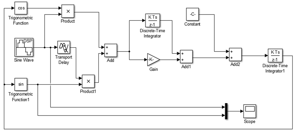
Figure 3. Digital phase-locked loop structure.

Figure 4. Digital phase-locked loop output signal and input signal.
locked loop output signal and the input signal is basically the same, indicating that the phase-locked loop can be a stable carrier, so the structure of the phase- locked loop is correct.
3.2. The Principle and Simulation of the Quaternary Loose Tail Loop
After the above analysis, the QPSK carrier tracking using the quaternary loose tail loop, the structure diagram shown in Figure 5.
When the system is in the locked state, assuming that the received QPSK signal is:
 (6)
(6)
The VCO output carrier is:
 (7)
(7)
The signal through the low-pass filter is:
 (8)
(8)
Equation (8) , after the adder and subtractor after the signal is:
 (9)
(9)
After the judge:

Figure 5. The quaternary loose tail loop structure.
 (10)
(10)
Finally:
 (11)
(11)
It can be seen from the formula 11, after the quaternary loose tail loop processing , there is no digital modulation signal, only contains the VCO and the input signal carrier phase difference
 . Therefore, the tracking of the QPSK signal of the quaternary loose tail loop is equivalent to a tracking of the unmodulated carrier with the ordinary phase-locked loop with
  phase discrimination. The principle of Simulink through the quaternary loose tail loop is shown in Figure 6. The carrier of the signal input and the carrier output through the four-phase loose tail ring are shown in Figure 7.

Figure 6. The structure of the quaternary loose tail loop based on Simulink.

Figure 7. The input carrier and carrier that is recovered by the quaternary loose tail loop.
4. Conclusion
The quaternary loose tail loop occupies less resources, good carrier recovery performance, while the use of pine tail ring baseband processing can also constitute 8PSK demodulation ring. The baseband processing of the loose tail loop can completely eliminate the modulation information in the modulated signal, so the demodulation ring formed by it will not introduce modulation noise and pattern noise at the phase lock. The quaternary loose tail loop is a QPSK baseband digital carrier recovery ring with simple engineering and good carrier recovery performance. It has been applied in many communication systems. The debugging results show that the designed system can be stable and reliable.
Acknowledgements
This paper is funded by the International Exchange Program of Harbin Engineering University for Innovation oriented Talents Cultivation, International Science & Technology Cooperation Program of China (2014DFR10240), National Natural Science Foundation of China (612111070), China Postdoctoral Science Foundation (2013T60346), Harbin Science and Technology Research Projects (P083313026), Natural Science Foundation of Heilongjiang Province (P083014025).
Cite this paper
Zhang, Z.X., Li, Z.G. and Dou, Z. (2017) Research on Carrier Synchronization of QPSK Based on Simulink. Int. J. Communications, Network and System Sciences, 10, 227-235. https://doi.org/10.4236/ijcns.2017.108B024
References
- 1. Huang, Z. (2005) Research on the Quaternary Loose Tail Loop and the Realization of FPGA. Master Thesis, Harbin Institute of Technology, Heilongjiang.
- 2. Xing, T., Dou, Z., Jin, Z. and Lin, Y. (2015) Improvement of PSK Signal Carrier Frequency Estimation Based on Hilbert-Huang Transform. Applied Science and Technology, No. 4, 37-42.
- 3. Zhu, W.P., Ahmad, M.O. and Swamy, M.N.S. (2003) Joint Carrier and Frame Synchronization for MPSK Demodulation. Proceedings of the 2003 International Symposium on Circuits and Systems (ICAS’03), 2, 25-28.
- 4. Fan, C.X. and Cao, L.N. (2011) Communication Theory. Six Edition, National Defence Industry Press, Beijing, 242-247.
- 5. Shoari, A., Kamalei, M. and Radmand, A. (2005) Implementation of Costas Loop Using CORDIC Algorithm for Software Radio Applications. IEE Proceedings- Commu-nications, 152, 113-118. https://doi.org/10.1049/ip-com:20040649
- 6. Deng, T., Jiang, C.J. and Lai, Z.S. (2006) An Improved First-Order Digital Phase-Locked Loop. Journal of East China Normal University (Natural Science Edition), No. 1, 132-135.
- 7. Li, S.G. and Yang, Z.J. (2005) An Improved All-Digital Phase-Locked Loop Design. Microcomputer Journal, 21, 42-44.