International Journal of Communications, Network and System Sciences
Vol.10 No.08(2017), Article ID:78320,6 pages
10.4236/ijcns.2017.108B001
High-Performance Structure of Guard Ring in Avalanche Diode for Single Photon Detection
Wei Wang, Yu Zhang, Zhenqi Wei
College of Electronic Information, Hangzhou Dianzi University, Hangzhou, China


Received: February 23, 2017; Accepted: August 11, 2017; Published: August 14, 2017
ABSTRACT
Avalanche photon diode and avalanche diode array, working in Geiger mode, have single photon detection capability. The structure of guard ring is the key factor to avoid the premature edge breakdown of the avalanche diode and increase the maximum bias voltage. A new structure of the guard ring is proposed in this letter, in which the floating guard ring is put outside the p-well guard ring. Simulation results indicate that the maximum bias voltage of the proposed guard ring is higher than that of the state-of-the-art methods.
Keywords:
Avalanche Photon Diode, Guard Ring, Premature Edge Breakdown, Maximum Bias Voltage, Single Photon Detection

1. Introduction
From the mid-1990s onwards, the use of dedicated CMOS-compatible processes fostered significant advances in building multichannel photon-counting modules, thus making SPAD devices become a robust and competitive technology to detect single photon like confocal microscopy, biological essays, particle detection, quantum key distribution, DNA microarray, LIDAR and adaptive optics in astrophysics [1] [2] [3]. The premature edge breakdown of the avalanche photon diode (APD) is an important factor that affects the single photon counting of the avalanche diode [4]. Guard ring is an effective method to prevent premature breakdown of avalanche diode [3]. At present, there are three kinds of guard rings in avalanche diode to prevent edge breakdown prematurely. Firstly, literature [4] [5] [6] designed diffused guard ring, which was to avoid the premature edge breakdown by creating a guard ring around the central active area of APD. Secondly, the floating guard ring was proposed in literature [7], making use of sub-pressure principle, which added some bias voltage to the edge of the floating guard ring, so the electric field in the edge region was less than that of the center of the active area. Finally, Leitner and Hendersonin literature [8] and [9] ameliorated the performance of virtual guard ring. All these above efforts are beneficial to prevent from the premature edge breakdown of the avalanche diode. However, these guard rings are not able to withstand the higher reverse bias voltage. The central active area and the edge of the above guard rings are easier to be broken down under high reverse bias voltage, which will influence the detection performance of APD. As a result, it is necessary to improve the structure of guard ring to make it can withstand high reverse bias voltage.
In order to keep away from premature edge breakdown and increase the maximum bias voltage of the avalanche diode, a new structure of guard ring in avalanche diode is proposed in this letter. In this new structure, p-guard ring is put outside the p-well guard ring, which not only reduce the electric field intensity of the edge of guard ring but also makes it possible to withstand higher reverse bias voltage.
2. The Proposed Structure of Guard Ring
Figure 1 is the proposed guard ring structure in the p+/n-well APD. As shown
 (a)
(a)
 (b)
(b)
Figure 1. The proposed guard ring structure in p+/n-well APD. (a) Schematic cross section of the proposed guard ring. (b) The simulation graph of APD with the proposed guard ring.
in Figure 1(a), the APD structure includes the deep n-well, the p-substrate and the p+ active area. The p-well diffused guard ring is put around the p+ active area and the floating guard ring (p-region) is put outside of the p-well. D (4 um) is the distance between the center of p-well and that of p-region. Figure 1(b) is the simulation graph of the proposed guard ring.
3. Simulation Results and Comparisons with Other Structures
In order to verify the performance of the proposed guard ring structure, virtual guard ring, diffused guard ring and floating guard ring are utilized to compare with it. All these guard rings are implemented in identical p+/n-well APD structure which is shown in Figure 1(a). In this section, all these structures are simulated by Silvaco Atlas 5.20.2.R software. Simulation conditions are set as Table 1 and the rest of parameters have been elaborated in Figure 1(a).
Figure 2 depicts the electric field intensities of the edges of different guard rings in identical APD structure under the same bias voltage (30 V).
It can be seen from Figure 2 that the color of the edge area of the proposed guard ring is shallow than that of other guard rings, which means the electric field intensity of the edge of proposed guard ring is lower than that of other guard rings under the same bias voltage. In other word, the proposed guard ring can withstand the higher reverse bias voltage than other guard rings. The maximum bias voltages of different guard rings in Figure 2 are shown in Figure 3.
From Figure 3, it can be obtained that the maximum bias voltage of the proposed guard ring is larger than that of other guard rings. That is to say, the proposed guard ring can avoid the premature edge breakdown better than other guard rings.
4. Conclusion
In this letter, a novel structure of guard ring in avalanche diode, putting the floating guard ring outside the p-well guard ring, is proposed. Compared with other guard rings, the proposed one is able to get the lower electric field intensity of the edge under the same bias voltage and the larger maximum bias voltage.

Table 1. Main parameters setting of APD structure.
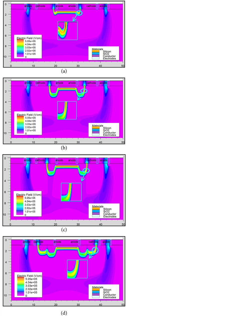
Figure 2. Electric field intensities of the edges of different guard rings in the same APD under the same bias voltage. (a) With virtual guard ring. (b) With diffused guard ring. (c) With floating guard ring. (d) With the proposed guard ring.

Figure 3. The maximum bias voltages of different guard rings. a: with virtual guard ring. b: with diffused guard ring. c: with floating guard ring. d: with the proposed guard ring.
The proposed guard ring supplies the possible solution to enhance the performance of the avalanche photon diode for single photon detection.
Acknowledgements
This work was supported by the National Natural Science Foundation of China under Grant No. 61372156 and No. 61306100 and by the Natural Science Foundation of Zhejiang Province under Grant No. LZ13F04001.
Cite this paper
Wang, W., Zhang, Y. and Wei, Z.Q. (2017) High-Performance Structure of Guard Ring in Avalanche Diode for Single Photon Detection. Int. J. Communications, Network and System Sciences, 10, 1-6. https://doi.org/10.4236/ijcns.2017.108B001
References
- 1. Deng, S., Gordon, D. and Morrison, A.P. (2016) A Geiger-Mode APD Photon Counting System with Adjustable Dead-Time and Interchangeable Detector. IEEE Photonics Technology Letters, 28, 99-102. https://doi.org/10.1109/LPT.2015.2487342
- 2. Bronzi, D., Villa, F., Tisa, S., Tosi, A., Zappa, F., Durini, D., Weyers, S. and Brockherde, W. (2014) 100,000 Frames/s 64 × 32 Single-Photon Detector Array for 2-D Imaging and 3-D Ranging. IEEE Journal of Selected Topics in Quantum Electronics, 20, 1-10. https://doi.org/10.1109/JSTQE.2014.2341562
- 3. Faramarzpour, N., Deen, M.J., Shirani, S. and Fang, Q.Y. (2008) Fully Integrated Single Photon Avalanche Diode Detector in Standard CMOS 0.18 m Technology. IEEE Transactions on Electron Devices, 55, 760-767. https://doi.org/10.1109/TED.2007.914839
- 4. Richardson, J.A., Webster, E.A.G., Grant, L.A. and Henderson, R.K. (2011) Scaleable Single-Photon Avalanche Diode Structures in Nanometer CMOS Technology. IEEE Transactions on Electron Devices, 58, 2028-2035. https://doi.org/10.1109/TED.2011.2141138
- 5. Niclass, C., Gersbach, M., Henderson, R., Grant, L. and Charbon, E. (2007) A Single Photon Avalanche Diode Implemented in 130-nm CMOS Technology. IEEE Journal of Selected Topics in Quantum Electronics, 13, 863-869. https://doi.org/10.1109/JSTQE.2007.903854
- 6. Kamrani, E., Lesage, F. and Sawan, M. (2014) Low-Noise, High-Gain Transimpedance Amplifier Integrated with SiAPD for Low-Intensity Near-Infrared Light Detection. IEEE Sensors Journal, 14, 258-269. https://doi.org/10.1109/JSEN.2013.2282624
- 7. Janekovic, I., Knezevic, T., Suligoj, T. and Grubisic, D. (2015) Optimization of Floating Guard Ring Parameters in Separate-Absorption-and-Multiplication Silicon Avalanche Pho-todiode Structure. The Proceedings of IEEE 38th International Convention on Information and Communication Technology, Electronics and Microelectronics, Hrvatska, Opatija, 25-29 May 2015, 37-41. https://doi.org/10.1109/mipro.2015.7160234
- 8. Leitner, T., Feiningstein, A., Turchetta, R., Coath, R., Chick, S., Vi-sokolov, G., Savuskan, V., Javitt M., Gal, L., Brouk, I., Bra-Lev, S. and Nemirovsky, Y. (2013) Measurements and Simulations of Low Dark Count Rate Single Photon Avalanche Diode Device in a Low Voltage 180-nm CMOS Image Sensor Technology. IEEE Transactions on Electron Devices, 60, 1982-1988. https://doi.org/10.1109/TED.2013.2259172
- 9. Henderson, R.K., Webster, E.A.G. and Grant, L.A. (2013) A Du-al-Junction Single-Photon Avalanche Diode in 130-nm CMOS Technology. IEEE Electron Device Letters, 34, 429-431. https://doi.org/10.1109/LED.2012.2236816