Y. ZHENG ET AL.107
for approximating the exact wave equation for mono-
chromatic waves and solving the resulting equation nu-
merically. For the monochromatic type of waves, such as
,, exp
yzi t
, in a three-dimensional waveguide,
the beam propagation method satisfies the scalar equa-
tion as follows [6,7]:
222 2
2
2222 ,, 0nxyz
xyzc
(1)
where is the propagation direction of waves,
z
is
the angular frequency, is the refractive index
of the incident medium, 0 is in-
troduced for the spatially-dependent wave number, and
is the wave number in free space. If
,,nxyz
,,kxy
exp n
,,z knxyz
0
k
,,
,,
yz uxyzikz
, then is the con-
stant number to be chosen to make , where
is slowly varying.
n
k
,,uxyz z
22
dudz can then be neglected with
respect to ddku z. With this assumption and after a
slight rearrangement, the above equation is reduced to
the following:
22
22
22
2n
n
uiu u
kku
zkxy
(2)
The three propagation media in the coupling interface
between the planar optical waveguide chip and optical
fibers are the core of the optical fiber, adhesive, and core
of the planar optical waveguide chip. To facilitate calcu-
lation, only the electric field E is considered. The mag-
netic field H can be calculated in the same way as the
electric field E. The propagation field may be discon-
tinuous in the coupling interface. The boundary can be
given by:
12
12
EnEn
Dn Dn
(3)
where is the normal direction of input light, 1 and
2 are the electric field of the first and second media,
respectively, and 1 and 2 are the electric flux den-
sity of the first and the second media, respectively.
nE
ED D
3. Results and Discussion
The light coupling between a planar optical waveguide
chip and an optical fiber can be calculated by the overlap
integral of the optical field distributions in a reference
plane. As the goal of the present study is to understand
the properties of the coupling interface for planar optical
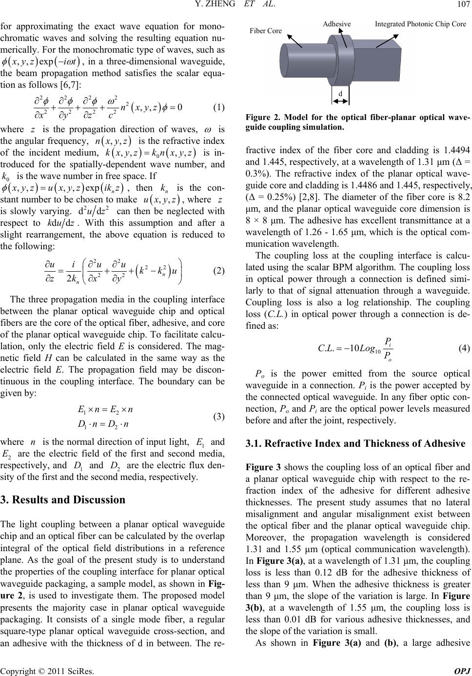
waveguide packaging, a sample model, as shown in Fig-
ure 2, is used to investigate them. The proposed model
presents the majority case in planar optical waveguide
packaging. It consists of a single mode fiber, a regular
square-type planar optical waveguide cross-section, and
an adhesive with the thickness of d in between. The re-
Fiber Core AdhesiveIntegrated Photonic Chip Core
d
Figure 2. Model for the optical fiber-planar optical wave-
guide coupling simulation.
fractive index of the fiber core and cladding is 1.4494
and 1.445, respectively, at a wavelength of 1.31 μm (Δ =
0.3%). The refractive index of the planar optical wave-
guide core and cladding is 1.4486 and 1.445, respectively,
(Δ = 0.25%) [2,8]. The diameter of the fiber core is 8.2
μm, and the planar optical waveguide core dimension is
8 × 8 μm. The adhesive has excellent transmittance at a
wavelength of 1.26 - 1.65 μm, which is the optical com-
munication wavelength.
The coupling loss at the coupling interface is calcu-
lated using the scalar BPM algorithm. The coupling loss
in optical power through a connection is defined simi-
larly to that of signal attenuation through a waveguide.
Coupling loss is also a log relationship. The coupling
loss (C.L.) in optical power through a connection is de-
fined as:
10
.. 10i
o
P
CLLog P
(4)
Po is the power emitted from the source optical
waveguide in a connection. Pi is the power accepted by
the connected optical waveguide. In any fiber optic con-
nection, Po and Pi are the optical power levels measured
before and after the joint, respectively.
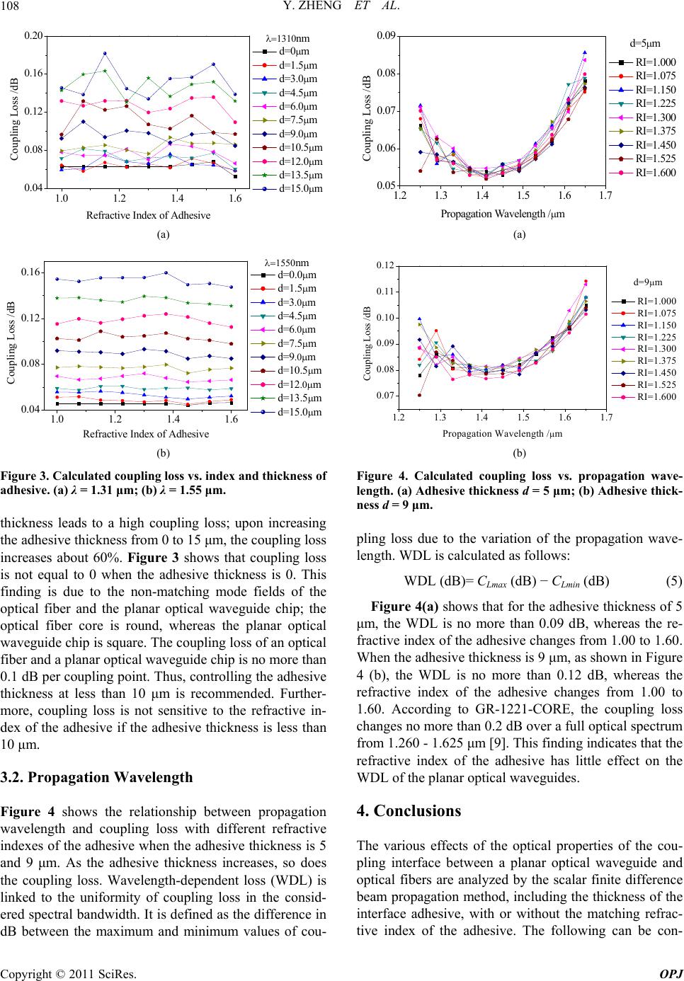
3.1. Refractive Index and Thickness of Adhesive
Figure 3 shows the coupling loss of an optical fiber and
a planar optical waveguide chip with respect to the re-
fraction index of the adhesive for different adhesive
thicknesses. The present study assumes that no lateral
misalignment and angular misalignment exist between
the optical fiber and the planar optical waveguide chip.
Moreover, the propagation wavelength is considered
1.31 and 1.55 μm (optical communication wavelength).
In Figure 3(a), at a wavelength of 1.31 μm, the coupling
loss is less than 0.12 dB for the adhesive thickness of
less than 9 μm. When the adhesive thickness is greater
than 9 μm, the slope of the variation is large. In Figure
3(b), at a wavelength of 1.55 μm, the coupling loss is
less than 0.01 dB for various adhesive thicknesses, and
the slope of the variation is small.
As shown in Figure 3(a) and (b), a large adhesive
Copyright © 2011 SciRes. OPJ