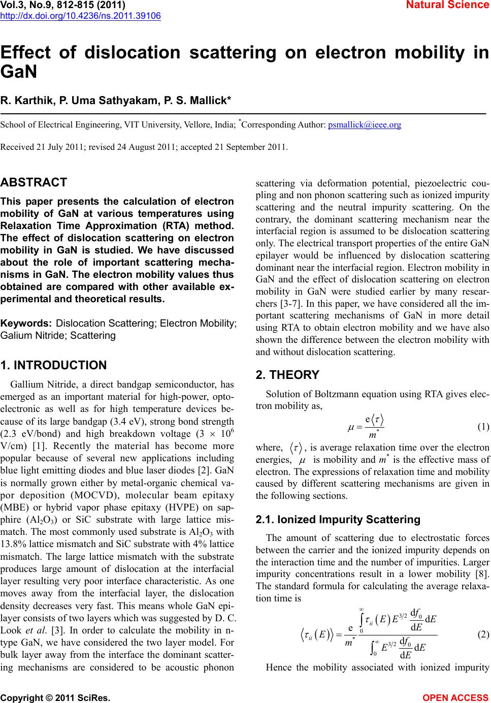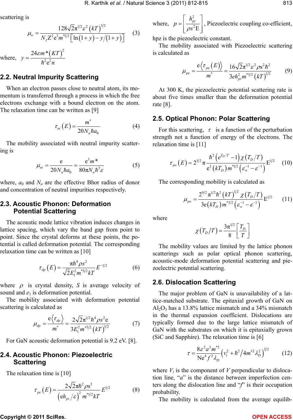
R. Karthik et al. / Natural Science 3 (2011) 812-815
Copyright © 2011 SciRes. OPEN ACCESS
815
mismatch and the consequence of these studies can help
them to obtain an accurate theoretical model.
REFERENCES
[1] Jain, S.C., Willander, M., Narayan, J. and Van Over-
straeten, R. (2000) III-nitride: Growth, characterization
and properties. Journal of Applied Physics, 87, 965.
doi:10.1063/1.371971
[2] Nakamura, S., Pearton, S.J. and Fasal, G. (2000) The blue
LASER diodes. Springer, Berlin.
[3] Look, D.C. and Sizelove, J.R. (1999) Dislocation Scat-
tering in GaN. Physical Review Letter, 82, 1237.
doi:10.1103/PhysRevLett.82.1237
[4] Dutikrushna, P., Sarkar, C.K., Mukhopadhyay, D. and
Mallick, P.S. (2005) Hot electron microwave incremental
conductivity of GaN. Journal of Optics, 34, 172-175.
[5] Hosein, E. (2009) The effect of hydrostati pressure on
material parameters and electrical transport properties in
bulk GaN. Physics Letters A, 373, 1773-1776.
doi:10.1016/j.physleta.2009.03.013
[6] Ng, H.M., Doppalapudi, D., Moustakas, T.D., Weimann,
N.G. and Eastman, L.F. (1998) The role of dislocation
scattering in n type GaN films. Applied Physical Letters,
73, 821. doi:10.1063/1.122012
[7] Weimann, N.G., Eastman, L.F., Doppalapudi, D., Ng,
H.M. and Moustakas, T.D. (1998) Scattering of electrons
at threading dislocations in GaN. Journal of Applied Physics,
83, 3656. doi:10.1063/1.366585
[8] Dhar, S. and Ghosh, S. (1999) Low field electron mobil-
ity in GaN. Journal of Applied Physics, 86, 2668.
doi:10.1063/1.371108
[9] Erginsoy, C. (1950) Neutral impurity scattering in semi-
conductors. Physical Review, 79, 1013.
doi:10.1103/PhysRev.79.1013
[10] Nag, B.R. (1980), Electron transport in compound semi-
conductors. Springer-Verlag, Berlin.
[11] Look, D.C. (1989) Electrical characterization of GaAs
materials and devices. Willey, New York.
[12] Lin, M.E., Sverdiov, B.N., Strite, S., Morkoe, H. and
Drakin, A.E. (1993) Refractive indices of Wurtzite and
Zincblende GaN. Electronics Letters, 29, 1759.
doi:10.1049/el:19931172
[13] Wang, Y.J., Kaplan, R., Ng, H.K., Doverspike, K., Gaskil,
D.K., Ikedo, T., Amano, H. and Akasaki, I. (1996) Mag-
neto-optical studies of GaN and GaN/AlxGa1-xN: Donor
zeeman spectroscopy and two dimensional electron gas
cyclotron resonance. Journal of Applied Physics, 79,
8007. doi:10.1063/1.362351
[14] Morkoc, H. (1999) Nitride Semiconductors and devices,
Springer-Verlag, Heidelberg/Berlin/New York.
doi:10.1007/978-3-642-58562-3
[15] Schroeder, D.K. (1990), Semiconductor material and
device characterization. Wiley, New York.
[16] Bykhovski, A.D., Kaminski, V.V., Shur, M.S., Chen, Q.C.
and Khan, M.A. (1996) Piezoelectric effect in wurtzite n
type GaN. Applied Physical Letters, 68, 818.
doi:10.1063/1.116543
[17] Shan, W., Schmidt, S., Yang, X.H., Song, J.J. and Golden-
berg, B. (1996) Optical properties of wurtzite GaN grown
by low-pressure metalorganic chemical-vapor deposition.
Journal of Applied Physics, 79, 3691.
doi:10.1063/1.361200
[18] Perlin, P., Staszewska, E.L. and Suchanek, B. (1996)
Determination of the effective mass of GaN from infrared
reflectivity and Hall effect. Applied Physical Letters, 68,
1114. doi:10.1063/1.115730
[19] Djeffal, F., Arar, D., Lakhdar, N., Bendib, T., Dibi, Z. and
Chahdi, M. (2009) An approach based on particles warm
computation to study the electron mobility in wurtzite
GaN. Microelectronics Journal, 40, 357-359.
doi:10.1016/j.mejo.2008.07.041