World Journal of Nano Science and Engineering, 2011, 1, 84-88
doi:10.4236/wjnse.2011.13013 Published Online September 2011 (http://www.SciRP.org/journal/wjnse)
Copyright © 2011 SciRes. WJNSE
Preparation and Characterization of TiO2
and SiO2 Thin Films
Davinder Rathee1, Sandeep K. Arya1, Mukesh Kumar2
1Department of Electronics and Communication Engineering, Guru Jambheshwar University of
Science and Technology, Hisar, India
2Department of Electronics Science, Kurukshetra University, Kurukshetra, India
E-mail: jerry_2c@yahoo.com
Received June 25, 2011; revised July 25, 2011; accepted August 10, 2011
Abstract
Although scaling will continue for couple of decades but device geometries reaches to atomic size and limi-
tation of quantum mechanical physical boundaries. To address these problems there is need of innovation in
material science & engineering, device structure, and new nano devices based on different principle of phys-
ics. So TiO2 thin films have been grown on well clean N-type silicon substrates via a sol–gel spin coating
method. MOS capacitor were fabricated and characterized with SiO2 and TiO2 as dielectric material on
N-type silicon wafer. The thickness was measured by stylus profiler and found to be 510 Å and 528 Å for
SiO2 and TiO2 respectively. Some of the material parameters were found from the measured Capacitance
-Voltage (C-V) curve obtained by SUPREM-III (Stanford University Process Engineering Model Version
0-83) for SiO2 and C-V Keithly 590 analyzer for TiO2 thin films. The result shows that obtained TiO2 film
present a dielectric constant of approximately 80. The refractive index was found to be 2.4 and optical con-
stant was 5.43 obtained from Ellipsometry. Band gap 3.6 eV of TiO2 was calculated by spectrophotometer
and Surface morphology was obtained using Scanning Electron Microscope (SEM-JEOL) micrograph. The
aluminum (Al) metal was deposited by the thermal evaporation system on the back side of the sample for the
ohmic contact. Analysis shows that TiO2 may be acceptable as a viable substitute for high k dielectric in or-
der to prevent the tunneling current problems.
Keywords: Thin Films, Sol-Gel, Capacitance-Voltage Curve, TiO2, Flat Band Voltage
1. Introduction
The silicon industry has been scaling SiO2 aggressively
for low power, high performance CMOS logic applica-
tions. The tunneling current increases exponentially as
the thickness of the dielectric decreases. Now a day’s
TiO2 oxide layers are being studied intensively as one of
the promising high K dielectric for high density DRAM
applications [1]. According to International Technology
Roadmap for Semiconductor (ITRS) a dielectric constant
higher than 25 is needed to meet the scaling goal and at
the same time to keep the gate leakage current within
tolerable limit (10 A/cm2) [2]. There are various chal-
lenges with new high K dielectric i.e must have large
band gap, nature must be amorphous, thermodynamically
stability, and good interface quality with Si [3,4]. Several
high K materials are considered to replace SiO2 gate di-
electric among them metal oxides having value high than
25 are of interest [4]. Here we present the study of Tita-
nium dioxide (TiO2) as a gate dielectric layer.
2. Experimental
The films were deposited on N-type <100> silicon sub-
strate in the 2-10 cm resistivity range. The silicon wa-
fer was chemically cleaned by RCA standard cleaning
procedure to remove insoluble metallic and organic con-
taminants.
2.1. Nanocrystalline Dielectric Film Deposition
TiO2 thin films were deposited on Silicon <100> sub-
strate using Sol-Gel method. Titanium isoproxide (TIP)
was used as the Titania precursor. The matrix sol was
85
D. RATHEE ET AL.
prepared by mixin g TIP with absolute ethanol an d acetic
acid in the molar ratio of 0.1:8:0.1. The substrate was
placed on spinner and drops of above mentioned solution
were placed on substrate. The substrate was then allowed
to spin for 2 minutes with spinning rate 1500 rpm. Then
sample was baked for 20 minutes at 95˚C. The film was
than annealed in dynamic air at 550˚C for 30 minutes to
treat the adsorbed film. While SiO2 film was grown on
silicon substrate us ing dry oxidation process at 650˚C fo r
60 minutes with a pre ramp of 5˚C per minute so that we
reach reached to 950˚C and than flat temp of 950˚C for
the 110 minutes at last post-ramp of 5˚C per minutes for
60 minutes with N2(12) and O2(32).
2.2. MOS Capacitor Fabrication
MOS capacitors were fabricated on a 4 inch diameter &
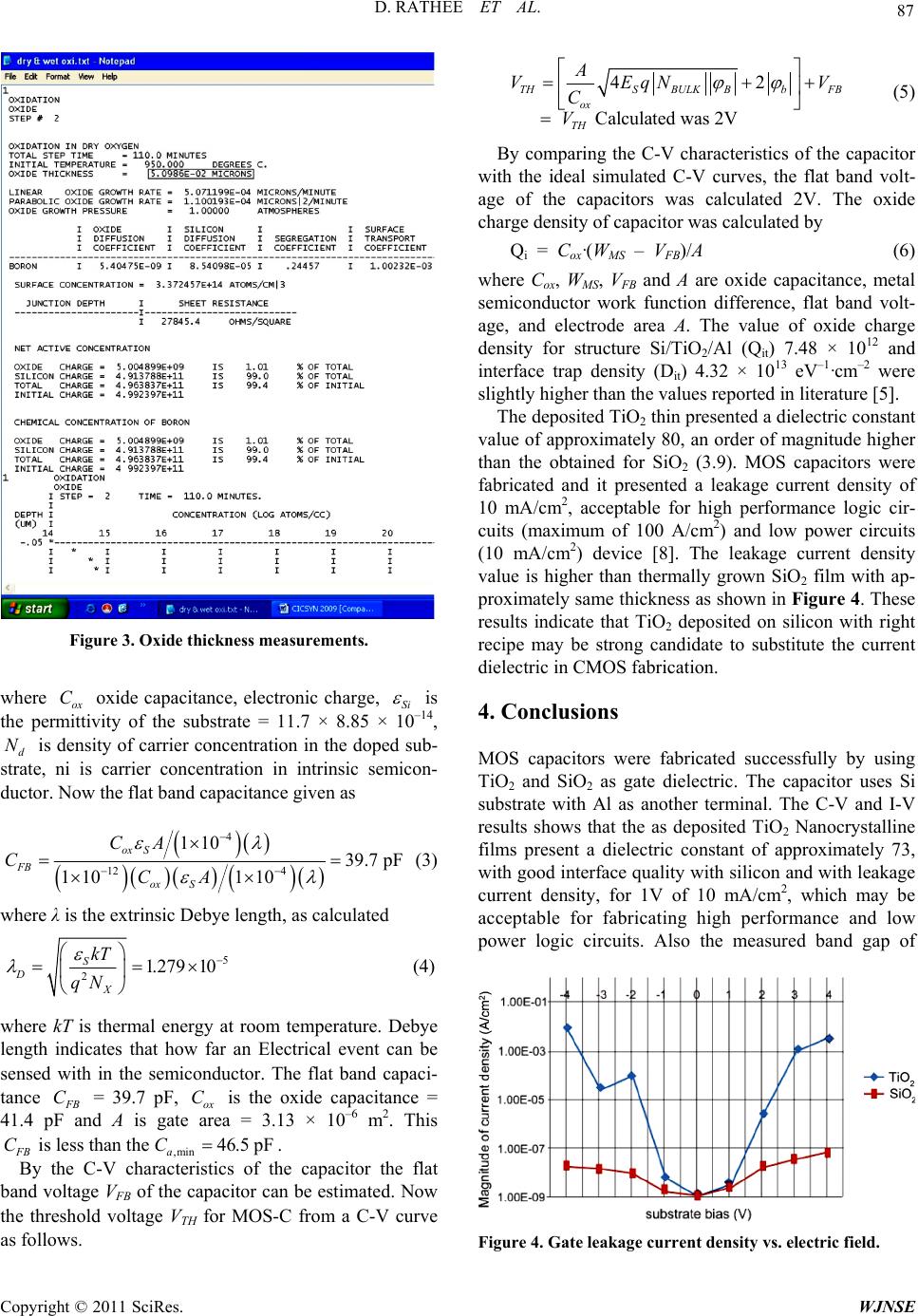
800 micron thick N-type silicon wafer. The dielectric
layer of 510 Å was grown on silicon wafer by dry oxida-
tion at 950˚C for 2 hours. About 3000 Å of aluminum
was then deposited over oxide layers using the sputtering
technique. The 10–2 cm2 capacitor contact was defined by
physical mask. The contacts were annealed in gas at-
mosphere H2, & N2 at 350˚C for 25 minutes. The fabri-
cated capacitors electrically tested to characterize the
material and to inspect the device performance. The
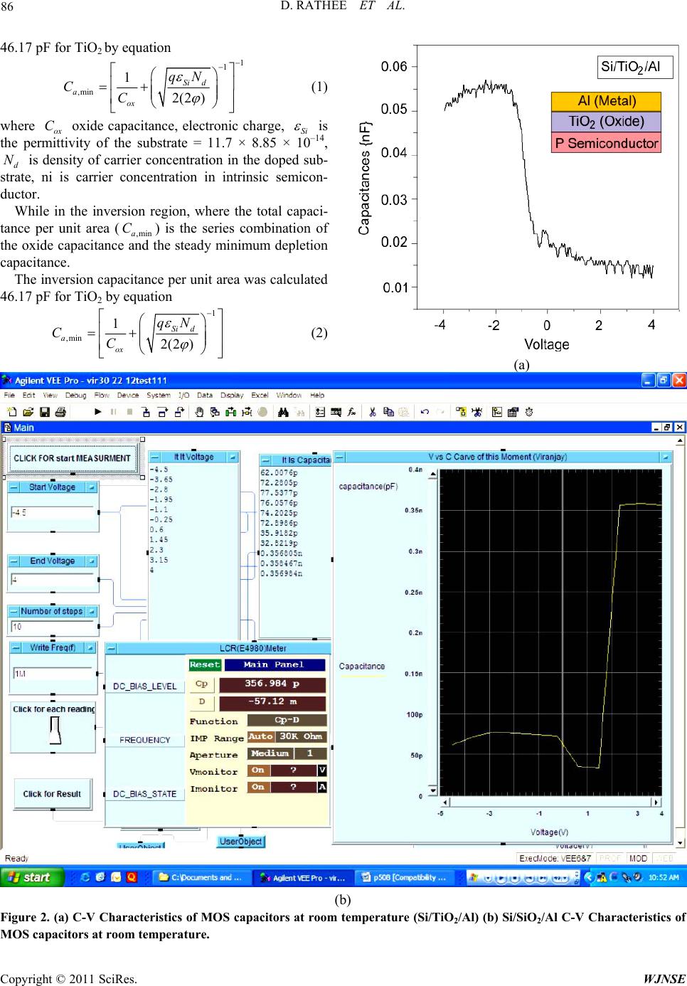
variation of capacitance (C) with voltage VG ranging –5
Volts to +5 Volts is shown in Figure 2.
In this work MOS capacitor were fabricated utilizing
TiO2 film deposited by Sol Gel spin coating method and
SiO2 films were thermally grown on <100> silicon sub-
strate. The C-V measurement for TiO2 was obtained us-
ing C-V analyzer [5,6], while SUPREM-III tool was
used for SiO2 layer. SUPREM- III is a computer program
that allows the user to simulate the various processing
steps used in manufacturing of the Silicon integrated or
discrete devices [7]. The characterization of the samples
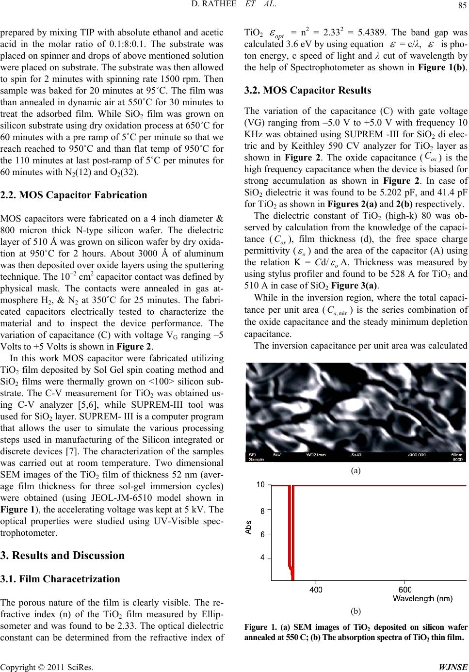
was carried out at room temperature. Two dimensional
SEM images of the TiO2 film of thickness 52 nm (aver-
age film thickness for three sol-gel immersion cycles)
were obtained (using JEOL-JM-6510 model shown in
Figure 1), the accelerating voltage was kept at 5 kV. The
optical properties were studied using UV-Visible spec-
trophotometer.
3. Results and Discussion
3.1. Film Characetrization
The porous nature of the film is clearly visible. The re-
fractive index (n) of the TiO2 film measured by Ellip-
someter and was found to be 2.33. The optical dielectric
constant can be determined from the refractive index of
TiO2 opt
= n2 = 2.332 = 5.4389. The band gap was
calculated 3.6 eV by using equation
= c/λ,
is pho-
ton energy, c speed of light and λ cut of wavelength by
the help of Spectrophotometer as shown in Figure 1(b).
3.2. MOS Capacitor Results
The variation of the capacitance (C) with gate voltage
(VG) ranging from –5.0 V to +5.0 V with frequency 10
KHz was obtained using SUPREM -III for SiO2 di elec-
tric and by Keithley 590 CV analyzer for TiO2 layer as
shown in Figure 2. The oxide capacitance () is the
high frequency capacitance when the device is biased for
strong accumulation as shown in Figure 2. In case of
SiO2 dielectric it was found to be 5.202 pF, and 41.4 pF
for TiO2 as shown in Figures 2(a) and 2(b) respectively.
ox
C
The dielectric constant of TiO2 (high-k) 80 was ob-
served by calculation from the knowledge of the capaci-
tance (ox ), film thickness (d), the free space charge
permittivity (o
C
) and the area of the capacitor (A) using
the relation K = Cd/ o
A. Thickness was measured by
using stylus profiler and found to be 528 A for TiO2 and
510 A in case of SiO2 Figure 3(a).
While in the inversion region, where the total capaci-
tance per unit area (,mina
C) is the series combination of
the oxide capacitance and the steady minimum depletion
capacitance.
The inversion capacitance per unit area was calculated
(a)
(b)
Figure 1. (a) SEM images of TiO2 deposited on silicon wafer
annealed at 550 C; (b) The absorption spectra of TiO2 t h i n f ilm.
Copyright © 2011 SciRes. WJNSE
D. RATHEE ET AL.
Copyright © 2011 SciRes. WJNSE
86
46.17 pF for TiO2 by equation
1
1
,min 1
2(2 )
Si d
a
ox
qN
CC









(1)
where ox oxide capacitance, electronic charge, Si
C
is
the permittivity of the substrate = 11.7 × 8.85 × 10–14,
d is density of carrier concentration in the doped sub-
strate, ni is carrier concentration in intrinsic semicon-
ductor.
N
While in the inversion region, where the total capaci-
tance per unit area (,mina) is the series combination of
the oxide capacitance and the steady minimum depletion
capacitance.
C
The inversion capacitance per unit area was calculated
46.17 pF for TiO2 by equation
1
,min 1
2(2 )
Si d
a
ox
qN
CC






(2)
(a)
(b)
Figure 2. (a) C-V Characteristics of MOS capacitors at room temperature (Si/TiO2/Al) (b) Si/SiO2/Al C-V Characteristics of
MOS capacitors at room temperature.
87
D. RATHEE ET AL.
Figure 3. Oxide thickness measurements.
where ox oxide capacitance, electronic charge, Si
C
is
the permittivity of the substrate = 11.7 × 8.85 × 10–14,
d is density of carrier concentration in the doped sub-
strate, ni is carrier concentration in intrinsic semicon-
ductor. Now the flat band capacitance given as
N



 


4
12 4
110 39.7 pF
110 110
ox S
FB
ox S
CA
CCA




(3)
where λ is the extrinsic Debye length, as calculated
5
21.279 10
S
D
X
kT
qN




(4)
where kT is thermal energy at room temperature. Debye
length indicates that how far an Electrical event can be
sensed with in the semiconductor. The flat band capaci-
tance
F
B = 39.7 pF, ox is the oxide capacitance =
41.4 pF and A is gate area = 3.13 × 10⁻⁶ m
2. This
.
C
is leC
C
4
,min
By the C-V characteristics of the capacitor the flat
band voltage VFB of the capacitor can be estimated. Now
the threshold voltage VTH for MOS-C from a C-V curve
as follows.
ss than the 6.5p F
FB a
C
42
Calculated was 2V
THSBULK BbFB
ox
TH
A
VEqN
C
V





V
(5)
By comparing the C-V characteristics of the capacitor
with the ideal simulated C-V curves, the flat band volt-
age of the capacitors was calculated 2V. The oxide
charge density of capacitor was calculated by
Qi = Cox·(WMSVFB)/A (6)
where Cox, WMS, VFB and A are oxide capacitance, metal
semiconductor work function difference, flat band volt-
age, and electrode area A. The value of oxide charge
density for structure Si/TiO2/Al (Qit) 7.48 × 10¹² and
interface trap density (Dit) 4.32 × 10¹³ eV–1·cm–2 were
slightly higher than the values reported in literature [5].
The deposited TiO2 thin presented a dielectric constant
value of approximately 80, an order of magnitude higher
than the obtained for SiO2 (3.9). MOS capacitors were
fabricated and it presented a leakage current density of
10 mA/cm2, acceptable for high performance logic cir-
cuits (maximum of 100 A/cm2) and low power circuits
(10 mA/cm2) device [8]. The leakage current density
value is higher than thermally grown SiO2 film with ap-
proximately same thick ness as shown in Figure 4. These
results indicate that TiO2 deposited on silicon with right
recipe may be strong candidate to substitute the current
dielectric in CMOS fabrication.
4. Conclusions
MOS capacitors were fabricated successfully by using
TiO2 and SiO2 as gate dielectric. The capacitor uses Si
substrate with Al as another terminal. The C-V and I-V
results shows that the as deposited TiO2 Nanocrystalline
films present a dielectric constant of approximately 73,
with good interface quality with silicon and with leakage
current density, for 1V of 10 mA/cm2, which may be
acceptable for fabricating high performance and low
power logic circuits. Also the measured band gap of
Figure 4. Gate leakage current density vs. electric field.
Copyright © 2011 SciRes. WJNSE
D. RATHEE ET AL.
88
TiO2 thin film was 3.6 eV may be applied in microelec
tronics applications. The higher value of leakage current
density and interface trap density of MOS capacitors
requires further improvement in the deposition process.
The measured results shows that thermally grown oxide
has desirable properties in terms of leakage current and
interface trap density but another obtained parameter like
higher dielectric constant and small band gap are also
considerable. More research is needed in case of TiO2 to
solve leakage current problem without decreasing in ef-
fective dielectric constant.
5. Acknowledgements
The author would like to thank Prof. G. Singh and Mr
Virenjay M Shrivastava, both from Deaprtment of Elec-
tronics and Communicatio n Engineering, Jaypee Univer-
sity of Information Technology, Solan, India, who permit
to take the reference of their work related to Silicon
Technology. The author also wants to thank Dr. K. S.
Yadav, Sr. Scientist, CEERI, Pilani, India for many in-
sightful d i s cussions.
6. References
[1] S. A. Campbell, D. C. Glimer, X. C. Wang, M. Hsieh, H.
S. Kim, et al., “MOSFET Transistor Fabricated with
High Permittivity TiO2 Dielectric,” IEEE Transactions
Electron Devices, Vol. 44, No. 1, 1997, pp. 104-109.
doi:10.1109/16.554800
[2] S. K. Samanta, S. Chatterjee, L. K. Bera and H. D. Baner-
jee, “Temperature Dependence of Electrical Properties of
N2O/O2/N2O Grown Oxide on Strained SiGe,” Applied
Physics Letters, Vol. 80, No. 14, 2002, pp. 2547-2549.
doi:10.1063/1.1469221
[3] S. K. Ray, D. W. Mc Neil, D. L. Gay, C. K. Marti, G. A.
Armstrong and B. M. Armstrong, “Composition of Si1-yCy
Films Produced by Solid-Phase Epitaxy and Rapid Ther-
mal Vapour Deposition,” Thin Solid Films, Vol. 294, No.
1-2, 1997, pp. 149-152.
doi:10.1016/S0040-6090(96)09389-3
[4] H. Iwai and H. Wong, “On the Scaling Issues and High-J
Replacement of Ultrathin Gate Dielectrics for Nanoscale
MOS Transistors,” Microelectronic Engineering, Vol. 83,
2006, pp. 1867-1904.
[5] E. H. Nicollian and J. R. Brew, MOS Physics and Tech-
nology, John Wiley& Sons, New York, 1982.
[6] S. M. Sze, Physics of Semiconductor Devices, 2nd Edi-
tion, Wiley, New York, 1985.
[7] A. I. Akinwande, “IC Lab Testing,” unpublished.
[8] B. G. Streetman, Solid State Electronics Devices, 1995.
[9] V. M. Srivastava, G. Singh and K. S. Yadav, “Measure-
ment of Oxide Thickness for MOS Devices, Using Simu-
lation of SUPREM Simulator,” International Journal of
Recent Trends in Engineering, Vol. 1, No. 4, 2009.
[10] M. Kumar and D. Kumar, “The Deposition of Nanocrys-
talline TiO2 Thin Film on Silicon Using Sol-Gel Tech-
nique and its Characterization,” Microelectronic Engi-
neering, Vol. 87, No. 3, 2010, pp. 447-450.
doi:10.1016/j.mee.2009.08.025
Copyright © 2011 SciRes. WJNSE