World Journal of Nano Science and Engineering, 2011, 1, 73-78
doi:10.4236/wjnse.2011.13011 Published Online September 2011 (http://www.SciRP.org/journal/wjnse)
Copyright © 2011 SciRes. WJNSE
Analysis of Cr Atoms Three-Dimensional
Deposition Characteristics*
Hua-Lei Yang, Wen-Tao Zhang, Jian Yang
Department of Electrical Engineering and Automation, Guilin University of Electronic Technology, Guilin, China
E-mail: mnvad@163.com
Received July 23, 2011; revised August 9, 2011; accepted August 16, 2011
Abstract
The semi-classical model is used to simulate the three-dimensional trajectory and deposition distribution of
the chromium atoms in the Gaussian laser standing wave field using the Runge-Kutta method, and then the
three-dimensional deposition stripes are also given, besides, the effects of atomic beam divergence, chro-
matic aberration and spherical aberration on deposition structure are also analyzed.
Keywords: Three-Dimensional Analysis, Atom Deposition, Cr Atoms, Gaussian Laser Standing Wave Field
1. Introduction
Nanotechnology is one of the fastest growing, most ex-
tensively studied, and putting up the most in the territory
of science and technology currently, and it is known as
the 21st-century science. Its purpose is to “research, develop
and process those materials, devices and systems whose
construction sizes are smaller than 100 nanometers in
order to obtain the required functionality and perfor-
mance [1]”. This definition covers the process of nano-
fabrication, designs, characteristics and shapes of nano-
structures, and measurement and characterization methods
of nano-scale.
Nanometer measurement plays an irreplaceable im-
portant role in information collection and analysis of the
nanotechnology. Nanometrology is involved with the in-
tervals and displacements of the measurement objects
within the range of 0.1 nm - 100 nm, the features of ob-
jects and their surface morphology, the development of
technology and instrument of nano-micro-electronics,
micro-machinery and precision measurement, the re-
search on the interaction of probe and measured surface
during nano-measurement as well as structures and in-
tervention calibration methods of nano-devices. In order
to achieve the calibration of nano-test-equipments in
working sites or general laboratories, a good nano-scale
length transfer standard is needed.
Therefore, to develop accurate and applicable nano-
transfer standard is the present urgent problem and re-
search priorities. Its technical routes are mainly along
three directions, and one of it is laser focused atomic
deposition for Nanometer-scale structure. In NIST, Mc-
Clelland et al. once obtained one-dimensional optical
gratings of chromium using laser focused atomic de-
position technique, the uncertainty of average pitch of
focused atomic deposition process manufacturing stand-
ard sample was 0.0049 nm [2]. In February 1998, the
average pitch of Cr sample which was fabricated by
NIST and deposited on Sapphire was 212.7787 ± 0.0049
nm (The substrate temperature was 29˚C) [3]. And then
in 2002, the average pitch measured by optical diff-
raction was confirmed to be 212.7777 ± 0.0069 nm [4].
This was in good line with the expected pitch 212.7705 ±
0.0049 nm at 22˚C [4]. The uncertainty of this average
pitch was 10–5, which can be directly traced to the
absolute atomic transition frequency. Therefore, the pro-
duced nano-grating structures are very accurate, and are
accordance with the requirements of nano-transfer stan-
dard.
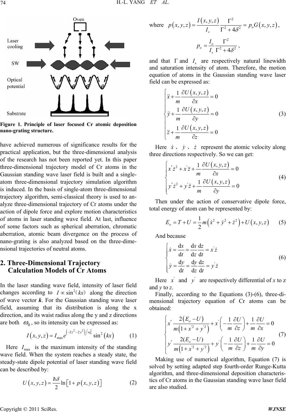
The basic principle of laser focused atomic deposition
for nanostructure is that uses radiation pressure of reso-
nant laser standing wave field to make density of atoms’
high-collimated beam to generate periodic distribution in
space, and then these neutral atoms are deposited on a
substrate to form nano-scale grating structures. Figure 1
shows the schematic of laser focused atomic deposition
for nano-grating structure.
For theoretical analysis of the laser focused atomic
deposition for nano-grating, some research teams both at
home and abroad have done one-dimensional and two-
dimensional simulations for different neutral atoms, and
*Supported by the National Natural Science Foundation of China unde
Grant Number 11064002 and 11061011.