V. M. SRIVASTAVA ET AL.
599
“Automation of Photoacoustic Spectrometer Using VEE
Pro Software,” Journal of Measurement, Vol. 43, No. 10,
2010, pp. 1336-1344.
doi:10.1016/j.measurement.2010.07.011
[8] V. M. Srivastava, K. S. Yadav and G. Singh, “Analysis of
Double Gate CMOS for Double-Pole Four-Throw RF
Switch Design at 45-nm Technology,” Journal of Com-
putational Electronics, Vol. 10, No. 1-2, June 2011, pp.
229-240. doi:10.1007/s10825-011-0359-6
[9] P. Mekanand and D. Eungdamorang, “DP4T CMOS
Switch in a Transceiver of MIMO System,” Proceedings
of 11th IEEE International Conference of Advanced
Communication Technology, Gangwon-Do, 15-18 Febru-
ary 2009, pp. 472-474.
[10] V. M. Srivastava, K. S. Yadav and G. Singh, “Design and
Performance Analysis of Cylindrical Surrounding Dou-
ble-Gate MOSFET for RF Switch,” Microelectronics
Journal, Vol. 42, No. 10, October 2011, pp. 1124-1135.
doi:10.1016/j.mejo.2011.07.003
[11] P. H. Woerlee, M. J. Knitel and A. J. Scholten, “RF
CMOS Performance Trends,” IEEE Transactions on
Electron Devices, Vol. 48, No. 8, 2001, pp. 1776-1782.
doi:10.1109/16.936707
[12] V. M. Srivastava, K. S. Yadav and G. Singh, “Design and
Performance Analysis of Double-Gate MOSFET over
Single-Gate MOSFET for RF Switch,” Microelectronics
Journal, Vol. 42, No. 3, March 2011, pp. 527-534.
doi:10.1016/j.mejo.2010.12.007
[13] M. Popa and R. Ionel, “Virtual Instrumentation Applica-
tion for System Identification,” Proceedings of IEEE In-
strumentation and Measurement Technology Conference,
Sorrento, 24-27 April 2006, pp. 842-846.
doi:10.1109/IMTC.2006.328215
[14] J. Brews, “An Improved High-Frequency MOS Capaci-
tance Formula,” Journal of Applied Physics, Vol. 45, No.
3, June 1974, pp. 1276-1279. doi:10.1063/1.1663401
[15] G. Panigrahi “Numerical Calculation of Low Frequency
Capacitance/Voltage Curves of MOS Capacitor with
Nonconstant Doping Profiles,” Electronics Letters, Vol. 9,
No. 2, Jan 1973, pp. 43-45. doi:10.1049/el:19730030
[16] T. J. Mego, “Guidelines for Interpreting CV Data,” Solid
State Technology, Vol. 33, No. 5, May 1990, pp. 159-
163.
[17] S. M. Sze, “Physics of Semiconductor Devices,” 2nd
Edition, Wiley, New York, 1985.
[18] E. H. Nicollian and J. R. Brews, “MOS Physics and
Technology,” Wiley, New York, 1982.
[19] Y. Cheng and M. Matloubian, “Frequency Dependent
Resistive and Capacitive Components in RF MOSFETs,”
IEEE Electron Device Letters, Vol. 22, No. 7, July 2001,
pp. 333-335. doi:10.1109/55.930682
[20] N. Weste and D. Harris, “CMOS VLSI Design: A Cir-
cuits and Systems Perspective,” 3rd Edition, Pearson Ad-
dison Wesley, Boston, 2005.
[21] M. Fragopoulou, S. Siskos, M. Manolopoulou, M. Zamani
and G. Sarrabayrouse, “Thermal Neutron Dosimetry Us-
ing MOSFET Dosemeters,” Journal of Radiation Meas-
urement, Vol. 44, No. 9-10, 2009, pp. 1006- 1008.
[22] S. K. Ghandhi, “VLSI Fabrication Principles: Silicon and
Gallium Arsenide,” 2nd Edition, Wiley, New Delhi, 2004.
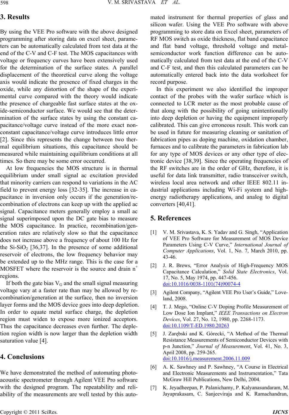
[23] V. M. Srivastava, K. S. Yadav and G. Singh, “Measurement
of Oxide Thickness for MOS Devices, Using Simulation
of SUPREM Simulator,”International Journal of Computer
Applications, Vol. 1, No. 6, March 2010, pp. 66-70.
[24] A. Srivastava, P. Sarkar and C. K. Sarkar, “Study of Gate
Dielectric Permittivity Variation with Different Equiva-
lent Oxide Thickness on Channel Engineered Deep Sub-
Micrometer N-MOSFET Device for Mixed Signal Ap-
plications,” Microelectronics Reliability, Vol. 49, No. 4,
April 2009, pp. 365-370.
doi:10.1016/j.microrel.2008.11.008
[25] J. He, X. Zhang and Y. Y. Wang, “Modeling of MOSFET
Surface Capacitance Behavior under Non-equilibrium,”
IEEE Solid State Electronics, Vol. 50, No. 2, 2006, pp.
259-262. doi:10.1016/j.sse.2005.12.008
[26] T. H. Lee, “The Design of CMOS Radio Frequency Inte-
grated Circuits,” 2nd Edition, Cambridge University
Press, Cambridge, 2004.
[27] R. Biberger, G. Benstetter, H. Goebel and A. Hofer, “In-
termittent-Contact Capacitance Spectroscopy—A New
Method for Determining C-V Curves with Sub-Micron
Lateral Resolution,” Journal of Microelectronics Reliabil-
ity, Vol. 50, No. 9-11, 2010, pp. 1511-1513.
doi:10.1016/j.microrel.2010.07.052
[28] S. Kang and Y. Leblebichi, “CMOS Digital Integrated
Circuits Analysis and Design,” 3rd Edition, McGraw-Hill,
New York, 2002.
[29] V. M. Srivastava, K. S. Yadav and G. Singh, “Designing
Parameters for RF CMOS Cells,”Circuits and Systems,
Vol. 1, No. 2, 2010, pp. 49-53.
doi:10.4236/cs.2010.12008
[30] G. K. Yeap and F. N. Najm, “Low Power VLSI Design
and Technology,” Pearson Addison Wesley, 1st Edition,
Boston, 2008.
[31] J. P. Xu, X. Xiao and P. T. Lai, “A Carrier-Mobility
Model for High-K Gate-Dielectric Ge Mosfets with Metal
Gate Electrode,” Microelectronics Reliability, Vol. 50,
No. 8, 2010, pp. 1081-1086.
doi:10.1016/j.microrel.2010.04.016
[32] S. H. Lee, C. S. Kim and H. K. Yu, “A Small Signal RF
Model and Its Parameter Extraction for Substrate Effects
in RF MOSFETs,” IEEE Transactions on Electron De-
vices, Vol. 48, No. 7, July 2001, pp. 1374-1379.
doi:10.1109/16.930654
[33] T. Sokollik, “Plasma Physics,” Investigations of Field
Dynamics in Laser Plasmas with Proton Imaging, Vol. 1,
2011, pp. 17-24. doi:10.1007/978-3-642-15040-1_3
[34] G. Katti, M. Stucchi, K. Meyer and W. Dehaene, “Elec-
trical Modeling and Characterization of Through Silicon
via for Three-Dimensional ICs,” IEEE Transactions on
Electron Devices, Vol. 57, No. 1, 2010, pp. 256-262.
doi:10.1109/TED.2009.2034508
Copyright © 2011 SciRes. IJCNS