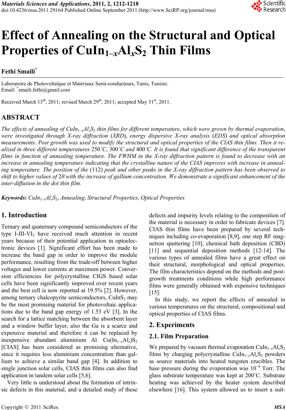
 Materials Sciences and Applications, 2011, 2, 1212-1218 doi:10.4236/msa.2011.29164 Published Online September 2011 (http://www.SciRP.org/journal/msa) Copyright © 2011 SciRes. MSA Effect of Annealing on the Structural and Optical Properties of CuIn1–xAlxS2 Thin Films Fethi Smaili* Laboratoire de Photovoltaïque et Matériaux Semi-conducteurs, Tunis, Tunisie. Email: *smaili.fethi@gmail.com Received March 13th, 2011; revised March 29th, 2011; accepted May 31st, 2011. ABSTRACT The effects of annealing of CuIn1 xAlxS2 thin films for different temperature, which were grown by thermal evaporation, were investigated through X-ray diffraction (XRD), energy dispersive X-ray analysis (EDS) and optical absorption measurements. Post growth was used to modify the structural and optical properties of the CIAS thin films. Then it re- alized in three different temperatures 250˚C, 300˚C and 400˚C. It is found that significant difference of the transparent films in function of annealing temperature. The FWHM in the X-ray diffraction pattern is found to decrease with an increase in annealing temperature indicating that the crystalline nature of the CIAS improves with increase in anneal- ing temperature. The position of the (112) peak and other peaks in the X-ray diffraction pattern has been observed to shift to higher values of 2θ with the increase of gallium concentration. We demonstrate a significant enhancement of the inter-diffusion in the dot thin film. Keywords: CuIn1–xAlxS2, Annealing, Structural Properties, Optical Properties 1. Introduction Ternary and quaternary compound semiconductors of the type I-III-VI2 have received much attention in recent years because of their potential application in optoelec- tronic devices [1]. Significant effort has been made to increase the band gap in order to improve the module performance, resulting from the trade-off between higher voltages and lower currents at maximum power. Conver- sion efficiencies for polycrystalline CIGS based solar cells have been significantly improved over recent years and the best cell is now reported at 19.5% [2]. However, among ternary chalcopyrite semiconductors, CuInS2 may be the most promising material for photovoltaic applica- tions due to the band gap energy of 1.53 eV [3]. In the search for a lattice matching between the absorbent layer and a window buffer layer, also the Ga is a scarce and expensive material and therefore it can be replaced by inexpensive abundant aluminium Al. Cu(In1xAlx)S2 [CIAS] has been considered as promising alternative, since it requires less aluminium concentration than gal- lium to achieve a similar band gap [4]. In addition to single junction solar cells, CIAS thin films can also find application in tandem solar cells [5,6]. Very little is understood about the formation of intrin- sic defects in this material, and a detailed study of these defects and impurity levels relating to the composition of the material is necessary in order to fabricate devices [7]. CIAS thin films have been prepared by several tech- niques including co-evaporation [8,9], one step RF mag- netron sputtering [10], chemical bath deposition (CBD) [11] and sequential deposition methods [12-14]. The various types of annealed films have a great effect on their structural, morphological and optical properties. The film characteristics depend on the methods and post- growth treatments conditions while high performance films were generally obtained with expensive techniques [15]. In this study, we report the effects of annealed in various temperatures on the structural, compositional and optical properties of CIAS films. 2. Experiments 2.1. Film Preparation We prepared by vacuum thermal evaporation CuIn1–xAlxS2 films by charging polycrystalline CuIn1xAlxS2 powders as source materials into heated tungsten crucibles. The base pressure during the evaporation was 106 Torr. The glass substrate temperature was kept at 200˚C. Substrate heating was achieved by the heater system described elsewhere [16]. This system allowed us to insert a suit- 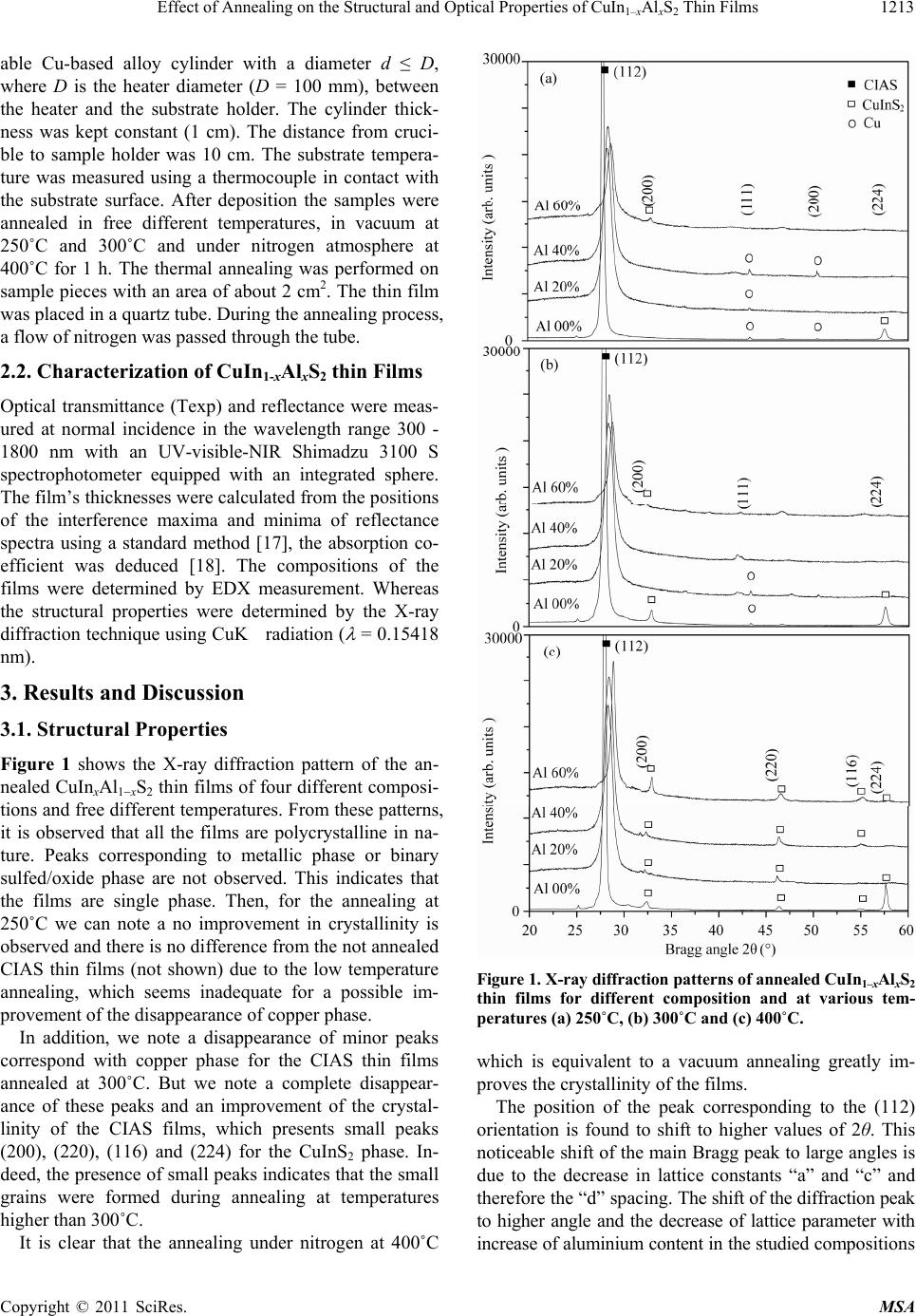 Effect of Annealing on the Structural and Optical Properties of CuInAl S Thin Films1213 1–xx 2 able Cu-based alloy cylinder with a diameter d ≤ D, where D is the heater diameter (D = 100 mm), between the heater and the substrate holder. The cylinder thick- ness was kept constant (1 cm). The distance from cruci- ble to sample holder was 10 cm. The substrate tempera- ture was measured using a thermocouple in contact with the substrate surface. After deposition the samples were annealed in free different temperatures, in vacuum at 250˚C and 300˚C and under nitrogen atmosphere at 400˚C for 1 h. The thermal annealing was performed on sample pieces with an area of about 2 cm2. The thin film was placed in a quartz tube. During the annealing process, a flow of nitrogen was passed through the tube. 2.2. Characterization of CuIn1-xAlxS2 thin Films Optical transmittance (Texp) and reflectance were meas- ured at normal incidence in the wavelength range 300 - 1800 nm with an UV-visible-NIR Shimadzu 3100 S spectrophotometer equipped with an integrated sphere. The film’s thicknesses were calculated from the positions of the interference maxima and minima of reflectance spectra using a standard method [17], the absorption co- efficient was deduced [18]. The compositions of the films were determined by EDX measurement. Whereas the structural properties were determined by the X-ray diffraction technique using CuK radiation ( = 0.15418 nm). 3. Results and Discussion 3.1. Structural Properties Figure 1 shows the X-ray diffraction pattern of the an- nealed CuInxAl1xS2 thin films of four different composi- tions and free different temperatures. From these patterns, it is observed that all the films are polycrystalline in na- ture. Peaks corresponding to metallic phase or binary sulfed/oxide phase are not observed. This indicates that the films are single phase. Then, for the annealing at 250˚C we can note a no improvement in crystallinity is observed and there is no difference from the not annealed CIAS thin films (not shown) due to the low temperature annealing, which seems inadequate for a possible im- provement of the disappearance of copper phase. In addition, we note a disappearance of minor peaks correspond with copper phase for the CIAS thin films annealed at 300˚C. But we note a complete disappear- ance of these peaks and an improvement of the crystal- linity of the CIAS films, which presents small peaks (200), (220), (116) and (224) for the CuInS2 phase. In- deed, the presence of small peaks indicates that the small grains were formed during annealing at temperatures higher than 300˚C. It is clear that the annealing under nitrogen at 400˚C Figure 1. X-r ay dif fr a ct i on pa t t e r ns of anneale d CuIn1–xAlxS2 thin films for different composition and at various tem- peratures (a) 250˚C, (b) 300˚C and (c) 400˚C. which is equivalent to a vacuum annealing greatly im- proves the crystallinity of the films. The position of the peak corresponding to the (112) orientation is found to shift to higher values of 2θ. This noticeable shift of the main Bragg peak to large angles is due to the decrease in lattice constants “a” and “c” and therefore the “d” spacing. The shift of the diffraction peak to higher angle and the decrease of lattice parameter with increase of aluminium content in the studied compositions Copyright © 2011 SciRes. MSA  Effect of Annealing on the Structural and Optical Properties of CuIn1–xAlxS2 Thin Films Copyright © 2011 SciRes. MSA 1214 cherrer equation [19]: are in accordance to Vegards law [1]. These results indi- cate that CIAS solid solution has been successfully ob- tained without any phase separation into CIS or CAS or any other secondary phases. We here with report and dis- cuss the structural parameters of the CIAS thin films. 0.9 cos DB (1) where is the x-ray wavelength, is the Bragg diffrac- tion angle, and B is the full-width at half-maximum (FWHM) of the peak corresponding to . When calcu- lated by using the peak corresponding to the (112) plane of CIAS. Figure 2 shows that the average grain size is found to decrease as well as aluminium concentration increase (Table 1). The lattice parameters for the CIAS thin films have been evaluated and are shown in Table 1. The lattice parameter values “a” and “c” are found to decrease as aluminium concentration increases. This may be due to the fact that aluminium atom is smaller in size than in- dium atom and hence causes shrinkage in the lattice as they substitute indium sites in the cell. The FWHM is found to increase as the aluminium concentration in- creases and this can be attributed to the incorporation of the aluminium element in the indium sites, which distorts the normal lattice structure of CuInS2. The observed in- crease in FWHM values corresponds to a decrease in the effective grain size with increased aluminium incorpora- tion into the network parameter of CuInS2. 3.2. Compositional Analysis The chemical constituents present in the thin films have been identified using energy dispersive X-ray analysis. The composition of the CIAS thin films are shown in Table 2. The composition of the CIAS films were tested at four different regions on the film surface and the val- ues reported in Table 2 are an average of the atomic percentage of each element. As can be seen in Table 1, The average crystallite size can be calculated using the Table 1. Structural parameters of CIAS films. Lattice parameter Samples a (Å) c (Å) d 112 (Å) Film thickness (nm) FWHM Grain size (Å) CIAS: Al 00at.% 5.524 11.159 3.1997 480 0.247 320 CIAS: Al 20at.% 5.503 10.723 3.1491 320 0.986 79 CIAS: Al 40at.% 5.496 10.632 3.1375 310 0.992 75 Annealed at 250˚C CIAS: Al 60at.% 5.474 10.421 3.1073 300 0.8232 76 CIAS: Al 00at.% 5.524 11.159 3.1997 440 0.236 340 CIAS: Al 20at.% 5.498 10.712 3.1461 450 0.937 86 CIAS: Al 40at.% 5.492 10.633 3.1361 350 0.982 77 Annealed at 300˚C CIAS: Al 60at.% 5.480 10.348 3.1017 380 0.687 89 CIAS: Al 00at.% 5.524 11.109 3.1949 490 0.177 390 CIAS: Al 20at.% 5.502 10.771 3.1534 460 0.922 92 CIAS: Al 40at.% 5.497 10.686 3.1433 400 0.998 90 Annealed at 400˚C CIAS: Al 60at.% 5.473 10.333 3.0974 460 0.510 102 Table 2. Thin films elemental compositions (at.%). Samples S In Cu Al O Cu In Al Al In Al S Cu In Al Eg CIAS: Al 00at.% 49.91 24.8625.22-- 0 1.01 0.00 1.00 1.47 CIAS: Al 20at.% 49.38 20.0625.154.85 0.111.00 0.19 0.99 1.50 CIAS: Al 40at.% 50.03 16.1724.369.73 0.130.96 0.38 1.00 1.68 Annealed at 250˚C CIAS: Al 60at.% 49.26 11.0525.3614.140.150.95 0.56 0.97 1.98 CIAS: Al 00at.% 50.03 25.1724.76-- 0 0.98 0.00 1.00 1.43 CIAS: Al 20at.% 49.91 19.9625.025.15 0.121.00 0.21 1.00 1.54 CIAS: Al 40at.% 49.56 15.2525.2610.040.131.00 0.40 0.98 1.81 Annealed at 300˚C CIAS: Al 60at.% 50.03 10.5724.3615.130.150.99 0.59 1.00 1.84 CIAS: Al 00at.% 48.91 24.8626.22-- 0 1.05 0.00 0.96 1.45 CIAS: Al 20at.% 49.26 19.2526.365.04 0.141.09 0.21 0.97 1.50 CIAS: Al 40at.% 48.93 15.6725.969.43 0.151.03 0.38 0.96 1.60 Annealed at 400˚C CIAS: Al 60at.% 49.06 9.54 26.1616.040.171.02 0.63 0.95 1.85  Effect of Annealing on the Structural and Optical Properties of CuInAl S Thin Films 1215 1–xx 2 Figure 2. Grain sizes of CuIn1–xAlxS2 thin films versus alu- minum content percent for various temperatures (a) 250˚C, (b) 300˚C and (c) 400˚C. the ratio of Cu, In, Al and S elements in the CIAS film is almost 1: 1: 2. It is seen that the ratio of Cu/(In + Al) is near of the unity and the ratio of S/(Cu + In + Al) is close to unity. In addition, we note an increase in the Al/(In + Al) ratio from 0 to 0.59 which is almost the composition of the used powders. 3.3. Optical Properties 3.3.1. Transmission and Reflection Spectra The optical transmission curves of CIAS thin films for different annealing temperatures are depicted respec- tively in Figure 3 and Figure 4. The samples showed a semitransparent behaviour in the infrared region and the thinnest and lowest Al content CIAS sample presented also a relatively high transmission in the visible spectrum. The transmission spectrums of the CuInS2 thin film show interference pattern with sharp fall of transmittance at the band edge for different annealing temperatures, which is an indication of good crystallinity. However, the trans- missions of other films decrease strongly when the alu- minium percent increase in the materials; this is probably due to the inhomogeneities of the films. In addition, we note a decrease in the transmission values for the CIAS thin films annealed at 250˚C and 300˚C for about 10% and 30% respectively. We explain this decrease after annealing by the substitution of the indium element by the aluminium and the diffused alu- minium from the surface into the volume. Figure 3(c) shows the optical transmission spectra of CIAS films annealed at 400˚C. For CuInS2 film, we point out the presence of the interference fringes due to the multitude reflection phenomena showing homogenous films. Moreover these films exhibit a good transparency Figure 3. Transmission spectra of annealed CuIn1–xAlxS2 thin films for different composition and at various tem- peratures (a) 250˚C, (b) 300˚C and (c) 400˚C. in the visible and infrared regions. Than these interfer- ences disappear when we increase the aluminium content in the CIAS thin films and the transmission values de- crease as a function of the aluminium percent and varies from 70% to 10%, this is probably due to the inhomoge- neities present in the volume and the perturbed relief on Copyright © 2011 SciRes. MSA 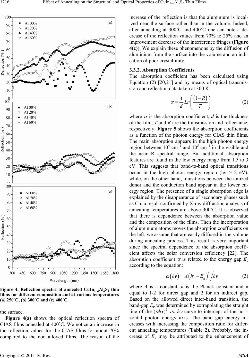 Effect of Annealing on the Structural and Optical Properties of CuInAl S Thin Films 1216 1–xx 2 Figure 4. Reflection spectra of annealed CuIn1xAlxS2 thin films for different composition and at various temperatures (a) 250˚C, (b) 300˚C and (c) 400˚C. the surface. Figure 4(a) shows the optical reflection spectra of CIAS films annealed at 400˚C. We notice an increase in the reflection values for the CIAS films for about 70% compared to the non alloyed films. The reason of the increase of the reflection is that the aluminium is local- ized near the surface rather than in the volume. Indeed, after annealing at 300˚C and 400˚C one can note a de- crease of the reflection values from 70% to 25% and an improvement decrease of the interference fringes (Figure 4(c)). We explain these phenomenons by the diffusion of aluminium from the surface into the volume and an indi- cation of poor crystallinity. 3.3.2. Ab sorption Coefficients The absorption coefficient has been calculated using Equation (2) [20,21] and by means of optical transmis- sion and reflection data taken at 300 K: 1 1R Ln dT (2) where is the absorption coefficient, d is the thickness of the film, T and R are the transmission and reflectance, respectively. Figure 5 shows the absorption coefficients as a function of the photon energy for CIAS thin films. The main absorption appears in the high photon energy region between 104 cm1 and 105 cm1 in the visible and the near-IR spectral range. But additional absorption features are found in the low energy range from 1.5 to 3 eV. This suggests that band-to-band optical transitions occur in the high photon energy region (hν > 2 eV), while, on the other hand, transitions between the ionized donor and the conduction band appear in the lower en- ergy region. The presence of a single absorption edge is explained by the disappearance of secondary phases such as Cu, a result confirmed by X-ray diffraction analysis of annealing temperatures are above 300˚C. It is observed that there is dependence between the absorption value and the composition of the films. Then the incorporation of aluminium atoms moves the absorption coefficients on the left, we assume that are easily diffused in the volume during annealing process. This result is very important since the spectral dependence of the absorption coeffi- cient affects the solar conversion efficiency [22]. The absorption coefficient is related to the energy gap Eg according to the equation: n g hvA hvEhv (3) where A is a constant, h is the Planck constant and n equal to 1/2 for direct gap and 2 for an indirect gap. Based on the allowed direct inter-band transition, the band-gap Eg was determined by extrapolating the straight line of the ( h )2 vs. h curve to intercept of the hori- zontal photon energy axis. The band gap energy in- creases with increasing the composition ratio for differ- ent annealing temperatures (Table 2). Probably, the in- crease of Eg may be attributed to the enhancement of Copyright © 2011 SciRes. MSA 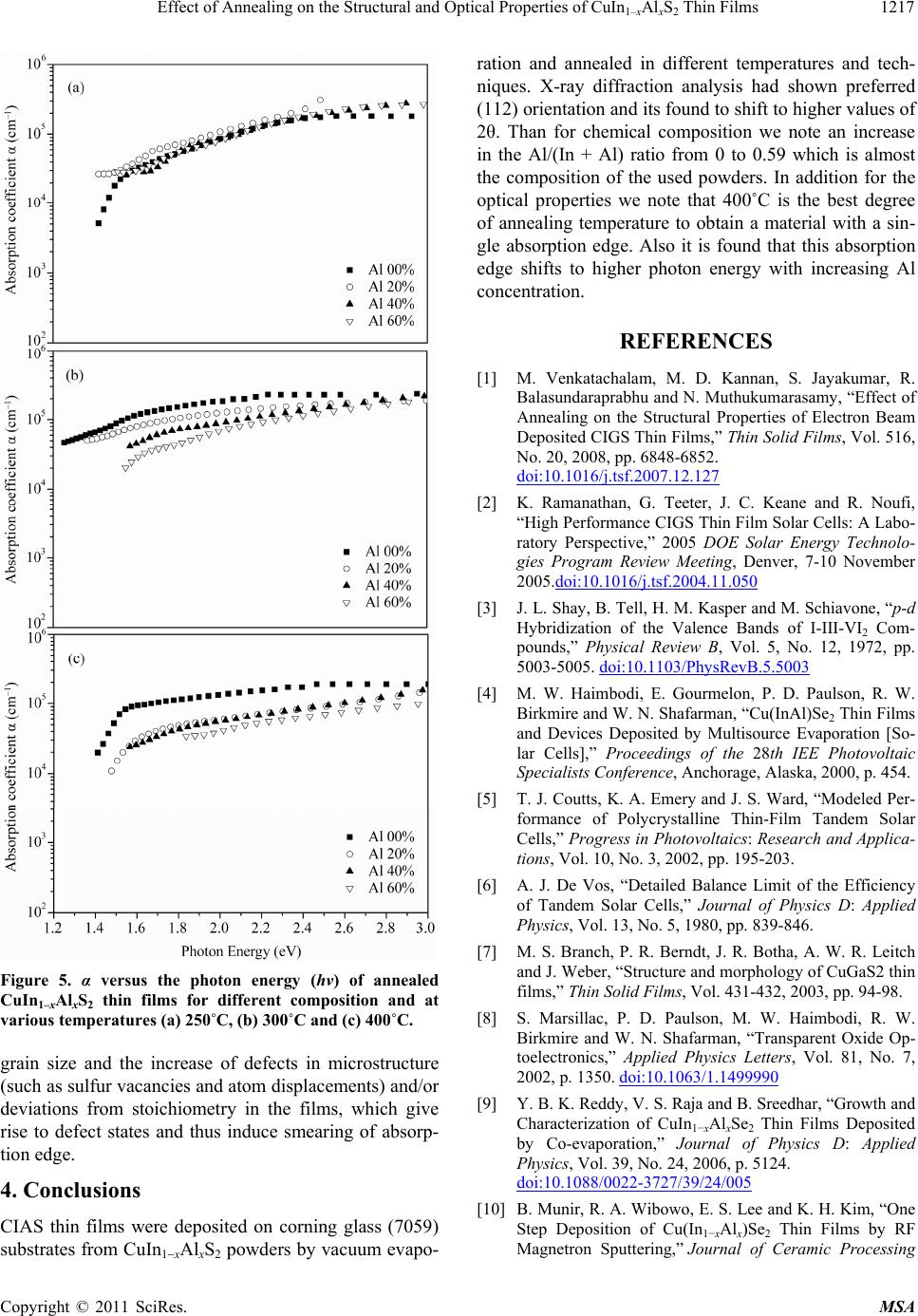 Effect of Annealing on the Structural and Optical Properties of CuInAl S Thin Films1217 1–xx 2 Figure 5. α versus the photon energy (hν) of annealed CuIn1–xAlxS2 thin films for different composition and at various temperatures (a) 250˚C, (b) 300˚C and (c) 400˚C. grain size and the increase of defects in microstructure (such as sulfur vacancies and atom displacements) and/or deviations from stoichiometry in the films, which give rise to defect states and thus induce smearing of absorp- tion edge. 4. Conclusions CIAS thin films were deposited on corning glass (7059) substrates from CuIn1xAlxS2 powders by vacuum evapo- ration and annealed in different temperatures and tech- niques. X-ray diffraction analysis had shown preferred (112) orientation and its found to shift to higher values of 2θ. Than for chemical composition we note an increase in the Al/(In + Al) ratio from 0 to 0.59 which is almost the composition of the used powders. In addition for the optical properties we note that 400˚C is the best degree of annealing temperature to obtain a material with a sin- gle absorption edge. Also it is found that this absorption edge shifts to higher photon energy with increasing Al concentration. REFERENCES [1] M. Venkatachalam, M. D. Kannan, S. Jayakumar, R. Balasundaraprabhu and N. Muthukumarasamy, “Effect of Annealing on the Structural Properties of Electron Beam Deposited CIGS Thin Films,” Thin Solid Films, Vol. 516, No. 20, 2008, pp. 6848-6852. doi:10.1016/j.tsf.2007.12.127 [2] K. Ramanathan, G. Teeter, J. C. Keane and R. Noufi, “High Performance CIGS Thin Film Solar Cells: A Labo- ratory Perspective,” 2005 DOE Solar Energy Technolo- gies Program Review Meeting, Denver, 7-10 November 2005.doi:10.1016/j.tsf.2004.11.050 [3] J. L. Shay, B. Tell, H. M. Kasper and M. Schiavone, “p-d Hybridization of the Valence Bands of I-III-VI2 Com- pounds,” Physical Review B, Vol. 5, No. 12, 1972, pp. 5003-5005. doi:10.1103/PhysRevB.5.5003 [4] M. W. Haimbodi, E. Gourmelon, P. D. Paulson, R. W. Birkmire and W. N. Shafarman, “Cu(InAl)Se2 Thin Films and Devices Deposited by Multisource Evaporation [So- lar Cells],” Proceedings of the 28th IEE Photovoltaic Specialists Conference, Anchorage, Alaska, 2000, p. 454. [5] T. J. Coutts, K. A. Emery and J. S. Ward, “Modeled Per- formance of Polycrystalline Thin-Film Tandem Solar Cells,” Progress in Photovoltaics: Research and Applica- tions, Vol. 10, No. 3, 2002, pp. 195-203. [6] A. J. De Vos, “Detailed Balance Limit of the Efficiency of Tandem Solar Cells,” Journal of Physics D: Applied Physics, Vol. 13, No. 5, 1980, pp. 839-846. [7] M. S. Branch, P. R. Berndt, J. R. Botha, A. W. R. Leitch and J. Weber, “Structure and morphology of CuGaS2 thin films,” Thin Solid Films, Vol. 431-432, 2003, pp. 94-98. [8] S. Marsillac, P. D. Paulson, M. W. Haimbodi, R. W. Birkmire and W. N. Shafarman, “Transparent Oxide Op- toelectronics,” Applied Physics Letters, Vol. 81, No. 7, 2002, p. 1350. doi:10.1063/1.1499990 [9] Y. B. K. Reddy, V. S. Raja and B. Sreedhar, “Growth and Characterization of CuIn1−xAlxSe2 Thin Films Deposited by Co-evaporation,” Journal of Physics D: Applied Physics, Vol. 39, No. 24, 2006, p. 5124. doi:10.1088/0022-3727/39/24/005 [10] B. Munir, R. A. Wibowo, E. S. Lee and K. H. Kim, “One Step Deposition of Cu(In1−xAlx)Se2 Thin Films by RF Magnetron Sputtering,” Journal of Ceramic Processing Copyright © 2011 SciRes. MSA  Effect of Annealing on the Structural and Optical Properties of CuIn1–xAlxS2 Thin Films Copyright © 2011 SciRes. MSA 1218 Research, Vol. 8, No. 4, 2007, p. 252. [11] B. Kavitha and M. Dhanam, “In and Al Composition in Nano-Cu(InAl)Se2 Thin Films from XRD and Transmit- tance Spectra,” Materials Science and Engineering B, Vol. 140, No. 1-2, 2007, pp. 59-63. doi:10.1016/j.mseb.2007.03.011 [12] F. Itoh, O. Saitoh, M. Kita, H. Nagamori and H. Oike, “Growth and Characterization of Cu(InA1)Se2 by Vac- uum Evaporation,” Solar Energy Materials & Solar Cells-Solar Energy, Vol. 50, No. 1-4, 1998, pp. 119-125. doi:10.1016/S0927-0248(97)00132-3 [13] E. Halgand, J. C. Bernède, S. Marsillac and J. Kessler, “Physico-Chemical Characterisation of Cu(In,Al)Se2 Thin Film for Solar Cells Obtained by a Selenisation Process,” Thin Solid Films, Vol. 480-481, 2005, pp. 443446. doi:10.1016/j.tsf.2004.11.039 [14] S. Jost, F. Hergert, R. Hock, M. Purwins and R. Enderle, “Real-Time Investigations of Selenization Reactions in the System Cu-In-Al-Se,” Physica Status Solidi A, Vol. 203, No. 11, 2006, pp. 2581-2587. [15] R. Brini, M. Kanzari, B. Rezig and J. Werckmann, “Ef- fect of Annealing on Properties of CuInS2 Thin Films,” European Physical Journal—Applied Physics, Vol. 30, No. 3, 2005, pp. 153-158. doi:10.1051/epjap:2005031 [16] F. Chaffar Akkari, R. Brini, M. Kanzari and B. Rezig, “High Absorbing CuInS2 Thin Films Growing by Oblique Angle Incidence Deposition in Presence of Thermal Gra- dient,” Journal of Materials Science, Vol. 40, 2005, pp. 1-5. [17] J. Tauc, “Optical Properties of Solids,” North-Holland, Publ., Amsterdam, 1973, p. 277. [18] M. Ben Rabeh, M. Zribi, M. Kanzari and B. Rezig, “Structural and Optical Characterization of Sn Incorpora- tion in CuInS2 Thin Films Grown by Vacuum Evapora- tion Method,” Materials Letters, Vol. 59, No. 24-25, 2005, pp. 3164-3168. doi:10.1016/j.matlet.2005.05.045 [19] H. P. Klug and L. E. Alexander, “X-Ray Diffraction Pro- cedure for Polycrystalline and Amorphous Materials,” Wiley, New York, 1974. [20] D. E. Milovzorov, A. M. Ali, T. Inokuma, Y. Kurata, T. Suzuki and S. Hasegawa, “Optical Properties of Silicon Nanocrystallites in Polycrystalline Silicon Films Prepared at Low Temperature by Plasma-Enhanced Chemical Va- por Deposition,” Thin Solid Films, Vol. 382, No. 1-2, 2001, pp. 47-55. doi:10.1016/S0040-6090(00)01208-6 [21] T. M. Wang, S. K. Zheng, W. C. Hao and C. Wang, “Studies on Photocatalytic Activity and Transmittance Spectra of TiO2 Thin Films Prepared by r.f. Magnetron Sputtering Method,” Surface and Coatings Technology, Vol. 155, No. 2-3, 2002, pp. 141-145. [22] V. V. Kindyak, V. F. Gremenonok, I. V. Bodnar, V. Rud Yu and G. A. Madvedkin, “Optical Properties of La- ser-Evaporated CuGaSe2 Films near and above the Fun- damental Absorption Edge,” Thin Solid Films, Vol. 250, No. 1-2, 1994, pp. 33-36. doi:10.1016/0040-6090(94)90160-0
|