 Materials Sciences and Applicatio ns, 2011, 2, 1205-1211 doi:10.4236/msa.2011.29163 Published Online September 2011 (http://www.SciRP.org/journal/msa) Copyright © 2011 SciRes. MSA 1205 Influence of Defects on Low Temperature Diffusion of Boron in SiC Ilkham G. Atabaev1, Tojiddin M. Saliev1, Dilmurad Saidov1, Vadim A. Pak1, Khimmatali Juraev1, Chin-Che Tin2, Bakhtiyar G. Atabaev3, Vyacheslav N. Giryansky3 1Physical Technical Institute of Uzbek Academy of Sciences, Tashkent, Uzbekistan; 2Department of Physics, Auburn University, Alabama, USA; 3Arifov Institute of Electronics, Uzbek Academy of Sciences, Tashkent, Uzbekistan. Email: atvi@uzsci.net, cctin@physics.auburn.edu, Received January 18th, 2011; revised March 17th, 2011; accepted May 30th, 2011. ABSTRACT The low temperature diffusion of Boron in bulk SiC crystals is investigated and simplified model of such diffusion is presented. The method of UV stim ulated etching by a queous solution of KO H is proposed and some exp erimental data on influence of defects on quality of prepared p-n junctions are presented. Keywords: Diffusion, Activation Energy, Silico ne Carbide, Annealing, Vacancy 1. Introduction Due to its unique material properties, silicon carbide (SiC) is very prospective material for fabrication of high power, high temperature electronic devices that can operate in harsh environment. One of the constraining factors in the fabrication of silicon carbide devices is the necessity of using high temperature of about 1800˚C - 2200˚C to in- troduce impurity by thermal diffusion. Due to the rela- tively low melting temperature of silicon (1412˚C), con- ventional high temperature diffusion of shallow impuri- ties in SiC epilayers grown on Si is impossible. In the case of doping by ion implantation, a post-implantation dopant activation annealing at ~1600˚C is needed. High- temperature thermal processing can cause surface dete- rioration resulting in poor device characteristics. There- fore, a reduction in processing temperature for impurity introduction in SiC is important. To reduction of temperature of diffusion of impurity in SiC up to 1250˚C - 1 300˚C we are proposed and investi- gated new method of low-temperature diffusion of boron [1-4]. In this method, on surface of SiC crystal creates a layer of borosilicate glass, then sample annealed in air. As we have expected, in these conditions, there is the flow of carbon vacancies, which allows to reduce the temperature of diffusion. Experiments have shown that the temperature of diffusion decreased to 1150˚C - 1250˚C. Boron concentration reached a high value to the 1020–21 cm–3. Although this technique has been demonstrated to be applicable to the fabrication of SiC devices [4], further work needs to be done to optimize the technique in order to improve the surface morphology and reduce crystal- line defects and to improve p-n junction characteristics. To achieve these goals, further research of mechanism of low-temperature diffusion of boron is necessary. As mentioned above, we have assumed that on the surface of SiC crystal a flow of carbon vacancies creates. In this case, the diffusion area is saturated by carbon vacancies and the reducing of diffusion temperature related with interaction of impurity with VC. However, it seen from experiments, a significant part of Boron atoms after dif- fusion was in the electrically active state in the silicon sublattice of SiC. It means that during the diffusion con- centration of VSi vacancies should be large. Concentra- tion of Boron was also very high! Thus the need to find out—how occurs the large concentration of silicon va- cancies during low-temperature dif fusion. In the defect enhanced diffusion the method of proc- essing the crystal surface is very important. It is always important, but in our case, diffusion is stimulated by de- fects (VC, VSi, VSiC) that interact with structural defects. So, the quality of the crystal surface in our method has played a key role. That is why it is necessary to conduct our research together with the study of etching of the crystal. In a previous article [4] the results of research carried out on SiC/Si and SiC/SiC structures were presented. In  Influence of Defects on Low Temperature Diffusion of Boron in SiC 1206 this paper, we report on the simplified model of low- temperature diffusion of impurity in bulk SiC crystals, some experimental data on etching and influence of sur- face morphology on IV characteristics are presented. 2. Experimental Results and Discussion 2.1. Physical Approaches for the Implementation of Low-Temperature Diffusion It is well known that mobile point defects play an impor- tant role in diffusion processes in semiconductors. And to reduce the temperature of diffusion the increased con- centration of mobile point defects can be used. One of the possible ways of introducing point defects in crystal is the irradiation of samples during diffusion process. In [5] described the results of studies of radiation- stimulated diffusion of boron in silicon and silicon car- bide irradiated with protons. It is shown that in silicon the temperature of diffusion falls, however, in silicon carbide does not. As shown in [5] a significant decrease in temperature diffusion of cesium (up to temperatures of 1150˚C - 1300˚C) occurs when the amorphization of SiC samples. Of course, this path can not be regarded as op- timal for the manufacturing technology of semicon ductor devices. On our opinion, the surface oxidation of silicon car- bide is a next possible way to effective introduction of point defects (vacancies) in the crystal. Our method of diffusion [1-4] was a modification of the surface oxida- tion. We then assumed that the crystal surface of silicon carbide is formed vacancy flux of carbon. However, we recently found a great article of S. C. Singhal on oxida- tion kinetics of silicon carb ide [6]. In this work [6] is described that at temperatures 1100˚C - 1400˚C SiC exhibits two types of oxidation behavior, “active” and “passive”, depending upon the ambient oxygen potential. At high oxygen pressures, “passive” oxidation occurs wherein a protective film of SiO2(s) is formed on the surface by the reaction: (1) 22 2SiC(s)3O (g)2SiO (s)2CO(g) At low oxygen potentials, severe “active” oxidation occurs due to the formation of gaseous products accord- ing to reactions: 2 SiC(s)2SiO (s)3SiO(g)CO(g) (2) 2 SiC(s) O(g)SiO(g) CO(g) (3) Active oxidation of SiC occurs only at oxygen pres- sures lower than ~3·10–4 atm at 1400˚C. As seen from Equations (2-3) surface oxidation of silicon carbide in this co nditions lead s to produ ction flow of both as Carbon an d Silicon vacancies from th e surface into the bulk of the crystal (May be mostly of carbon vacancies). Obviously, the vacancy concentration in this case can be much higher as compared with the introduc- tion of vacancies by irradiation. 2.2. Distribution of Boron Impurity in Samples after Low—Temperature Diffusion The diffusion of Boron in SiC was performed in non- equilibrium conditions in the flow of vacancies from the surface into volume of crystal using the method de- scribed in [1,2]. In this low-temperature diffusion tech- nique, a thin film of borosilicate glass is created on the surface of a silicon carbide sample. Then sample is an- nealed in the air. Temperature of diffusion was different between 1150˚C and 1300˚C. The distribution of B in the SiC/SiC samples was measured by spreading current method. In this method, the samples were polished by diamond paste at a gradient of 1 - 3 degrees to the surface of the SiC crystal. Then the distribution of specific resistance along the surface of the SiC film was measured to obtain the distribution pro- file of boron, NB(x). Diffusion in crystals of silicon carbide of various polytypes was carried out as well. Since diffusion is stimulated by defects the inhomogeneity of the distribu- tion of impurities and defects in the crystals play an im- portant role. As a result, the surface and depth distribu- tion of impurity in p-area is nonun iform. Figure 1 shows the distribution of the impurity measured in different points of the 3C-SiC crystal and distribution of Boron in 4H-SiC. Estimates have shown that for bulk crystals of silicon carbide activation energy of diffusion Ea~ 0.9 - 1.2 eV as was determined in experiments with SiC/SiC het- erostructures in [4]. 2.3. Some Remarks on Possible Mechanism of Low-Temperature Diffusion of Boron In our previous work [4], based on an analysis of litera- ture on diffusion mechanisms in SiC [7-11] has been assumed that the accelerated diffusion takes place via mobile (Bc-Vc) associates. However, according to expressions (2,3) silicon va- cancy are also formed on the surface of the crystal. Thus it can be assumed that the diffusion of impurities goes via Si and C vacancies at different rates and as described in [8] with a different solubility in Si and C-sublattices. To test this hypothesis in samples without the boro- silicate glass layer a boron diffusion was performed in vacuum with low oxygen pressure (as in work [6]). After diffusion at 1200˚C in SiC crystal the p-type layer was created. Thus, according to expressions (2,3) a flow of Vc and VSi vacancies is creates and the stimulated diffusion occurs. However, in the obtained samples p-region was a Copyright © 2011 SciRes. MSA  Influence of Defects on Low Temperature Diffusion of Boron in SiC1207 01234 0 4 8 12 16 01234 0 4 8 12 16 3C-SiC NB, arb.u. depth, micron (a) 01 6 8 10 12 2 NB, arb.u. depth, micron 4H SiC (b) Figure 1. (a) Distribution of NB in different points of p-area of 3C SiC after diffusion in nonequilibrium conditions at 1200˚C; (b) Distribution of NB versus x after diffusion in 4H SiC crystals in nonequilibrium conditions at 1200˚C. very inhomogeneous, most of the p-n junctions has al- most linear characteristic. Detailed results on diffusion of SiC in vacuum will be published in the next article after some additional experiments. Let us return to our experiments. Since the diffusion occurs at a constant generation of vacancies at the crystal surface installs a quasi-steady state in which the vacancy concentration has maximum value at the surface and tends to zero at some depth. The diffusion of impurity occurs only in the area saturated by nonequilibrium va- cancies. So the impurity distribution is determin ed by the distribution of vacancies. Obviously, in this case, the diffusion depth weakly depends on the diffusion time. Consider the distribution of vacancies at generation of VC and VSi on the surface with a constant rates (It was assumed that the mechanisms of diffusion in all polytypes of silicon carbide are similar). Diffusion equa- tions can b e w rite as: C C 2 CCC SiC 2() V V VVV DV tx Si SiC Si 2 SiSi SiSiC 2() VV V VVV DV tx G SiC SiC 2 SiC SiC 2 2SiC 2V ()V VV V DV tx G Here, VC, VSi VSiC concentration of carbon and silicon vacancies and [VCVSi] divacancies; D diffusion coeffi- cients; (VSiC) —term accounts for decrease in VC, Vsi of the formation of divacancies [VsiVc]; G—secondary gen- eration of vacancies due to the disintegration of VSiC di- vacancies. Additionally to main reactions (CSi SiC VV and SiCCSi ) there are following reactions of annihilation of vacancies: interaction with impurities and the formation of impurity-vacancy complexes, annihila- tion reactions with dislocations, microcracks and other point and 2D, 3D defects of SiC crystal. These reactions are varied and their consideration is very complicated. V VVV In the work [12] considering the radiation defect for- mation in SiGe to account for different mechanisms of annihilation of point defects (except the main reaction) introduce parameters having the dimension of time - “effective lifetime”. In our case, as all above mentioned reactions leads to annihilation of vacancies we also in- troduce the effective parameters . These parameters Si,C V describe the interaction with defects of crystal in diffu- sion area. Parameters can vary widely, depend Si,C V sharply on mechanical (cutting, polishing) and thermal treatments, which performed on a sample. Assuming that the formation of divacancies is propor- tional to the product of vacancy concentration CSi VV , and secondary generation is proportional to the concen- tration of divac a nc i e s SiC V : C C 2 CCC CSi SiC 2 VV VVV DVV tx V Si Si 2 SiSi SiCSi SiC 2 VV VVV DVV tx V In the steady state (C0 V t , Si0 V t , SiC 0 V t ) C C 2CC CSi SiC 20 VV VV DVVV x Si Si 2SiSiCSi SiC 20 VV VV DVV x V SiC V G Assuming that in the near-surface area of sample the main factor is the formation of divacancies obtain the followin g sol ution for dist ri b u t i on of VSi and VC: Copyright © 2011 SciRes. MSA  Influence of Defects on Low Temperature Diffusion of Boron in SiC 1208 C Si 2 C 3 8 V D VxC Si C2 Si 3 8 V D VxC Integration constants CC and CSi can be found fro m the initial conditions: the generation rate of vacancies on the surface is constant (the derivative at zero is equal -GC, -GSi) The maximum concentration of vacancies at the sur- face is proportional to G2/3: Si 1/3 2/3 VC C2/3 3 068 DG V C 1/3 2/3 Si Si 2/3 3 068 V VG V The analysis shows that the influence of other mecha- nisms of annihilation of vacancies (taking into account via effective lifetime of the vacancies) leads to a change in the shape of the distribution of vacancies. But maximal value Vc(o) and Vsi(0) on the surface almost not changes and depends only from G. If the defect distribu- tion is nonuniform on depth (distribution also) the distribution of impurities becomes irregular (not smooth) as in Figure 1. 2.4. UV Etching of SiC As can be seen from Figure 1, the distribution of boron impurities in various locations of the crystal is different. Amplitude of boron concentration in distribution along surface is changes. Measurement of the distribution of specific resistance along the crystal surface shows that the p-region is inhomogeneous. As a result, only 25% - 30% of produced p-n structures have a nonlinear I-V characteristics, reverse breakdown voltage is low (up to 5Volt). Thus, the value of inhomogeneously distrib- uted in di ffusio n a re a of s amples. As follows from our simplified mechanism the diffu- sion of impurities strongly modulated by defects in the surface-damaged layer of SiC samples. In conventional semiconductors the depth of surface-damaged layer reaches a 5 - 6 microns and depends from method of technological processing. In this regard, it is important to develop a method of etching silicon carbide is not only to clean the surface, but also to remove the surface- damaged layer. Silicon carbide is a chemically stable compound. It is not etched by conventional acids. They are used just for surface cleaning of SiC. And when it is necessary to re- moving of SiC layer an ion etching or special types of etchants are used. For example, the melt of KOH at tem- peratures 500˚C - 900˚C [13,14] used for etching for the manufacture of SiC devices. An anodic etching at room temperature in a solution (HF + C2H5OH + HNO3 ) at the current density of 20 - 120 mA/cm2 was used for the manufacture of porou s silicon carbide [15,16]. Etching of silicon carbide by liquid metals, for exam- ple, Manganese at 1200˚C, was carried out in [17] and by liquid Aluminu m [18]. As it is evident from the literature, this process for silicon carbide is very time-consuming and complicated, leading to increased cost of SiC devices. Widely used now methods of surface sputtering are introduced defects into a thin surface layer, which in our method of diffu- sion plays a crucial role. That is why it is important to develop a new method of etching, which does not intro- duce defects and provides a smooth surface. In this section, the etching of silicon carbide in a KOH solution stimulated by electrical current and UV radiation at room temperature was investigated. Our objective was to obtain a mirror-smooth surface of silicon carbide without the use of high-temperature processes. Well known it is very difficult to make selective etch- ing using the high-temperature processes. That is why we tried to do etching of silicon carbide in aqueous KOH (30% - 50%) at room temperature, stimulating by elec- trical current and UV radiation. Since the process occurs at room temperature in a rela- tively inactive medium for selective etching as a mask could be used ordinary chemically resistant lacquer or even masking tape. Well known [19] at the border of semiconductor— electrolyte forms a double barrier layer. And application of the electrical current can make a significant impact in the electrolytic etching mechanism [15]. The light if it is generate a surface holes is also can be used for stimula- tion of etching [20]. As is known, [21] for etching of semiconductors can play an important role excitation of surface states, when a surface holes or two-hole state are created. Time of localization of the hole in the bulk of crystal is ~ 10–15 seconds and th e bonds in crystal do not manage to break off. On the surface time of localization of holes considerably higher ~10–14–13 sec. And stimula- tion by light quanta with energy above the energy band- gap leads to formation surface two-hole states, resulting to creation of a weak and dangling bonds on the surface. Thus, ultraviolet light (UV) can induce etching of silicon carbide. Initially in our experiments the etching was carried out at room temperature without active mixing of the solu- tion. For n-type crystals at 300 K a very slow etching of Copyright © 2011 SciRes. MSA  Influence of Defects on Low Temperature Diffusion of Boron in SiC Copyright © 2011 SciRes. MSA 1209 about 0.05 - 0.1 micron/hour is observed. Rate of etching of SiC crystals with high-resistance p-layer is also slow. Etched surface is uneven, has a matte color. Experiments have shown that stimulation by electrical current does not give positive result: the surface of the crystal is not uniform and not smooth. Etching highlights areas with a high resistivity or with non-uniform thick- ness of the oxide layer. The etching rate reaches 1 mi- cron/hour. Further experiments showed that under UV illumina- tio n o f t h e e t ch in g r at e a ls o reaches 1 - 2 micron/h (which is 10 times higher than without light stimulation). UV stimulated etching with active mixing of solution allowed to obtain a sufficiently smooth surface of SiC crystal. The Figure 2 shows photographs of surface of 4H SiC with 3D defect taken by interference microscope: (a)— the surface of 4H SiC crystal before etching; (b)—after etching during 5 - 6 hours (befor e the diffusion process); (c)—after secondary etching during 5 hours for forma- tion of mesa-structure. As can be seen from the figures, the surface remains smooth, despite to double etching and region with 3D defect becomes much smoother: Ac- cording evaluation on the base of Figure 2(c) after sec- ond etching the roughness height is ~0.4 - 0.6 micron. 2.5. Influence of Thermal Annealing on IV Characteristics of p-n SiC Junctions Prepared by Low Temperature Diffusion Since the low temperature diffusion is performed in a flow of carbon vacancies, the obtained p-SiC layers con- tain defects. Applicability of this techno logy is subject to availability of the efficient ways of removing of defects in the structures. In a previous article [4] it was shown that thermal an- nealing in vacuum (at 500˚C, 700˚C, 900˚C during 10 minutes) allows to reduce concentration of defects in SiC/SiC structures. The following are comparative data on the effect of annealing on the I-V characteristics of p-n junctions prepared on bulk samples with conven- tional SiC chemical treatment, without UV etching— group 1) and crystals in which the surface-damaged layer was remove d (with UV et ching—g roup 2). Group 1: For crystals from group1 - most of p-n junc- tions (up to 75%) have almost linear I-V characteristics (as well as in experiments on SiC/SiC and SiC/Si struc- tures [4]). In the samples with non-linear I-V the break- down voltage was low (up to 5 - 6 Volt), with a coeffi- cient of nonlinearity k = 4 - 10 at 2 volts. (Coefficient of nonlinearity k is the ratio of the forward and reverse cur- rents for structure). The thermal annealing in vacuum at 500˚C, 700˚C and 900˚C lead to worsening of quality of p-n junctions and for most samples the IV becomes linear (Figure 3). In some samples with a linear I-V the non- linearity is appeared after annealing, but coefficient of nonlinearity k was very low 2 - 4. Thus, after low temperature diffusion in samples with surface-damaged layer the distribution of impurities is very nonuniform. This distribution is changed under thermal annealing (T = 500˚C - 900˚C). As a result, character of IV is also changing. However, the quality and uniformity of p-type regions is so low that annealing practically does not improve situation. Group 2: After removing of surface-damaged layer by UV etching the low-temperature diffusion of boron in silicon carbide of various polytypes was conducted. Di- ameter of p-area was 2 - 3 mm. Measurement of the distribution along the surface of the crystals showed the homogeneity of the p-region has become much better: most of structures have nonlinear IV characteristics (more 80%), the reverse breakdown voltage increased up to 30 - 40 Volt, the coefficient of nonlinearity k was 103 - 106 at 2 Volt. (Figure 4). An- nealing at 500˚C - 900˚C not change IV characteristics. Remind that only 20% - 30% of junctions were a nonlin- ear and reverse breakdown voltage was up to 5 Volt. As the average flatness of SiC surface not changed the shape (a) (b) (c) Figure 2. Photo of surface of 4H SiC with 3D defect taken by interference microscope: (a)—the surface of SiC crystal before etching; (b)—after etching during 5 - 6 hours (before the diffusion process); (c)—after secondary etching during 5 hours for formation of mesa-structure. 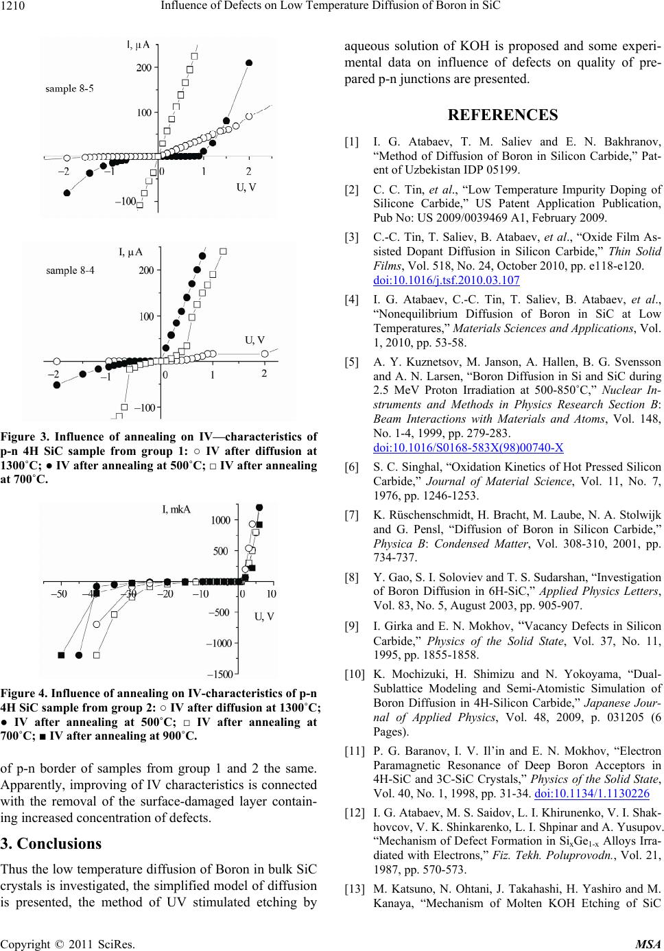 Influence of Defects on Low Temperature Diffusion of Boron in SiC 1210 Figure 3. Influence of annealing on IV—characteristics of p-n 4H SiC sample from group 1: ○ IV after diffusion at 1300˚C; ● IV after annealing at 500˚C; □ IV after annealing at 700˚C. Figure 4. Influence of annealing on IV-characteristics of p-n 4H SiC sample from group 2: ○ IV after diffusion at 1300˚C; ● IV after annealing at 500˚C; □ IV after annealing at 700˚C; ■ IV after annealing at 900˚C. of p-n border of samples from group 1 and 2 the same. Apparently, improving of IV characteristics is connected with the removal of the surface-damaged layer contain- ing increased conce nt rati o n o f de fects. 3. Conclusions Thus the low temperature diffusion of Boron in bulk SiC crystals is investigated, the simplified model of diffusion is presented, the method of UV stimulated etching by aqueous solution of KOH is proposed and some experi- mental data on influence of defects on quality of pre- pared p-n juncti ons are presen ted. REFERENCES [1] I. G. Atabaev, T. M. Saliev and E. N. Bakhranov, “Method of Diffusion of Boron in Silicon Carbide,” Pat- ent of Uzbekistan IDP 05199. [2] C. C. Tin, et al., “Low Temperature Impurity Doping of Silicone Carbide,” US Patent Application Publication, Pub No: US 2009/0039469 A1, February 2009. [3] C.-C. Tin, T. Saliev, B. Atabaev, et al., “Oxide Film As- sisted Dopant Diffusion in Silicon Carbide,” Thin Solid Films, Vol. 518, No. 24, October 2010, pp. e118-e120. doi:10.1016/j.tsf.2010.03.107 [4] I. G. Atabaev, C.-C. Tin, T. Saliev, B. Atabaev, et al., “Nonequilibrium Diffusion of Boron in SiC at Low Temperatures,” Materials Sciences and Applications, Vol. 1, 2010, pp. 53-58. [5] A. Y. Kuznetsov, M. Janson, A. Hallen, B. G. Svensson and A. N. Larsen, “Boron Diffusion in Si and SiC during 2.5 MeV Proton Irradiation at 500-850˚C,” Nuclear In- struments and Methods in Physics Research Section B: Beam Interactions with Materials and Atoms, Vol. 148, No. 1-4, 1999, pp. 279-283. doi:10.1016/S0168-583X(98)00740-X [6] S. C. Singhal, “Oxidation Kinetics of Hot Pressed Silicon Carbide,” Journal of Material Science, Vol. 11, No. 7, 1976, pp. 1246-1253. [7] K. Rüschenschmidt, H. Bracht, M. Laube, N. A. Stolwijk and G. Pensl, “Diffusion of Boron in Silicon Carbide,” Physica B: Condensed Matter, Vol. 308-310, 2001, pp. 734-737. [8] Y. Gao, S. I. Soloviev and T. S. Sudarshan, “Investigation of Boron Diffusion in 6H-SiC,” Applied Physics Letters, Vol. 83, No. 5, August 2003, pp. 905-907. [9] I. Girka and E. N. Mokhov, “Vacancy Defects in Silicon Carbide,” Physics of the Solid State, Vol. 37, No. 11, 1995, pp. 1855-1858. [10] K. Mochizuki, H. Shimizu and N. Yokoyama, “Dual- Sublattice Modeling and Semi-Atomistic Simulation of Boron Diffusion in 4H-Silicon Carbide,” Japanese Jour- nal of Applied Physics, Vol. 48, 2009, p. 031205 (6 Pages). [11] P. G. Baranov, I. V. Il’in and E. N. Mokhov, “Electron Paramagnetic Resonance of Deep Boron Acceptors in 4H-SiC and 3C-SiC Crystals,” Physics of the Solid State, Vol. 40, No. 1, 1998, pp. 31-34. doi:10.1134/1.1130226 [12] I. G. Atabaev, M. S. Saidov, L. I. Khirunenko, V. I. Shak- hovcov, V. K. Shinkarenko, L. I. Shpinar and A. Yusupov. “Mechanism of Defect Formation in SixGe1-x Alloys Irra- diated with Electrons,” Fiz. Tekh. Poluprovodn., Vol. 21, 1987, pp. 570-573. [13] M. Katsuno, N. Ohtani, J. Takahashi, H. Yashiro and M. Kanaya, “Mechanism of Molten KOH Etching of SiC Copyright © 2011 SciRes. MSA 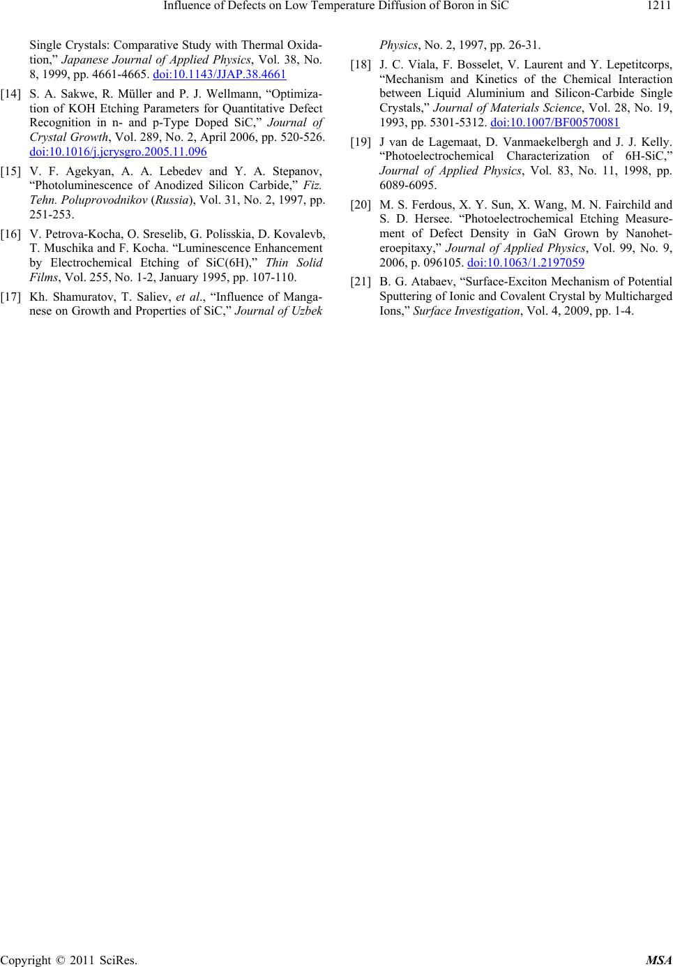 Influence of Defects on Low Temperature Diffusion of Boron in SiC Copyright © 2011 SciRes. MSA 1211 Single Crysta ls: Comparative Study wi th Thermal Oxida- tion,” Japanese Journal of Applied Physics, Vol. 38, No. 8, 1999, pp. 4661-4665. doi:10.1143/JJAP.38.4661 [14] S. A. Sakwe, R. Müller and P. J. Wellmann, “Optimiza- tion of KOH Etching Parameters for Quantitative Defect Recognition in n- and p-Type Doped SiC,” Journal of Crystal Growth, Vol. 289, No. 2, April 2006, pp. 520-526. doi:10.1016/j.jcrysgro.2005.11.096 [15] V. F. Agekyan, A. A. Lebedev and Y. A. Stepanov, “Photoluminescence of Anodized Silicon Carbide,” Fiz. Tehn. Poluprovodnikov (Russia), Vol. 31, No. 2, 1997, pp. 251-253. [16] V. Petrova-Kocha, O. Sreselib, G. Polisskia, D. Kovalevb, T. Muschika and F. Kocha. “Luminescence Enhancement by Electrochemical Etching of SiC(6H),” Thin Solid Films, Vol. 255, No. 1-2, January 1995, pp. 107-110. [17] Kh. Shamuratov, T. Saliev, et al., “Influence of Manga- nese on Growth and Properties of SiC,” Journal of Uzbek Physics, No. 2, 1997, pp. 26-31. [18] J. C. Viala, F. Bosselet, V. Laurent and Y. Lepetitcorps, “Mechanism and Kinetics of the Chemical Interaction between Liquid Aluminium and Silicon-Carbide Single Crystals,” Journal of Materials Science, Vol. 28, No. 19, 1993, pp. 5301-5312. doi:10.1007/BF00570081 [19] J van de Lagemaat, D. Vanmaekelbergh and J. J. Kelly. “Photoelectrochemical Characterization of 6H-SiC,” Journal of Applied Physics, Vol. 83, No. 11, 1998, pp. 6089-6095. [20] M. S. Ferdous, X. Y. Sun, X. Wang, M. N. Fairchild and S. D. Hersee. “Photoelectrochemical Etching Measure- ment of Defect Density in GaN Grown by Nanohet- eroepitaxy,” Journal of Applied Physics, Vol. 99, No. 9, 2006, p. 096105. doi:10.1063/1.2197059 [21] B. G. Atabaev, “Surface-Exciton Mechanism of Potential Sputtering of Ionic and Covalent Crystal by Multicharged Ions,” Surface Investigation, Vol. 4, 2009, pp. 1-4.
|