Paper Menu >>
Journal Menu >>
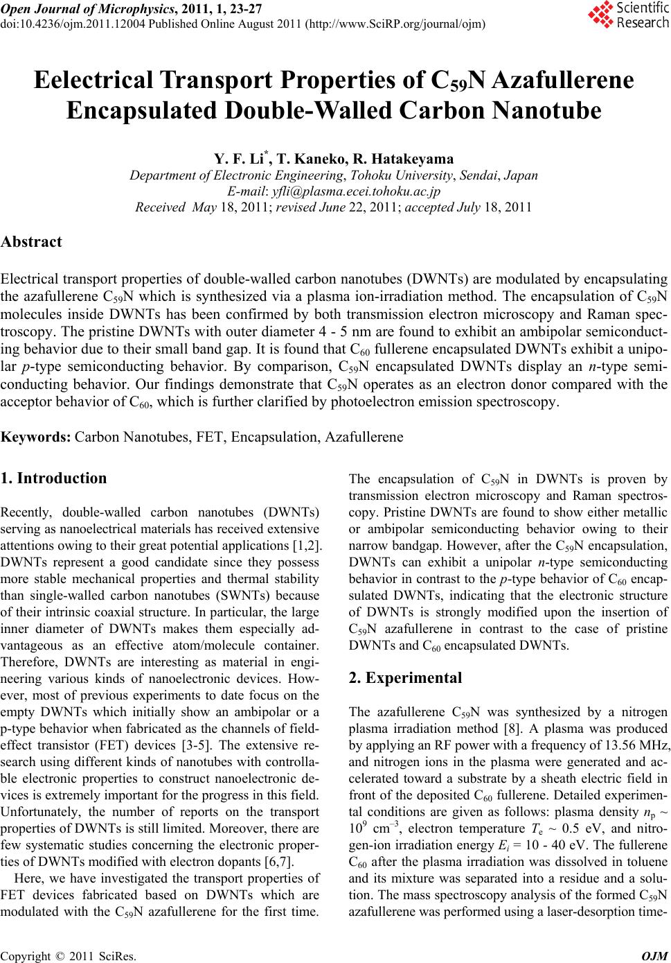 Open Journal of Microphysics, 2011, 1, 23-27 doi:10.4236/ojm.2011.12004 Published Online August 2011 (http://www.SciRP.org/journal/ojm) Copyright © 2011 SciRes. OJM Eelectrical Transport Properties of C59N Azafullerene Encapsulated Double-Walled Carbon Nanotube Y. F. Li*, T. Kaneko, R. Hatakeyama Department of Electronic Engineering, Tohoku University, Sendai, Japan E-mail: yfli@plasma.ecei.tohoku.ac.jp Received May 18, 2011; revised June 22, 2011; accepted July 18, 2011 Abstract Electrical transport properties of double-walled carbon nanotubes (DWNTs) are modulated by encapsulating the azafullerene C59N which is synthesized via a plasma ion-irradiation method. The encapsulation of C59N molecules inside DWNTs has been confirmed by both transmission electron microscopy and Raman spec- troscopy. The pristine DWNTs with outer diameter 4 - 5 nm are found to exhibit an ambipolar semiconduct- ing behavior due to their small band gap. It is found that C60 fullerene encapsulated DWNTs exhibit a unipo- lar p-type semiconducting behavior. By comparison, C59N encapsulated DWNTs display an n-type semi- conducting behavior. Our findings demonstrate that C59N operates as an electron donor compared with the acceptor behavior of C60, which is further clarified by photoelectron emission spectroscopy. Keywords: Carbon Nanotubes, FET, Encapsulation, Azafullerene 1. Introduction Recently, double-walled carbon nanotubes (DWNTs) serving as nanoelectrical materials has received extensive attentions owing to their great potential applications [1,2]. DWNTs represent a good candidate since they possess more stable mechanical properties and thermal stability than single-walled carbon nanotubes (SWNTs) because of their intrinsic coaxial structure. In particular, the large inner diameter of DWNTs makes them especially ad- vantageous as an effective atom/molecule container. Therefore, DWNTs are interesting as material in engi- neering various kinds of nanoelectronic devices. How- ever, most of previous experiments to date focus on the empty DWNTs which initially show an ambipolar or a p-type behavior when fabricated as the channels of field- effect transistor (FET) devices [3-5]. The extensive re- search using different kinds of nanotubes with controlla- ble electronic properties to construct nanoelectronic de- vices is extremely important for the progress in this field. Unfortunately, the number of reports on the transport properties of DWNTs is still limited. Moreover, there are few systematic studies concerning the electronic proper- ties of DWNTs modified with electron dopants [6,7]. Here, we have investigated the transport properties of FET devices fabricated based on DWNTs which are modulated with the C59N azafullerene for the first time. The encapsulation of C59N in DWNTs is proven by transmission electron microscopy and Raman spectros- copy. Pristine DWNTs are found to show either metallic or ambipolar semiconducting behavior owing to their narrow bandgap. However, after the C59N encapsulation, DWNTs can exhibit a unipolar n-type semiconducting behavior in contrast to the p-type behavior of C60 encap- sulated DWNTs, indicating that the electronic structure of DWNTs is strongly modified upon the insertion of C59N azafullerene in contrast to the case of pristine DWNTs and C60 encapsulated DWNTs. 2. Experimental The azafullerene C59N was synthesized by a nitrogen plasma irradiation method [8]. A plasma was produced by applying an RF power with a frequency of 13.56 MHz, and nitrogen ions in the plasma were generated and ac- celerated toward a substrate by a sheath electric field in front of the deposited C60 fullerene. Detailed experimen- tal conditions are given as follows: plasma density np ~ 109 cm–3, electron temperature Te ~ 0.5 eV, and nitro- gen-ion irradiation energy Ei = 10 - 40 eV. The fullerene C60 after the plasma irradiation was dissolved in toluene and its mixture was separated into a residue and a solu- tion. The mass spectroscopy analysis of the formed C59N azafullerene was performed using a laser-desorption time- 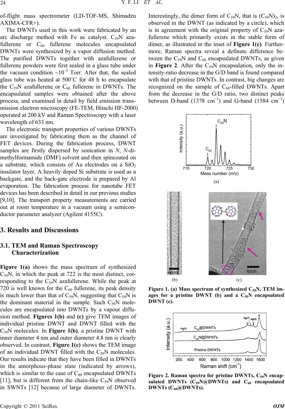 24 Y. F. LI ET AL. of-flight mass spectrometer (LD-TOF-MS, Shimadzu AXIMA-CFR+). The DWNTs used in this work were fabricated by an arc discharge method with Fe as catalyst. C59N aza- fullerene or C60 fullerene molecules encapsulated DWNTs were synthesized by a vapor diffusion method. The purified DWNTs together with azafullerene or fullerene powders were first sealed in a glass tube under the vacuum condition ~10–5 Torr. After that, the sealed glass tube was heated at 500˚C for 48 h to encapsulate the C59N azafullerene or C60 fullerene in DWNTs. The encapsulated samples were obtained after the above process, and examined in detail by field emission trans- mission electron microscopy (FE-TEM, Hitachi HF-2000) operated at 200 kV and Raman Spectroscopy with a laser wavelength of 633 nm. The electronic transport properties of various DWNTs are investigated by fabricating them as the channel of FET devices. During the fabrication process, DWNT samples are firstly dispersed by sonication in N, N-di- methylformamide (DMF) solvent and then spincoated on a substrate, which consists of Au electrodes on a SiO2 insulator layer. A heavily doped Si substrate is used as a backgate, and the back-gate electrode is prepared by Al evaporation. The fabrication process for nanotube FET devices has been described in detail in our previous studies [9,10]. The transport property measurements are carried out at room temperature in a vacuum using a semicon- ductor parameter analyzer (Agilent 4155C). 3. Results and Discussions 3.1. TEM and Raman Spectroscopy Characterization Figure 1(a) shows the mass spectrum of synthesized C59N, in which the peak at 722 is the most distinct, cor- responding to the C59N azafullerene. While the peak at 720 is well known for the C60 fullerene, its peak density is much lower than that of C59N, suggesting that C59N is the dominant material in the sample. Such C59N mole- cules are encapsulated into DWNTs by a vapour diffu- sion method. Figures 1(b) and (c) give TEM images of individual pristine DWNT and DWNT filled with the C59N molecules. In Figure 1(b), a pristine DWNT with inner diameter 4 nm and outer diameter 4.8 nm is clearly observed. In contrast, Figure 1(c) shows the TEM image of an individual DWNT filled with the C59N molecules. Our results indicate that they have been filled in DWNTs in the amorphous-phase state (indicated by arrows), which is similar to the case of C60 encapsulated DWNTs [11], but is different from the chain-like C59N observed in SWNTs [12] because of large diameter of DWNTs. Interestingly, the dimer form of C59N, that is (C59N)2, is observed in the DWNT (as indicated by a circle), which is in agreement with the original property of C59N aza- fullerene which primarily exists in the stable form of dimer, as illustrated in the inset of Figure 1(c). Further- more, Raman spectra reveal a definate difference be- tween the C59N and C60 encapsulated DWNTs, as given in Figure 2. After the C59N encapsulation, only the in- tensity-ratio decrease in the G/D band is found compared with that of pristine DWNTs. In contrast, big changes are recognized on the sample of C60-filled DWNTs. Apart from the decrease in the G/D ratio, two distinct peaks between D-band (1378 cm–1) and G-band (1584 cm–1) 715 720725 73 0 Intensity (a.u.) C60 C59N Mass number (m/z) (a) (a) (b) (c) Figure 1. (a) Mass spectrum of synthesized C59N, TEM im- ages for a pristine DWNT (b) and a C59N encapsulated DWNT (c). Figure 2. Raman spectra for pristine DWNTs, C59N encap- sulated DWNTs (C59N@DWNTs) and C60 encapsulated DWNTs (C60@DWNTs). Copyright © 2011 SciRes. OJM  Y. F. LI ET AL. 25 are observed. One strong peak at 1476 cm–1 corresponds to the intermolecular Raman active frequency (tangential mode) Ag (2) of C60 molecules, and the other weak peak at 1437 cm–1 near the D-band can be attributed to the Hg (7) mode of C60 molecules. A very weak peak for the Ag (2) mode observed in C59N encapsulated DWNTs com- pared with that observed for C60 encapsulated DWNTs may possibly be explained in terms of their different electronic structure. 3.2. Transport Properties of C59N Encapsulated DWNTs The electrical transports properties of DWNTs are meas- ured based on an FET configuration, as schematically illustrated in the inset of Figure 3. Our measurements demonstrate that the transport properties of pristine semiconducting DWNTs show an ambipolar behavior, as shown in Figure 3. The characteristics of source-drain current versus gate voltage (IDS-VG) curves indicate that the device conducts either electrons or holes depending on the gate bias when different source-drain voltages (VDS) from 0 to 1 V are applied. The region on the left-hand for VG –20 V corresponds to the p-type con- duction and the n-type conductance is observed in the right-hand region for VG –20 V. The current-voltage characteristics of the device indicate that the source-drain current increases strongly with increasing the negative gate voltage in the p-channel and increasing the positive gate voltage in the n-channel, respectively. Particularly, the observed saturated conductance in the p-channel typically appears to be two or three times larger than that observed in the n-channel for pristine DWNT-FETs. In contrast, unipolar n-type DWNT-FETs can be obtained by the C59N-encapsulation, as shown in Figure 4(a), where the characteristics of IDS-VG measured at different VDS ranging from 0 to 0.1 V in steps of 0.02 V indicate clearly that the FET device exhibits an excellent n-type semiconducting behavior, and no amibipolar behavior is found due to the strong electron-donating property of C59N. The threshold voltage (Vth) necessary to com- pletely deplete the nanotubes is about –20 V at VDS = 0.1 V, which is similar to the value of Vth for the n-type re- gion in the pristine ambipolar DWNTs. To further esti- mate the performance of the n-type FET device, the IDS-VDS curves are measured with VDS ranging from –0.1 to 0.1 V by applying different gate voltages from –30 V to 20 V, as shown in Figure 4(b). The conductance of device is significantly suppressed by decreasing the gate voltages from 20 V until the gate voltage reaches about –40 V, which also exhibits a reproducible characteristic for the n-type nanotube FETs, being consistent with the result in Figure 4(a). The above result demonstrates -40 -2002040 0 400 800 1200 IDS (nA) VG(V) VDS =0 V VDS =0.2 V VDS =0.4 V VDS =0.6 V VDS =0.8 V VDS =1.0 V Figure 3. (a) Drain-source current versus gate voltage (IDS-VG) characteristics for an amibipolar semiconducting DWNT-FET measured with bias voltage (VDS) ranging from 0 to 1 V in steps of 0.2 V. The inset shows the FET configu- ration. evidently that there is the strong electron transfer from C59N to the encapsulated DWNT; as a result, the electron density of conduction band of DWNT is strongly modi- fied. In contrast, for the C60-encapsulation, the transport characteristic is completely opposite to that observed for the C59N encapsulated DWNTs, and the unipolar p-type semiconducting DWNTs are obtained, as given in Fig- ures 4(c) and (d). The IDS-VG characteristics demonstrate that no n-type conductance is found during the meas- urements performed with VDS in the range of –1 ~ 1 V. The observed Vth near –10 V at VDS = 1 V shows a clear upshift compared with that (–20 V) observed for the p-type region of pristine DWNTs. In addition, the IDS-VDS curve characteristics in Figure 4(d) indicate that the conductance of the FET device is reduced by increasing the gate voltage from –40 to 40 V, which is opposite to that observed in Figure 4(b) for the device based on the C59N encapsulated DWNT. The present experiments suggest that the C59N molecules exert a strong elec- tron-donating effect on DWNTs compared with the elec- tron-accepting behavior of C60. In order to analyze electronic structures of C59N and C60, their work functions are investigated by ultraviolet photoemission spectroscopy (UPS), which can provide a mechanical insight into the charge transfer process be- tween the encapsulated azafullerene and DWNTs. Fig- ure 5 presents the photoelectron emission spectra of C60 and C59N, in which the work function of C59N is deter- mined to be about 5.5 eV, much smaller than that (6.1 eV) observed for C60, suggesting evidently that the electronic property of C59N is significantly different from that of C60. Namely, the nitrogen-atom bonding with C atom makes the release of electrons easier in the case of C59N azafullerene. Therefore, by combining the electrical transport properties of FETs and photoelectron emission spectra, the n-type semiconducting behavior of DWNTs Copyright © 2011 SciRes. OJM 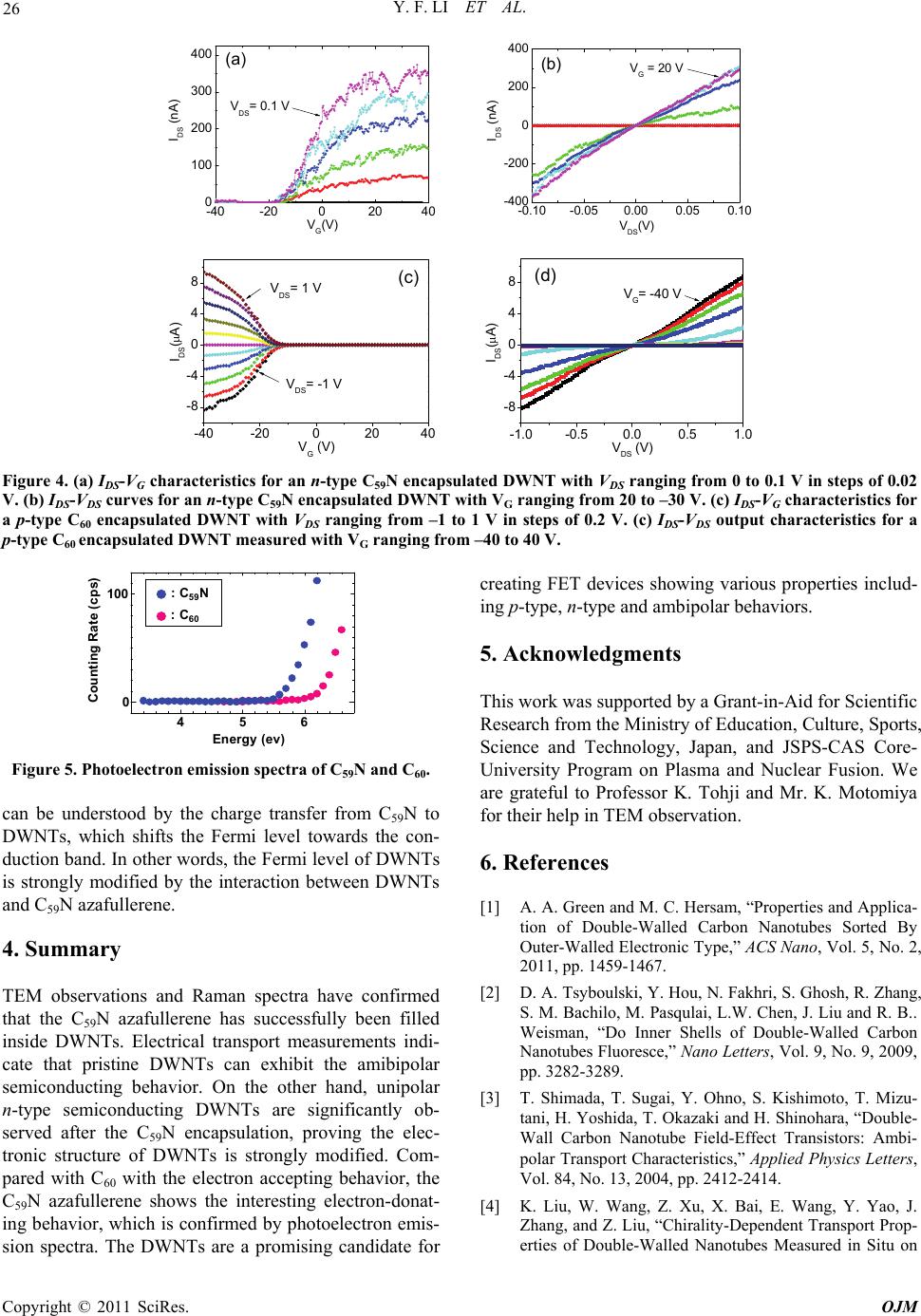 Y. F. LI ET AL. Copyright © 2011 SciRes. OJM 26 -40 -2002040 0 100 200 300 400 IDS (nA) VG(V) VDS= 0.1 V (a) -0.10 -0.050.000.050.10 -400 -200 0 200 400 VG = 20 V VDS(V) IDS (nA) (b) -40 -2002040 -8 -4 0 4 8 VDS= -1 V IDS(A) VG (V) (c) VDS= 1 V -1.0 -0.50.00.51.0 -8 -4 0 4 8 IDS(A) VDS (V) (d) VG= -40 V Figure 4. (a) IDS-VG characteristics for an n-type C59N encapsulated DWNT with VDS ranging from 0 to 0.1 V in steps of 0.02 V. (b) IDS-VDS curves for an n-type C59N encapsulated DWNT with VG ranging from 20 to –30 V. (c) IDS-VG characteristics for a p-type C60 encapsulated DWNT with VDS ranging from –1 to 1 V in steps of 0.2 V. (c) IDS-VDS output characteristics for a p-type C60 encapsulated DWNT measured with VG ranging from –40 to 40 V. 456 0 100 Energy (ev) Counting Rate (cps) : C59N : C60 Figure 5. Photoelectron emission spectra of C59N and C60. can be understood by the charge transfer from C59N to DWNTs, which shifts the Fermi level towards the con- duction band. In other words, the Fermi level of DWNTs is strongly modified by the interaction between DWNTs and C59N azafullerene. 4. Summary TEM observations and Raman spectra have confirmed that the C59N azafullerene has successfully been filled inside DWNTs. Electrical transport measurements indi- cate that pristine DWNTs can exhibit the amibipolar semiconducting behavior. On the other hand, unipolar n-type semiconducting DWNTs are significantly ob- served after the C59N encapsulation, proving the elec- tronic structure of DWNTs is strongly modified. Com- pared with C60 with the electron accepting behavior, the C59N azafullerene shows the interesting electron-donat- ing behavior, which is confirmed by photoelectron emis- sion spectra. The DWNTs are a promising candidate for creating FET devices showing various properties includ- ing p-type, n-type and ambipolar behaviors. 5. Acknowledgments This work was supported by a Grant-in-Aid for Scientific Research from the Ministry of Education, Culture, Sports, Science and Technology, Japan, and JSPS-CAS Core- University Program on Plasma and Nuclear Fusion. We are grateful to Professor K. Tohji and Mr. K. Motomiya for their help in TEM observation. 6. References [1] A. A. Green and M. C. Hersam, “Properties and Applica- tion of Double-Walled Carbon Nanotubes Sorted By Outer-Walled Electronic Type,” ACS Nano, Vol. 5, No. 2, 2011, pp. 1459-1467. [2] D. A. Tsyboulski, Y. Hou, N. Fakhri, S. Ghosh, R. Zhang, S. M. Bachilo, M. Pasqulai, L.W. Chen, J. Liu and R. B.. Weisman, “Do Inner Shells of Double-Walled Carbon Nanotubes Fluoresce,” Nano Letters, Vol. 9, No. 9, 2009, pp. 3282-3289. [3] T. Shimada, T. Sugai, Y. Ohno, S. Kishimoto, T. Mizu- tani, H. Yoshida, T. Okazaki and H. Shinohara, “Double- Wall Carbon Nanotube Field-Effect Transistors: Ambi- polar Transport Characteristics,” Applied Physics Letters, Vol. 84, No. 13, 2004, pp. 2412-2414. [4] K. Liu, W. Wang, Z. Xu, X. Bai, E. Wang, Y. Yao, J. Zhang, and Z. Liu, “Chirality-Dependent Transport Prop- erties of Double-Walled Nanotubes Measured in Situ on 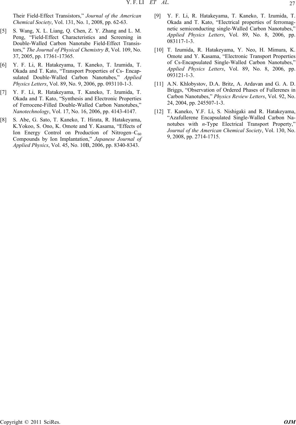 Y. F. LI ET AL. 27 Their Field-Effect Transistors,” Journal of the American Chemical Society, Vol. 131, No. 1, 2008, pp. 62-63. [5] S. Wang, X. L. Liang, Q. Chen, Z. Y. Zhang and L. M. Peng, “Field-Effect Characteristics and Screening in Double-Walled Carbon Nanotube Field-Effect Transis- tors,” The Journal of Physical Chemistry B, Vol. 109, No. 37, 2005, pp. 17361-17365. [6] Y. F. Li, R. Hatakeyama, T. Kaneko, T. Izumida, T. Okada and T. Kato, “Transport Properties of Cs- Encap- sulated Double-Walled Carbon Nanotubes,” Applied Physics Letters, Vol. 89, No. 9, 2006, pp. 093110-1-3. [7] Y. F. Li, R. Hatakeyama, T. Kaneko, T. Izumida, T. Okada and T. Kato, “Synthesis and Electronic Properties of Ferrocene-Filled Double-Walled Carbon Nanotubes,” Nanotechnology, Vol. 17, No. 16, 2006, pp. 4143-4147. [8] S. Abe, G. Sato, T. Kaneko, T. Hirata, R. Hatakeyama, K.Yokoo, S. Ono, K. Omote and Y. Kasama, “Effects of Ion Energy Control on Production of Nitrogen–C60 Compounds by Ion Implantation,” Japanese Journal of Applied Physics, Vol. 45, No. 10B, 2006, pp. 8340-8343. [9] Y. F. Li, R. Hatakeyama, T. Kaneko, T. Izumida, T. Okada and T. Kato, “Electrical properties of ferromag- netic semiconducting single-Walled Carbon Nanotubes,” Applied Physics Letters, Vol. 89, No. 8, 2006, pp. 083117-1-3. [10] T. Izumida, R. Hatakeyama, Y. Neo, H. Mimura, K. Omote and Y. Kasama, “Electronic Transport Properties of Cs-Encapsulated Single-Walled Carbon Nanotubes,” Applied Physics Letters, Vol. 89, No. 8, 2006, pp. 093121-1-3. [11] A.N. Khlobystov, D.A. Britz, A. Ardavan and G. A. D. Briggs, “Observation of Ordered Phases of Fullerenes in Carbon Nanotubes,” Physics Review Letters, Vol. 92, No. 24, 2004, pp. 245507-1-3. [12] T. Kaneko, Y.F. Li, S. Nishigaki and R. Hatakeyama, “Azafullerene Encapsulated Single-Walled Carbon Na- notubes with n-Type Electrical Transport Property,” Journal of the American Chemical Society, Vol. 130, No. 9, 2008, pp. 2714-1715. Copyright © 2011 SciRes. OJM |