Journal of Electromagnetic Analysis and Applications
Vol. 3 No. 7 (2011) , Article ID: 5911 , 6 pages DOI:10.4236/jemaa.2011.37047
Low Noise Amplifier Design for Digital Television Applications
![]()
1School of Electrical and Computer Engineering, National Technological University of Athens, Athens, Greece; 2Hellenic Naval Academy, Piraeus, Greece.
Email: atsarakl@mail.ntua.gr, evka@hna.gr
Received May 4th, 2011; revised June 2nd, 2011; accepted June 12th, 2011.
Keywords: Digital television, Low Noise Amplifiers, Microwave Circuits
ABSTRACT
The DVB-T (Digital Video Broadcasting—Terrestrial) standard is being deployed in many parts of the world for digital broadcasting services, providing a variety of features extending the capabilities of the older analog ones. In this paper, a two-stage low noise amplifier (LNA) is designed for use with the DVB-T standard. The design is employed based on microstrip. The microwave design meets all the specifications required, achieving input and output return loss below −10 dB, high gain of 35 dB and high linearity. Low noise figure of 1.3 dB is achieved with the use of pHEMT transistor technology.
1. Introduction
Digital television broadcasting standards are planned to replace the current analog ones in most parts of the world. For Europe, this standard is DVB-T (Digital Video Broadcasting—Terrestrial) which includes a variety of features not only in the physical layer but also in the binary stream structure [1], which leads to a reduction of the spectrum needed, better radio coverage, improved image quality and interactive services capability. DVB-T is designed to operate in the IV and V bands corresponding to the analog television bands, so that the users do not change their antennas and the favorable UHF propagation characteristics are maintained. Specifically, the whole frequency band used by DVB-T is 470 - 862 MHz, however the band is not intended to be fully used. The frequency band 790 - 862 MHz, called Digital Dividend, is intended to be used for mobile applications or for special digital television services [2]. Therefore, several countries practically do not take into account this band for the deployment of the digital television broadcasting scheme, using only the UHF frequency band 470 - 790 MHz, which corresponds to channels 21 - 60 of the analog channel allocation, while the channels 61 - 69, are committed for Digital Dividend applications.
Low noise amplifiers are used at receiver’s side in all communications systems in order to offer the first amplification to the received signal with the addition of the minimum noise [3]. Although LNAs are parts of the receivers only, their design should take into account the general features of the whole communications system. Also, as part of the receiving chain the LNA is connected with the other parts of the receiver, a fact which imposes further limitations to the LNA.
The operation of the LNA in UHF television frequentcies means that microwave design should be applied. The design is based on microstrip, so limitations are posed. An appropriate transistor is selected and the bias circuit is designed afterwards. A one-stage amplifier is designed followed by the final two-stage amplifier design. The specifications defined for the application are met successfully.
2. LNA Specifications and Design Process
2.1. LNA Specifications
The specifications of the low noise amplifier are given in Table 1 [4]. The band in which the device will operate is the most commonly allocated DVB-T band of 470 - 790 MHz. Thus, the central frequency is 630 MHz. The gain of the low noise amplifier should be high and be combined with the gain of the other following components. In order to achieve high linearity, 1 dB compression point is chosen to be rather high. Noise figure should be lower
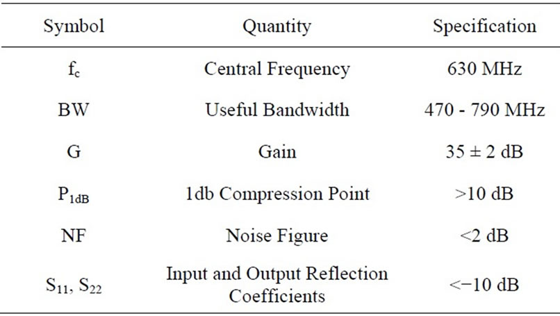
Table 1. LNA specifications.
than 2 dB, which is a rather strict requirement, but in modern devices, even lower noise figures can be achieved [5]. The input and output reflection coefficients typically are chosen to be lower than −10 dB in all useful bandwidth, in order to avoid harmful reflections.
Based on these specifications, a suitable transistor is chosen. MGA-53543 [6] meets all the requirements, with 17.4 dB gain at 0.9 GHz, and noise figure 1.5 dB. Its linearity exceeds the specifications and it needs +5 V bias. These characteristics are achieved due to pHEMT technology, especially the very low noise figure. Several designs with pHEMT can be found [7,8], especially for higher frequencies.
In order to meet the gain requirements, a two-staged amplifier is needed. As for the noise figure requirement, the first stage mainly determines its value, as it is known from microwave theory [9], so, as the stages will be identical, the noise figure will be almost 1.5 dB.
2.2. Substrate Characteristics
The substrate R04350 characteristics are given in Table 2. The input and output impedance should be 75 Ω for television applications. Thus, the width of the microstrip should be 0.77 mm, whereas the effective relative permittivity is 2.572.
2.3. Design Process
The low noise amplifier is designed with the use of Agilent’s Advanced Design System [10]. Transistor Sparameter model is used, along with the microstrip library components [11]. The design is optimized through random and gradient techniques, in order to achieve specified goals of input and output VSWRs (Voltage Standing Wave Ratio), used instead of reflection coefficient measure. Also, the tuning operation is used in order to optimize a single variable or a pair of variables but not the whole multi parametric design.
3. Bias Circuit
One of the most important design processes during an
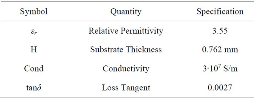
Table 2. Substrate characteristics.
amplifier design process is the bias circuit design, which is designed separately. The bias circuit, apart from providing the desired voltage level, deters power losses towards the supply.
Thus, the reflection coefficient of the bias circuit, as seen from the rest system, should be near 1 with zero phase. This means that the bias circuit should be seen as an open circuit from the rest system. As it is known from microwave theory, in order to achieve this, a short circuit in λg/4 distance, where λg is the microstrip wavelength, is required. Alternatively, a λg/4 open-circuited stub must be placed in λg/4 distance from the connection point with the rest circuit. The designed bias circuit is given in Figure 1.
In Figure 2 the reflection coefficient of the bias circuit is given. As it is expected, S11 is near open-circuit at the center frequency, although there is a small deviation at the edge frequencies. For better accuracy, the tuning capability of ADS was used instead of using directly λg/4 lengths and these lengths were estimated 74.2 mm. The two capacitances are used for isolation purposes.
4. Low Noise Amplifier Design
The amplifier should be two-staged in order to achieve gain requirements [4]. The full low noise amplifier design is shown in Figure 3.
Before simulating the whole design, the one stage amplifier was primarily simulated. It succeeded in all requirements therefore the two-stage amplifier could be designed. The two stages are identical, so the 17 dB gain of the one-stage amplifier is expected to double in the whole design. The design was optimized through random and gradient techniques, in order to meet the requirements of input and output VSWRs. All the parameters to be estimated were defined as variables and were optimized. The amplifier stages are placed after a DC block capacitor.
The width of all Microstop Lines, MLIN is 770 μm and the length is varying between 1 to 84 mm depending on the topology. So, the whole area is approximately 120 cm2. The distance from near edge of strip to first sidewall is more than 2.5 × 1028 mm. Other parameters are given in Table 2.
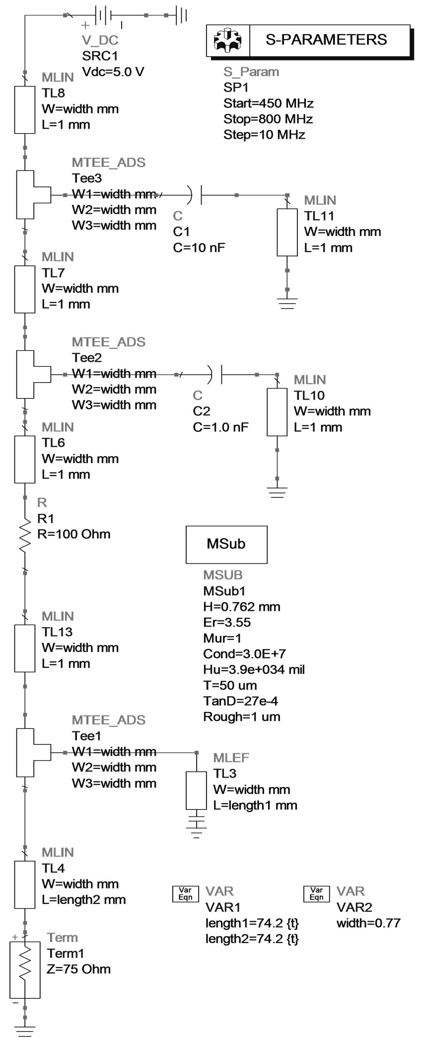
Figure 1. Designed bias circuit.
Ιn Figures 4 and 5, S11 and S22 are given. As it can be seen the reflection coefficients are below −10 dB for almost all the desirable frequency range despite the transistor not already being matched for 75 Ω, but for 50 Ω.
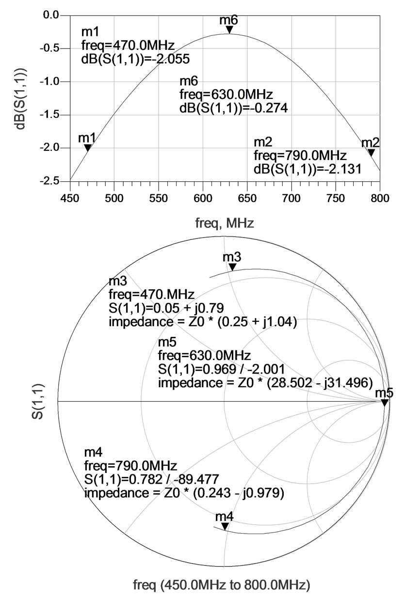
Figure 2. Bias circuit reflection coefficient.
The forward gain, shown in Figure 6, satisfies almost perfectly the specification of 35 ± 2 dB. Noise figure, given in Figure 7, is near 1.3 dB which is within specifications. Finally, the stability factor K is given in Figure 8 for the whole operation bandwidth of the transistor. The amplifier is unconditionally stable, as K > 1. Consequently, all the specifications are achieved.
Finally, in Figure 9 the main part of the layout without the bias branches is depicted. The transistor is provided in SOT343 packaging. The construction area is 16 × 8 cm and the majority of this area derives from the need for long microstrip lengths for the bias circuit.
The proposed solution satisfies both the noise and linearity requirements with moderate power consumption. Corporations such as MACOM, Avaco, Hittite provide CATV amplifiers, GaAs MMIC which exhibits low distortion in a lead-free miniature surface mount plastic package [12-14]. The novelty of this design lies in the achievement of low noise figure (NF) and high reverse isolation level across a wide bandwidth despite the resistive feedback topology. Moreover, employs a monolithic two stage design featuring a convenient 75 Ω input/output impedance.
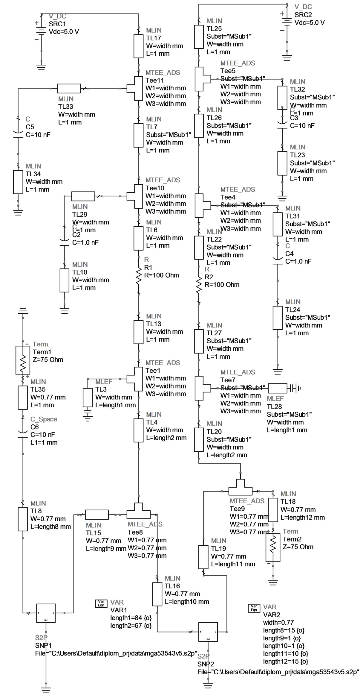
Figure 3. Whole two-stage amplifier design.
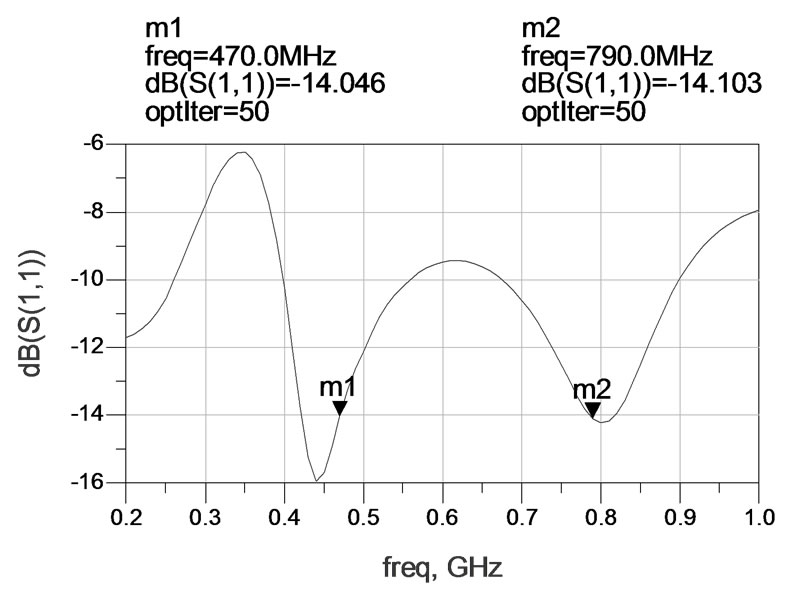
Figure 4. Input reflection coefficient.
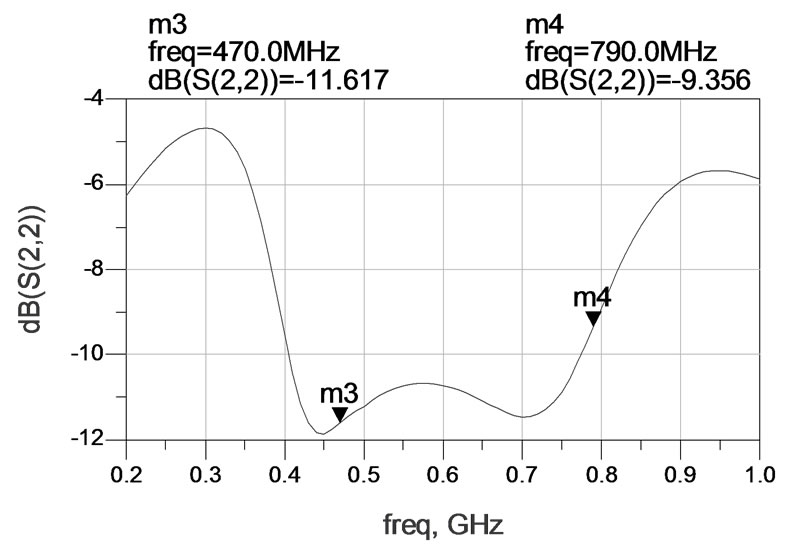
Figure 5. Output reflection coefficient.
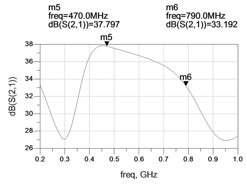
Figure 6. Forward gain.
5. Conclusions
A high performance highly integrated sub-GHz wide band two stage low-noise amplifier (LNA) for DVB-T applications is designed. A noise-canceling topology using a feed-forward current reuse common-source stage is presented to obtain low noise characteristics and high
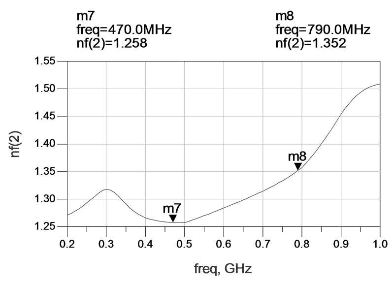
Figure 7. Noise figure.
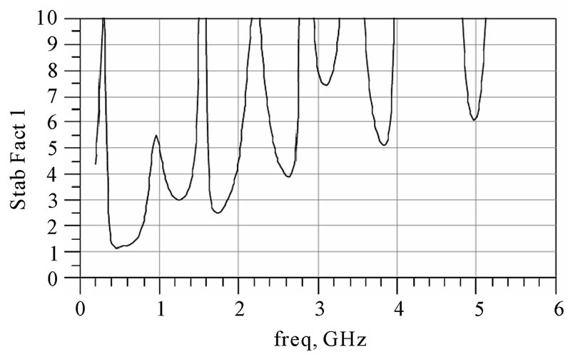
Figure 8. LNA stability factor.
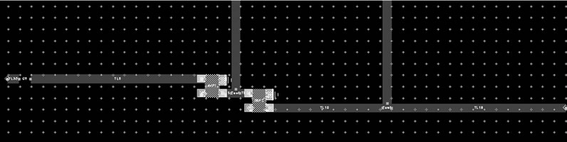
Figure 9. Main part of layout for construction purposes.
gain while achieving good wideband input matching within 470 - 790 MHz. In addition, linearization methods are appropriately utilized to improve the linearity.
The final LNA achieves a power gain of more than 33.4 dB, a minimum noise figure of 1.3 dB. The design follows all the modern design trends which include increased gain, minimized noise figure and microstrip design, even for UHF frequencies. The requirements are met with the use of pHEMT transistor technology, which allows for low noise and high gain. Optimization and tuning functions are used for achieving the specifications.
REFERENCES
- Joint Technical Committee, “Digital Video Broadcasting (DVB): Framing Structure, Channel, Coding and Modulation for Digital Terrestrial Television (DVB-T),” ETSI EN 300 744 v 1.2.1, January 1999.
- International Telecommunication Union, “Final Acts of the Regional Radiocommunication Conference for Planning of the Digital Terrestrial Broadcasting Service in Parts of Regions 1 and 3, in the Frequency Bands 174 - 230 MHz and 470 - 862 MHz (RRC-06),” Geneva, 2006.
- B. Razavi, “RF Microelectronics,” Prentice Hall, Upper Saddle River, 1997.
- A. Z. Tsaraklimanis “Low Noise Amplifier Design for Digital TV Applications,” MSc Dissertation Thesis, Univarsity of Athens, Athens, 2011. http://hippo.lib.uoa.gr/ipac20/ipac.jsp?sesion=B30866Q5P8421.5684&menu=search&aspect=subtab33&npp=30&ipp=20&spp=20&profile=maingr-tr&ri=&term=%CE%A4%CF%83%CE%B1%CF%81%CE%B1%CE%BA%CE%BB%CE%B7%CE%BC%CE%AC%CE%BD%CE%B7%CF%82&index=.GW&x=12&y=15&aspect=subtab33
- A. Youssef, A. Ismail and J. Haslett, “A Sub—2 dB Noise Figure Wideband LNA in 65 nm CMOS for Mobile TV Applications,” IEEE Radio and Wireless Symposium (RWS 2010), Santa Clara, 10 January 2010. doi:10.1109/RWS.2010.5434173
- AVAGO Technologies, “MGA-53543,” Datasheet, 2005.
- Y.-Y. Peng, K.-J. Lu and W.-Q. Sui, “A 7- to 14-Ghz GaAs pHEMT LNA with 1.1 dB Noise Figure and 26 dB Gain,” IEEE Microwave and Optical Letters, Vol. 52, No. 11, August 2010, pp. 2615-2617. doi:10.1002/mop.25547
- E. A. Karagianni and N. K. Uzunoglu, “A Monolithic GaAs FET Low Noise Amplifier Design for a Sub-SDH 51.84 Mb/sec,” The 7th International Conference on Advances in Communication and Control: Telecommunications/Signal Processing, Athens, 28 June-2 July 1999, pp. 555-563.
- G. Gonzalez, “Microwave Transistor Amplifier, Analysis and Design,” Prentice Hall, Englewood Cliffs, 1984.
- Agilent, “Advanced Design System (ADS), Overview,” 2010. http://www.home.agilent.com/agilent/product.jspx?cc=GR&lc=eng&ckey=1297113&nid=-34346.0.00&id=1297113
- E. A. Karagianni, Y. E. Stratakos, C. N. Vazouras and M. E. Fafalios, “Design and Fabrication of a Microstrip Hairpin-Line Filter by Appropriate Adaptation of Stripline Design Techniques,” 11th International Symposium on Microwave and Optical Technology, Monte Porzio Catone, 17-21 December 2007, pp. 509-512.
- AVAGO Technologies, “MGA-62563, Current-Adjustable, Low Noise Amplifier,” Data Sheet.
- Hittite, “HMC636ST89/636ST89E,” Data Sheet.
- Macom, “MAAMSS0060, Broadband CATV Amplifier 50-1000MHz,” Data Sheet.