Engineering
Vol. 2 No. 12 (2010) , Article ID: 3609 , 4 pages DOI:10.4236/eng.2010.212124
Texture ZnO Thin-Films and their Application as Front Electrode in Solar Cells
Department of Mechanical and Electronic Engineering, Jingdezhen Ceramics Institution, Jingdezhen, China
E-mail: 8489023@163.com
Conducting Oxide, Surface Of Micrograph, SnO2:F
Received September 20, 2010; revised October 26, 2010; accepted November 5, 2010
Keywords: Textured ZnO Thin-Film, Solar Cells Front Electrode, Magnetron Sputtering, Transparent
ABSTRACT
In this paper, three kinds of textured ZnO thin-films (the first kind has the textured structure with both columnar and polygon, the second posses pyramid-like textured structure only, and the third has the textured structure with both crater-like and pyramid-like), were prepared by three kinds of methods, and the application of these ZnO thin-films as a front electrode in solar cell was studied, respectively. In the first method with negative bias voltage and appropriate sputtering parameters, the textured structure with columnar and polygon on the surface of ZnO thin-film are both existence for the sample prepared by direct magnetron sputtering. Using as a front electrode in solar cell, the photoelectric conversion efficiency Eff of 7.00% was obtained. The second method is that by sputtering on the ZnO:Al self-supporting substrate, and the distribution of pyramid-like was gained. Moreover, the higher (8.25%) photoelectric conversion efficiency of solar cell was got. The last method is that by acid-etching the as-deposited ZnO thin-film which possesses mainly both columnar and polygon structure, and the textured ZnO thin-film with both crater-like and pyramid-like structure was obtained, and the photoelectric conversion efficiency of solar cell is 7.10% when using it as front electrode. These results show that the textured ZnO thin-film prepared on self-supporting substrate is more suitable for using as a front electrode in amorphous silicon cells.
1. Introduction
As a front electrode, the tin oxide doped with fluorine (SnO2:F) has been the most favored transparent conducting oxide (TCO) layer for hydrogenated amorphous silicon (a-Si:H) solar cells, due to its high temperature resistant substrates such as glass [1] or metal foils [2]. However, its electrical properties would be degraded seriously at a hydrogen plasma atmosphere [3]. Compared with SnO2:F, the textured aluminum doped zinc oxide (ZnO:Al) thin-film has the equivalent electrical properties, but also it has a lot of advantages, such as high electrical properties stability against hydrogen plasma, effective light trapping action, which is favorable to improve the a-Si:H solar cell performance as a front electrode, and it has attracted a great deal of attention [4-6]. At present there are two mature methods to prepare textured ZnO thin-films. The first one is acid-etching the as-deposited ZnO films, and the textured ZnO thin-film with crater-like structure could be obtained [7,8]. But it is difficult to be in master of the acid etching craft; and also, the textured ZnO thin-film with crater-like structure has poor performance in light trapping comparing to those with pyramid-like structure [9]. The second method is preparation of the textured ZnO thin-film with pyramid-like structure directly by MOCVD. However, the expensive equipment and high cost as well as bad thin-film density have limited its wide application [10]. In this paper, we attempt to prepare three kinds of textured ZnO thin-films by different methods. In order to compare the light trapping effect of these thin-films, the solar cells’ performance using three different kinds of ZnO thin-films as a front electrode are investigated, respectively.
2. Experimental
Three kinds of textured ZnO thin-film were prepared by different methods. The first method is to sputtering on the quartz substrate. In the experiments process, negative bias was added to increase the energy of particles, therefore, the probability of (100) and (101) surface growth which maybe relate to the pyramid-like textured ZnO thin-film, was increased. The sputtering parameters were as following: the working pressure was maintained at 1 Pa with ambient gas of Ar and O2 ratio of 30/3 and with the sputtering power of 150 W. The substrate temperature was set at 120ºC for 60min with -100V bias. This ZnO thin-film was labeled as sample A.
The second method is to sputtering ZnO on the as sol-gel prepared ZnO:Al self-supporting substrate. The precursor of sol-gel is Zn(CHCOO)2.2H2O, the ethylene glycol monomethyl ether and ethanol are used as solvent, and the ethanolamine is stabilizer. Zn(CHCOO)2.2H2O was dissolved in a mixed solvent of 2-methoxyethanol and ethanol, then monoethanolamine was added to the solution. After stirring, the transparent and uniform solution I was formed. In order to obtain the aluminium doped solution, Al(NO3)3·9H2O was dissolved in ethanol, and transparent solution II was obtained. The Solution II was added in solution I, at last the concentration of metal ions was 0.55 mol/L, and solution III was obtained. The wet film coated on the quartz substrates by sol-gel dip-coating method was dried at 150°C for 15 min immediately after coating. After repeating the coating procedure by eight times, the film was finally heated at 800°C for 60 min to form the ZnO:Al thin film, and the content of aluminium is 1% in the experiment. In the sputtering process, the working pressure was maintained at 1 Pa with Ar and O ratio of 30/3 ambient gases and the sputtering power was 200 W. The thin-film was prepared at 270°C deposition temperature of for 60 min.This sample was named as sample B.
The third method is to fabricate by acid-etching the as-deposited ZnO thin-film which prepared by sputtering. The experiments processes were as following. Firstly, the ZnO thin-film was fabricated by magnetron sputtering. In the sputtering process, the working pressure was maintained at 1 Pa with Ar and O ratio of 30/3 ambient gases and the sputtering power is 200 W. The substrate temperature was set at 27ºC for 60min with bias of -120V. The second process was acid-etched the as-deposited ZnO thin-film, and the experiment procedure were as following. (1) Hydrochloric acid solution of 0.5% was prepared. (2) The ZnO thin-film prepared by sputtering was acid-etched by immersing into the Hydrochloric acid solution for 30s. (3) Then the sample was taken out of the solution and by air or oven dry, and named as sample C.
For the magnetron sputtering, 99.999% high-purity Ar and 99.99% high-purity O2 were used as sputtering gas and reaction gas respectively. A sintered ceramic ZnO target with 90 mm in diameter and 5mm of thickness was employed. The quartz substrates were treated with traditional semiconductor clean technology, and the sputtering chamber was pumped down to below 4.2×10⁻⁴ Pa before each deposition.
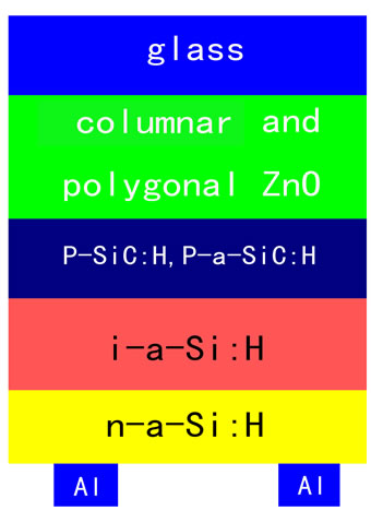
In order to compare the light trapping effect of samples A, B and C, the performance of a-Si:H solar cells using these films as the front electrode were measured, respectively. Three a-Si:H solar cells were deposited in an RF PECVD system. The structure of each solar cell was shown in Figure 1. The cell A with structure of glass/ZnO(sample A, 0.8 μm)/p-SiC:H, p-a-Si:H (~25 nm)/ i-a-Si:H (~0.5 μm)/n-a-Si:H (~30 nm)/Al; the cell B with structure of glass/ZnO:Al/ZnO (sample B, 1 μm)/p-SiC: H, p-a-Si:H (~25 nm)/i-a-Si:H (~0.5 μm)/n-a-Si:H (~30 nm)/ Al; the cell C with structure of glass/ZnO (sample C, 1 μm)/pc-Si:H (~90 nm)/p-SiC:H, p-a-Si:H (~25 nm)/ i-a-Si:H (~0.5 μm)/n-a-Si:H (~30 nm)/Al.
The resistivity of the samples was measured by four-probe method. An X-ray instrument (XRD-Rigaku D/ max2500) was used to characterize crystallization orientation of samples. SEM (SEM-JSM 6700F) was
 (a)
(a)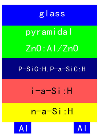 (b)
(b)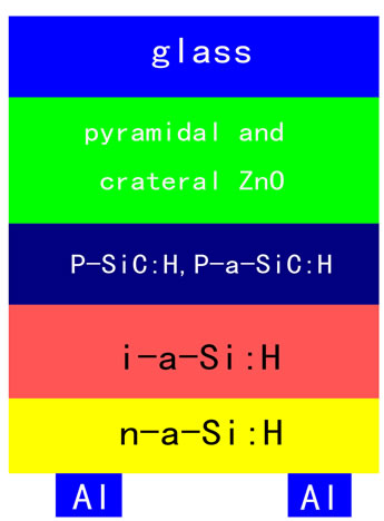 (c)
(c)
Figure 1. Schematic diagram of the solar cells. (a) Using the columnar and polygonal ZnO as a front electrode in solar cell; (b) using the pyramidal ZnO:Al/ZnO as a front electrode in solar cell; (c) using the pyramidal and cratered ZnO as a front electrode in solar cell.
used to observe surface morphology of films. The light-transmission of thin-film was identified by A UV2Vis-NIR Spectrophotometer (Backman-Du 8B Spectrophotometer) with wavelength in the range of 300~900 nm. All the sample measurements were performed at room temperature. The solar cell illuminated current-voltage characteristics were measured using a solar simulator (Wacom WXS-140S-Super) at standard test conditions (AM 1.5, 100 mW/cm2, 25ºC).
3. Results and Discussion
3.1. The Structure and Surface Morphology Characteristics of ZnO Films
Figure 2 and Figure 3 show the XRD and SEM results of ZnO films for the samples A~C, respectively. For the sample A, it can be seen that the peaks (100) and (101) appear besides the preferential (002) orientation peak (Figure 2(a)), and its SEM result also confirms that the columnar and polygon surface structure are both existence (Figure 3(a)). Figure 2(b) shows (002), (101), and the other peaks of ZnO crystals for the sample B. It was noticed that there was a different preferential (101) orientation, and its SEM result given in Figure 3(b) shows that the film has a textured pyramid-like structures, and the average grain size of the film is 0.8μm. For the sample C, the Figure 3(c) shows that the surface structures with pyramid-like and crater-like are mainly existence on the surface.
From the results on sample A and C, the ZnO thin-film prepared by sputtering with bias appears (100) and (101) preferred plane besides the (002) preferred plane. Zhi-Wei Yang et al. [11] reported that the molecules sputtering from ZnO target can obtain enough energy to crystallize due to arresting the positive ion to bomb substrate continuously by bias R. F. magnetron sputtering, as well as to increase deposition rate. Owing to the high deposition rate, it makes adatoms reduce oxidation due to the reduced exposure time in O2 atmosphere, and makes (002) preferred plane to be restricted which leads to appear parallel growth with polycrystal structure. Yue-Hui Hu et al. [10] reported that (101) and (100) orientations peaks, unless having a weak or a strong intensity, are related to the textured pyramid-like and polygon structure respectively. Figure 4 shows the relationship between microstructure and crystal growth orientation of ZnO films [10,12]. From Figure 4(a), it is obvious that the c-axis is growth perpendicular to the substrate for a columned structure for the ZnO film with preferential
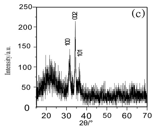
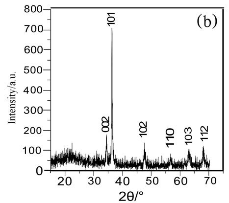
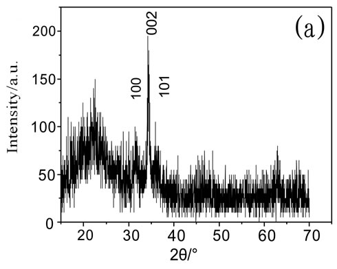
Figure 2. The XRD spectra of ZnO films. (a) The XRD spectrum of sample A; (b) the XRD spectrum of sample B; (c) the XRD spectrum of sample C.
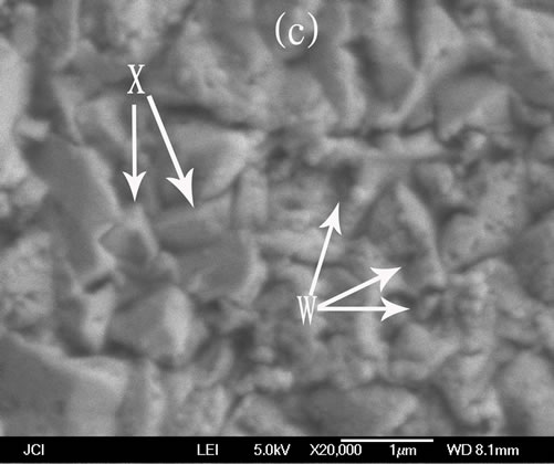
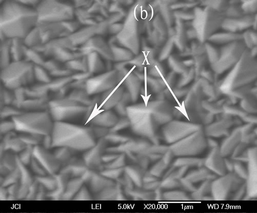
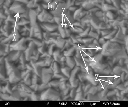
Figure 3. The SEM micrographs of ZnO films. (a) The SEM micrograph of sample A; (b) the SEM micrograph of sample B; (c) the SEM micrograph of sample C. In picture, X, Y, Z and W represented pyramid-like structure, polygon structure, columnar structure and crater-like structure, respectively.
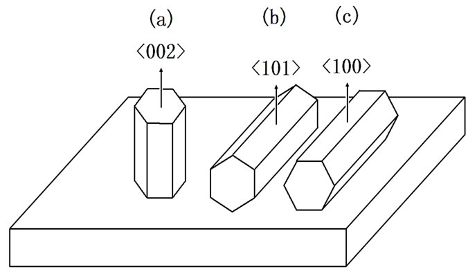
Figure 4. The relationship between microstructure and crystal growth orientation of ZnO films. (a) Correspond to that the c-axis is growth perpendicular to the substrate for a columned structure; (b) correspond to that the c-axis is growth parallel to the substrate for a pyramid-like structure; (c) correspond to that the c-axis is growth parallel to the substrate for a polygon structure.
(002) orientation. As shown in Figure 4(b), the c-axis is growth parallel to the substrate for a pyramid-like structure for the ZnO film with (101) crystal plane. Besides, the Figure 4(c) shows the c-axis is growth parallel to the substrate for a polygon structure for the ZnO film with (100) crystal plane. For the surface morphology of sample C with the structures both pyramid-like and crater-like mainly, the reason is that the surface morphology becomes crater-like by acid-etching the “table” of polygon, and the polygon structure reduces significantly.
3.2. Optical and Eelectrical Properties of ZnO Films
The transmittance spectra of samples are shown in Figure 5. The light-transmittance of the sample B is obviously lower than the others in the short wavelength range. Nonetheless, when the wavelength is larger than 560 nm, the light-transmittance for the sample B is above 80%. Moreover, light-transmittance of the sample C is slightly lower than the sample A in the short wavelength range.
Excluding the film thickness influence, these results mentioned above indicate that the light-trapping effect of thin-film is mainly determined by the pyramid-like textured structure. Consequently, the light-trapping effect of the sample B is best due to the surface morphology dominated by the pyramid-like structure (Figure 3(b)) [6]. While for the sample C, the surface morphology has both pyramid-like and crater-like structure (Figure 3(c)), and its light-trapping effect is second. In addition, for the sample A, its surface morphology are both columnar and polygon structure (Figure 3(a)), thus its light-trapping effect is worst. Figure 6 clarifies the light-trapping principle of pyramid-like structure. Taking vertical incidence of light as example, through multiple reflections and refractions of incident light intensity I0, the optical path increases in film, and the final reflex light intensity I4 is
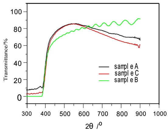
Figure 5. Optical transmission spectra of ZnO films.
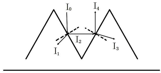
Figure 6. Light-trapping principle of pyramid-like morphology.
much less than the one that reflects directly by mirror structure at interfaces.
The electrical performance reveals that the resistivity of the sample B has the minimum value of 6.8×10⁻⁴ Ω.cm, while the sample C possesses the maximum value of 3.2×10⁻³ Ω.cm, and that of the sample A is about 8.4×10⁻⁴ Ω.cm. Owing to the higher crystalline qualities and larger grain sizes shown in Figures 3(a,b), samples A and B have a lower resistance. Figure 3(c) indicates a higher crystalline quality for sample C as well: even its resistance is the biggest. The possible reason is that the thin-film becomes thinner and the grain boundary area increases after acid-etching, as a result, the resistance increases.
3.3. Application of ZnO Film as a front Electrode in Amorphous Silicon Solar Cells
Using Samples A, B and C as front electrode, the amorphous silicon solar cells were fabricated and labeled as cell A, B and C, respectively. Figure 7 gives the I-V curves of cell A, B and C, and their electrical characteristics measured results are shown in Table 1. For the solar cell A, the short circuit current density Jsc, open voltage Voc, fill factor FF and conversion efficiency Eff are of 12.47 mA/cm2, 0.90 V, 0.631, 7.00%, respectively. For the solar cell B, the Jsc of 11.93 mA/cm2, Voc of 0.95 V, FF of 0.731 and Eff of 8.25% were obtained, respectively. For the solar cell C, the Jsc, Voc, FF and Eff are 11.81 mA/cm2, 0.91 V, 0.663 and 7.10%, respectively. It is
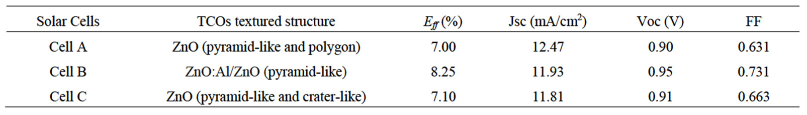
Table 1. Electrical characteristics of the solar cells using different textured structures as front electrode.
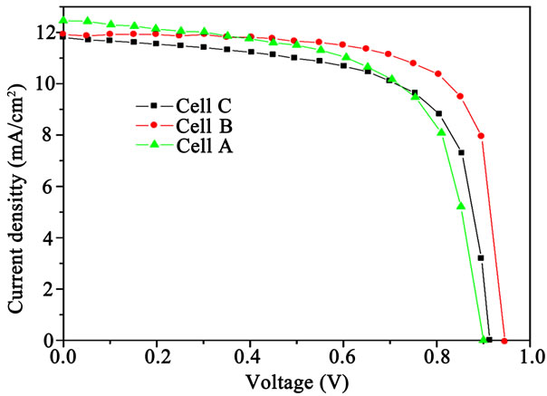
Figure 7. The I-V curves for solar cell A, B and C. For the solar cell A, the Jsc, Voc, FF and Eff are of 12.47 mA/cm2, 0.90 V, 0.631, 7.00%, respectively. For the solar cell B, the Jsc, Voc, FF and Eff are of 11.93 mA/cm2, 0.95 V, 0.731 and 8.25%, respectively. For the solar cell C, the Jsc, Voc, FF and Eff are 11.81 mA/cm2, 0.91 V, 0.663 and 7.10%, respectively.
shown that the performance of cell B is the best of all, and it is indicated that the textured ZnO thin-film with pyramid-like structure prepared on self-supporting substrate has excellent light-trapping effect and electrical properties, which is more suitable for using it as front electrode in amorphous silicon cells. Although the sample C that has both pyramid-like and crater-like structure (Figure 5), it has better light-trapping effect than the sample A, but the performance has not significantly improved when using it as front electrode in solar cells. The possible reason is as following: for a front TCO in p-i-n configuration the current has to be transported through the TCO layers to the sides before they can be collected by a metal grid, which demands to reduce resistive loss. After acid-etching the as-deposited ZnO thin-films, it will become thinner, and lead to lower conductivity and higher resistive loss. Namely, it will induce poor ohmic contact between front electrode and cell window layer.
4. Summary and Conclusions
In conclusion, we demonstrated a study on three kinds of methods to prepare different types of textured ZnO thin-film. The surface morphology of the ZnO:Al/ZnO thin-film prepared by sputtering on ZnO:Al selfsupporting substrate is dominated by the pyramid-like structure; with increasing sputtering bias voltage, the surface morphology has both columnar and polygon structure was obtained; by acid-etching the as-deposited ZnO thin-film which prepared by sputtering, its surface morphology becomes pyramid-like and crater-like structure. Using these ZnO thin-films as front electrodes in solar cells, the results indicate that the textured ZnO thin-film prepared on self-supporting substrate is more suitable for front electrode in amorphous silicon cells. Furthermore, it remains our future work to improve the light-trapping effect of the textured ZnO thin-film prepared by acid-etched without its resistance increasing.
5. Acknowledgements
The authors acknowledge X. H. Li for his contributions to the measurement of film properties. These researches have been supported by the National Natural Science Foundation of China (No. 60940016 and 61066003), the Jiangxi Key Project of Scientific and Technical Supporting Programs Funded by Science and Technology Commission of Jiangxi Province, China (NO. 2010BGA01100), the Natural Science Foundation of Jiangxi Province, China (No. 2007Gzw0787, 2009GZW0013) and the Education Bureau of Jiangxi Province, China (No.GJJ08317, GJJ08318, GJJ09540).
6. REFERENCES
- N. Taneda, T. Oyama and K. Sato, “Light Scattering Effects of Highly Textured Transparent Conductive Oxides Films,” Proceedings of International PVSEC-17 Conference, Fukuoka, 3-7 December 2007, pp. 309-313.
- R. Bartl, R. Schlatmann, B. Stannowski, A. Gordijn, M. N. van den Donker, F. Finger and B. Rech, “TCO development for thin film silicon solar cells,” Proceedings of the 21st European Photovoltaic Solar Energy Conference and Exhibition, Dresden, 4-8 September 2006, pp. 1666- 1671.
- Y. H. Hu, Y. J. Xie, M. H. Qu, L. F. Wang and H. J. Xu, “Studying on the Preparation and Characteristics of Al2O3-Based Textured ZnO Thin Films,” The International Symposium on Photonics and Optoelectronics (SOPO 2010), Chengdu, 19-21 June 2010, pp. 1-4.
- M. Berginski, J. Hüpkes, W. Reetz, B. Rech and M. Wuttig, “Recent Development on Surface-Textured ZnO:Al Films Prepared by Sputtering for Thin-Film Solar Cell Application,” Thin Solid Films, Vol. 516, No. 17, 2008, pp. 5836-5841.
- R. Groenen, J. L. Linden and H. R. M. van Lierop, “An Expanding Thermal Plasma for Deposition of Surface Textured ZnO:Al with Focus on Thin Film Solar Cell Applications,” Applied Surface Science, Vol. 173, No. 1-2, 2001, pp. 40-43.
- R. E. I. Schropp, H. Li and R. H. J. Franken, “Nanostructured Thin Films for Multiband Gap Silicon Triple Junction Solar Cells,” Solar Energy Materials and Solar Cells, Vol. 93, No. 6-7, 2009, pp. 1129-1133.
- V. Sittinger and F. Ruske, “ZnO:Al Films Deposited by in-Line Reactive AC Magnetron Sputtering for a-Si:H Thin Film Solar Cells,” Thin Solid Films, Vol. 496, No. 1, 2006, pp. 16-25.
- C. Agashe, O. Kluth and J. Hüpkes, “Efforts to Improve Carrier Mobility in Radio Frequency Sputtered Aluminum Doped Zinc Oxide Films,” Journal of Applied Physics, Vol. 95, No. 4, 2004, pp. 1911-1917.
- J. C. Lin, K. C. Peng, C. A. Tseng and S. L. Lee, “Deposition of Al-doped and Al, Scco-doped Zinc Oxide Films by RFand DC-Sputtering of the ZnO and Al-xSc (x=0, 0.4, 0.8 and 1.7 wt.%) Targets,” Surface & Coatings Technology, Vol. 202, No. 22-23, 2008, pp. 5480-5483.
- Y. H. Hu, L. F. Wang, H. J. Xu, Y. C. Chen and W. H. Jiang, “The Low-Cost Preparation of Pyramid-Like Texture ZnO Thin Films and the Application as a Front Electrode in Hydrogen Amorphous Silicon Solar Cells,” Proceedings of SPIE, Vol. 7658, 2010, p. (76580D)1.
- Z. W. Yang, S. H. Han, T. L. Yang, J. Q. Zhao, J. Ma and H. L. Ma, “Preparation of ITO Films on Water-Cooled Flexible Substrate by Bias R. F. Magnetron Sputtering,” Acta Physica Sinica, Vol. 49, No. 6, 2000, pp. 1196-1201.
- X. L. Chen, J. M. Xue and J. Sun, “Effect of Film Thickness on the ZnO Thin Film as TCO Grown by MOCVD Technique,” Journal of Synthetic Crystals, Vol. 35, No. 6, 2006, pp. 1313-1319.