Materials Sciences and Applications
Vol.4 No.8A(2013), Article ID:35981,5 pages DOI:10.4236/msa.2013.48A007
The Study of Different Structuring Techniques for Creation of Non-Evaporable Getters
![]()
1National Research University of Electronic Technology, Moscow, Russia; 2Kabardino-Balkarian State University, Moscow, Russia; 3Research Institute of Advanced Materials and Technology, Moscow, Russia.
Email: *anton.bojko@mail.ru
Copyright © 2013 Anton Boyko et al. This is an open access article distributed under the Creative Commons Attribution License, which permits unrestricted use, distribution, and reproduction in any medium, provided the original work is properly cited.
Received June 15th, 2013; revised July 16th, 2013; accepted July 30th, 2013
Keywords: Non-Evaporable Getters; MEMS; Structuring; Magnetron Sputtering; Electrodeposition; Porous Silicon
ABSTRACT
The results of observation of different structuring techniques of thin metal layers applied in micro system technologies are presented. The Ti V getter films formed by magnetron sputtering have been explored using scanning electron and atomic-force microscopy, Brunauer-Emmett-Teller method, thermogravimetric analysis and fractal geometry. The film sorption capacity for hydrogen given by thermogravimetry was of 7.7 m3∙Pa∙g−1. To estimate the effective surface area, the fractal geometry tools were used and the calculated value of the specific surface area was about 155 m2/m3. The second object under investigation was a structure composed of microand mesoporous silicon and copper layer deposited electrochemically on the pore walls. Porous silicon when coupled with a reactive metal or alloy is expected to be an effective getter for micro system techniques. The use of porous silicon and specific conditions of depositions allows to form the structure of complex fractal type with a specific surface area of 167 m2/cm3.
1. Introduction
The specific requirements for getters are characteristic of MEMS industry due to chip miniaturization and expansion of advanced packaging technologies [1]. Traditional sintered non-evaporable getters (NEG) are too big for MEMS packages [2] and may be cause of particle generation [3]. Getters for MEMS should be as small as possible and keep one’s effectiveness at the same time. Highly developed surface and surface reactivity are the attributes of low-dimensional systems [4] that allow to use nanostructuring techniques for creation of getters purposefully. Nanostructured getters made by sputtering are of developed surface, high sorption capacity and low temperature of activation, but are much thinner than sintered one [5,6]. Optimal performance of sputtered nonevaporable getter films is reached by variations of sputtering conditions and alloy composition [7,8].
In the study we have explored non-evaporable TiV getter films formed by magnetron sputtering. The scanning electron microscopy and tools of the fractal geometry were applied for analyzing of morphological features of the getter films; by means of thermogravimetry the sorption capacity was measured.
Alternative way of formation of getters is based on the use of porous silicon (pSi). This material with characteristic developed surface (nanoporous silicon ~1000 m2/ cm3, mesoporous silicon ~100 m2/cm3, macroporous silicon ~1 m2/cm3) [9] is both relatively easy to fabricate and compatible with microsystem technologies [10]. The application of porous silicon of 200 m2/cm3 specific surface area as a getter material has been described [11]; the device with the porous silicon getter has 2× higher quality factor than the one without the getter.
We suggest combining porous silicon and reactive metals or alloying to produce getter materials of new type. Filling of the pores with one or more reactive metals will result in a considerable increase of the sorption capacity of the material. The idea can be realized by electrochemical deposition of reactive metals into the pores. The physical characteristics and performance of such composite getter will be conditioned by complex interaction of porous matrix behavior and reactivity of structured metal layer. To test the proposed technical solution the samples of composite structures have been produced by electrodeposition of copper.
2. Production of the Samples
2.1. Sputtered Getter Films
Thin getter films of TiV were made by magnetron sputtering in direct current mode using composite target. The desired film composition was provided by preliminary calculations of metal segment area. The sputtering was carried out at argon pressure of 10−3 torr with varying of current density in the range of 10 - 30 mA/cm2 and magnetron voltage from 350 to 500 V. Silicon and glass substrate widespread in microsystem technologies have been used for the sputtering. A pre-heating of the silicon and glass substrates to a temperature of 150˚C was carried out using halogen lamps, during the sputtering the substrates were heated to 200˚C.
2.2. Composite Structures
For creation of porous silicon layer an electrochemical anodizing technique was used. The process was carried out in one-chamber electrochemical cell of vertical type with the use reticular platinum electrode. Porous silicon samples were prepared from n-type (10 ohm∙cm) singlecrystal (100) oriented silicon wafers. After the wafers were held in 10% aqueous HF solution to remove natural surface oxide, they were rinsed thoroughly with deionized water and placed into the electrochemical cell. Anodizing solution was a mixture of HF (40%) and C2H5OH (96%). Direct current anodizing was carried out in the absence of ambient light; the ion current density was upto 40 mA/cm2, the magnitude of one was maintained within 0.5%. After electrochemical etching the porous structure was rinsed with deionized water.
The electrodeposition of copper was carried out at 40 mA/cm2 ion current density with the use aqueous-alcoholic solution of blue vitriol (0.01% - 3%). The thickness of the copper layer can be varied widely and is determined by the size of pores and by the need to keep high porosity. The exploration of verifying Cu-pSi composite allows to check the proposed solution of structuring, in future works it is planned to sample other metals or alloys for producing of functional layers are of specific characteristics.
3. Characterization of the Samples
The morphological features of the experimental structures were investigated using scanning electron-ion microscopy and atomic force microscopy carried out in a tapping mode. Chemical composition of the samples was determined by X-ray fluorescence analysis (XRF). Sorption capacity measurements have been done by special experimental set-up and technique grounded on the vacuum thermogravimetric analysis allows to detect weight changes up to 10−7 g at different temperatures and gas pressures [12].
4. Results and Discussion
4.1. Sputtered Getter Films
The results of observation of getter films by XRF (see Figure 1) show that the sputtered film contains about 70 at% of Ti and 30 at% of V.
Planar and cross section SEM micrographs (see Figures 2(a) and (b) respectively) showed that films deposited in DC mode at current density of 30 mA/cm2 and voltage of 400 V have resulted in nanophase columnar structure. The columnar structure provides a largest value of sorption capacity, because it is characterized by developed grain boundaries, contributing to gas diffusion [5].
AFM analysis of getter surface (see Figure 3(a)) exhibited complex self-similarity texture are of marked fractality. The average roughness of the film on the profile line AB is 11 nm with an average size of fractal aggregates of 50 nm.
Brunauer-Emmett-Teller (BET) method [13] has been used to estimate porosity and specific surface of the
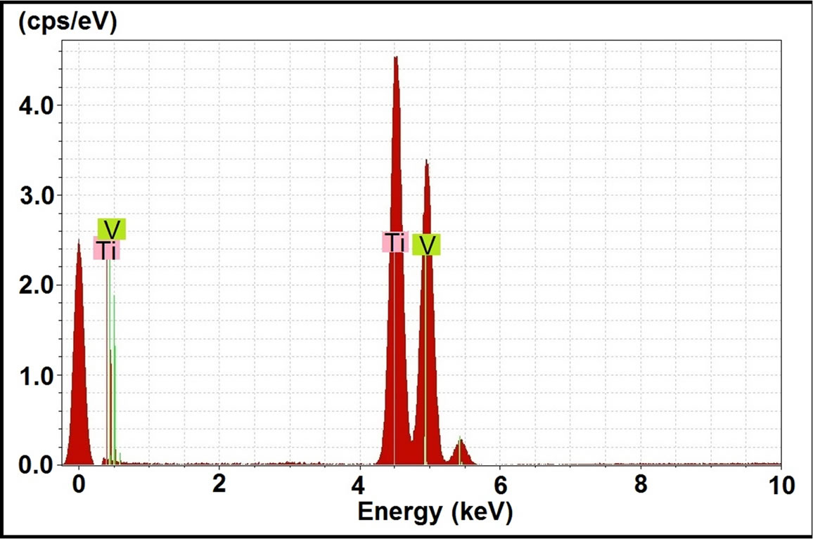
Figure 1. XRF diagram of TiV getter film.
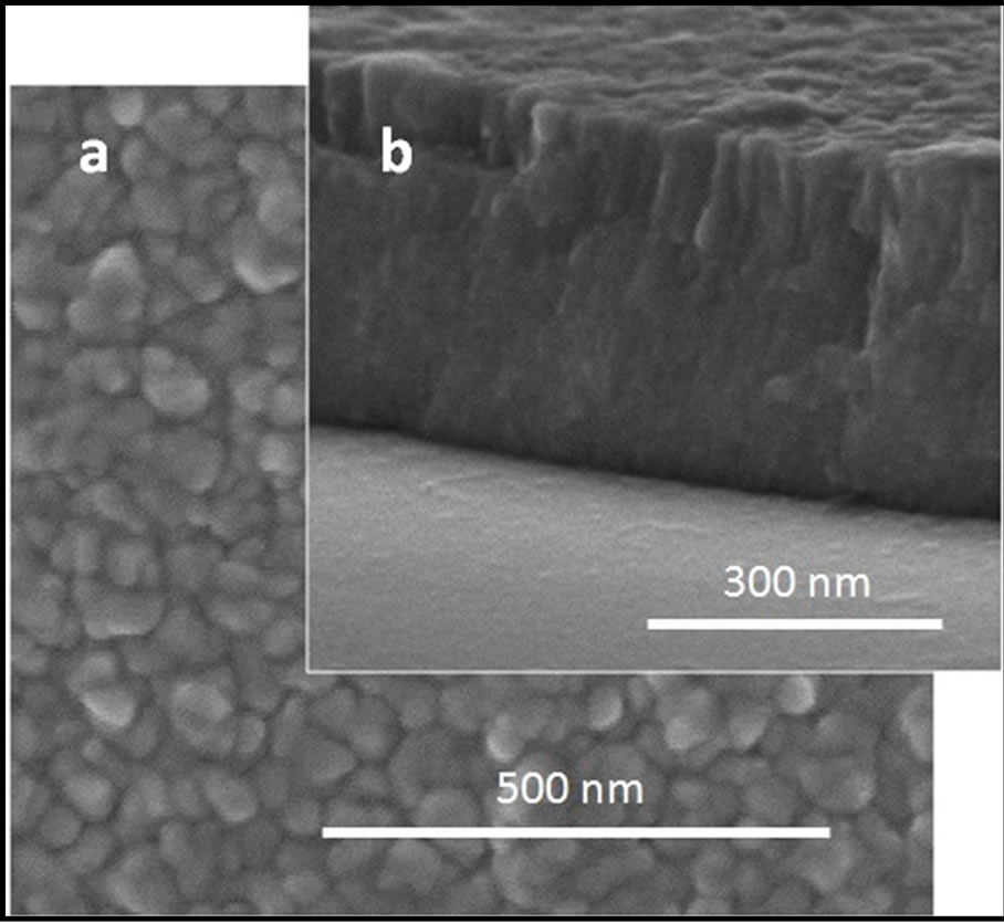
Figure 2. SEM images of the TiV getter film: (a) surface; (b) cross section.
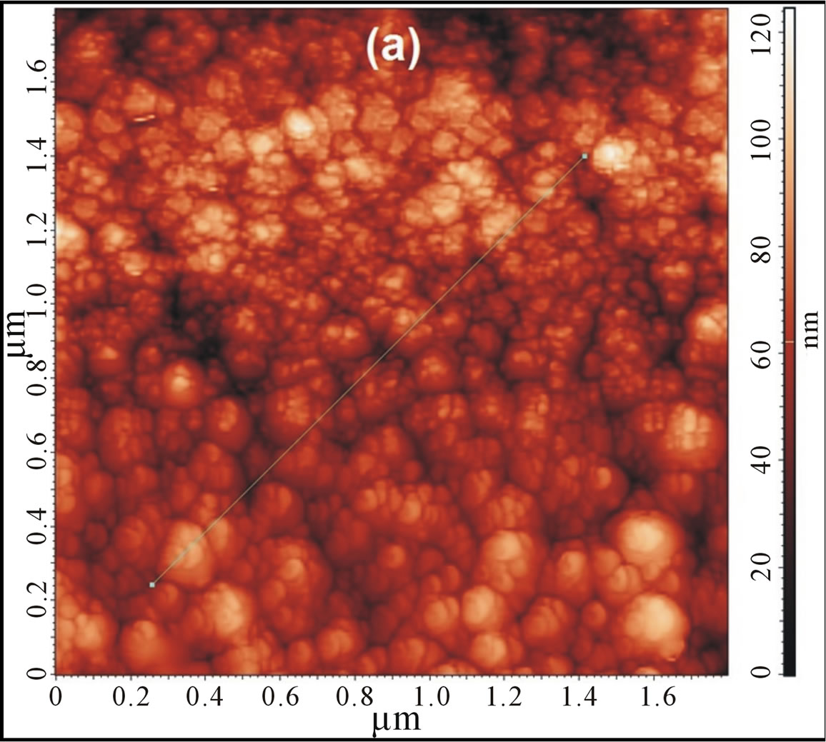
Figure 3. AFM images of the surface (a) and profile AB (b) of getter film produced by magnetron sputtering.
films. The measurement demonstrates the presence of open porosity as well as closed one.
The fractal dimension, allows to characterize the texture quantitatively, was calculated using “perimeter-square” method proposed by Mandelbrot [14]. The structure showed in Figure 2 is characterized by fractal dimension of 2.745 that proves an advanced surface of the sputtered film.
The fractal geometry approaches have been also used for estimation of the grain boundary surface or real surface, which has a large value in the gettering process. The real surface Sreal was calculated according to [15]:
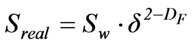 where Sg—geometric surface area; d = 1/256 (256—image resolution); DF—fractal dimension. The computation exhibits real surface area of 155 m2/cm3.
In addition the films have been characterized by sorption capacity measurement using vacuum thermogravimetric method [12]. The samples were activated by heating up to 400˚C at a rate 10˚C /min. After cooling to room temperature the chamber was filled by hydrogen, the pressure of which at 5 × 10⁻³ Pa was sustained. The time dependence graph of relative getter mass when exposed under hydrogen atmosphere is shown in Figure 4. As seen from the graph, the curve of hydrogen absorption is of complex pulsating type that could be interpreted according to [12] as a process of hydride formation in the near-surface region of the getter.
4.2. Composite Structures
The porosity and specific surface of the electrochemically deposited structures have been used by BET method. Adsorption isotherm of N2 at 77 K is shown in Figure 5, where р0—saturation pressure of nitrogen at 77 K.
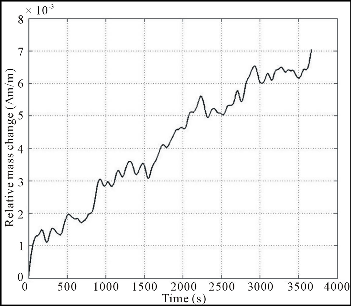
Figure 4. The getter mass alternation during isothermal hydrogen sorption (Т = 20˚C).
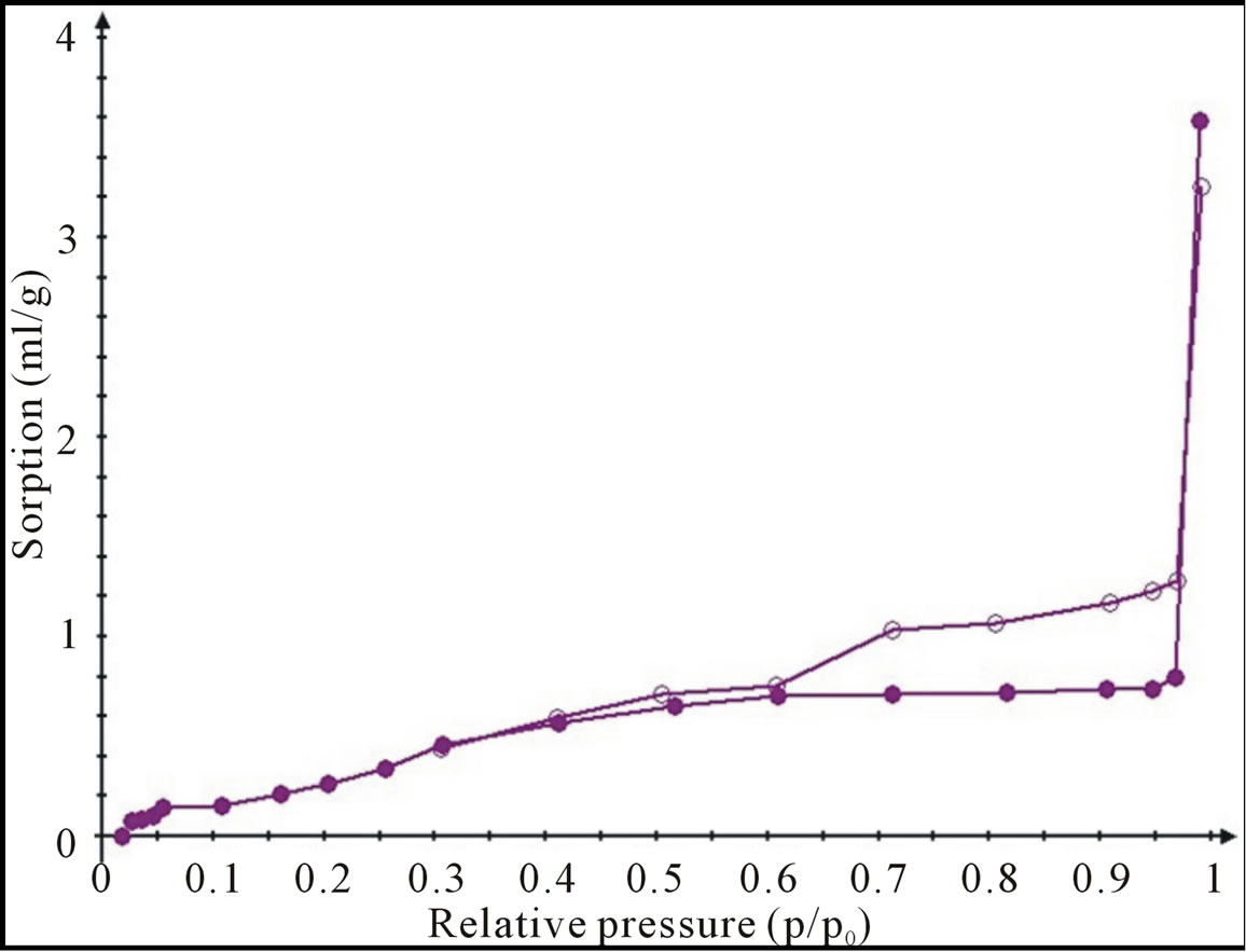
Figure 5. Adsorption isotherm of N2 at 77 K.
The analysis of the adsorption isotherm of shows the importance of the specific surface of the porous layer 0.32 m2/cm2, i.e. actual surface area of the film of 20 µm thick more than 3.000 times greater than the geometrical one, on conversion to a bulk value the specific surface area of the porous layer is about 167 m2/cm3. Examination of the adsorption isotherm gives the film porosity of 60% and average pore diameter of 66.8 nm.
The morphology properties of original structure and generated composite were examined by scanning electron and atomic-force microscopy on different levels of structural hierarchy (Figures 6 and 7). Quasi-periodical metal-silicon structure in Figure 7(a) is in line with the structure of original porous matrix (Figures 6(a) and (b)). Figure 7(b) demonstrates marked self-similar texture of “coral” type, i.e. there are pronounced fractal properties
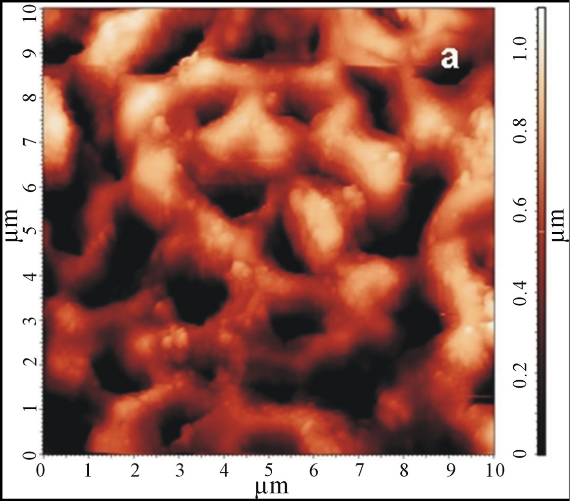
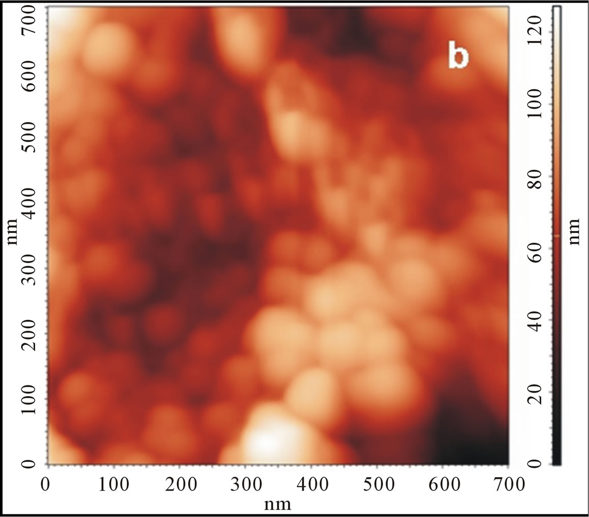
Figure 6. AFM images of the experimental structure of original porous matrix in different scales.
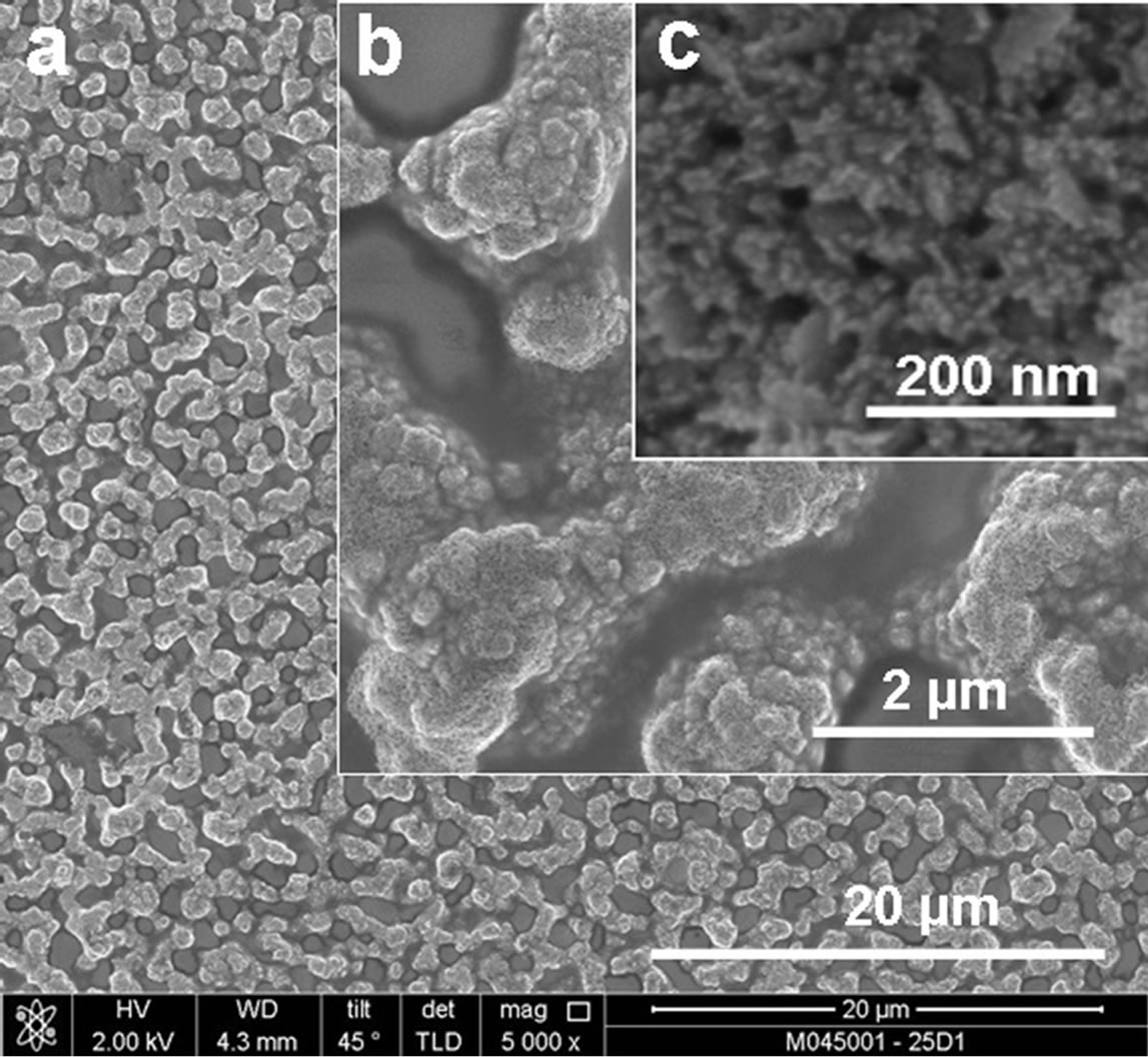
Figure 7. SEM image of the experimental composite structure.
of the deposited layer. As shown by higher resolution, “coral” aggregates consist, in turn, of low-dimensional clusters characterized by grain size of a few nanometers (Figure 7(c)), such a nature of nanoclusters rather defined by the electrodeposition conditions than by the texture of original silicon matrix.
Quantitative estimation of morphological features was made by SEM images processing with the use of fractal analysis tools. The following fractal dimension values of the structures in Figure 7 were calculated: (a) 2.621; (b) 2.624; (c) 2.753. That demonstrates increasing in fractal dimension when images scale decreases, while the high value of the fractal dimension for all the scales remains.
With the use of fractal analysis the real surface area of the composite structure has been calculated and compared with those obtained by BET method. Processing of SEM images in Figure 7 gave the real surface area of 160 m2/cm3, which is in good agreement with the result of BET analysis is of 167 m2/cm3.
The results obtained enable to describe the creation of the composite structure as interaction of the two structure-forming effects. The first is defined by the features of the original porous matrix and how the deposited metal replicates texture of the porous silicon. The second exhibits itself during electrode position; the degree of non-equilibrium of the process determines the probability of growth of dense or granular film. These effects are in a complicated interaction to each other and may be as codirectional and multidirectional depending on the stage of the deposition, metal deposition rate, substrate temperature, the pore size in the porous matrix etc. It can be assumed that probability of dense layer growth increases when deposition rate decreases. At initial growth stages, when deposited layer is enough thin, the texture of the metal film will duplicate the porous silicon one, i.e. so-called isomorphic deposition takes place [9]. In this case the actual surface area of the metal layer approximately corresponds to the surface area of original silicon matrix. Further deposition will plug the small pores and reduce the specific surface given by the porous silicon. In the limit case all the pores are filled by a metal phase and contribution of the silicon structure to open porosity is minimized. On the other hand, an effective surface of the deposited metal film may be more advanced than the surface of the silicon matrix; at a rising of substrate temperature and deposition rate the probability of the growth of granular layer with developed surface is increased.
5. Summary
The study shows that technology of using of porous silicon for structuring of metal layers allows creating composite silicon-metal structures characterized by advanced surface similar to that of layers made by sputtering. The achieved results of specific surface are not ultimate. An improvement of observed technology may give in the issue that the composite structures, which are of effective surface area up to 1000 m2/cm3. This allows us to consider the proposed solutions as a basis for creating getters of a new type as well as other materials demand advanced specific surface.
6. Acknowledgements
The study was supported by the Ministry of science and education of Russian Federation, project No. 14.B37.21.1619.
We thank Anna Bessonova (National Research University of Electronic Technology, Moscow) for the exploration of texture characteristics by BET method.
REFERENCES
- R. Ramesham and R. C. Kullberg, “Review of Vacuum Packaging and Maintenance of MEMS and the Use of Getters Therein,” Journal of Micro/Nanolithography, Vol. 8, No. 3, 2009, Article ID: 031307. doi:10.1117/1.3158064
- A. Corazza and R. C. Kullberg, “Vacuum Maintenance in Hermetically Sealed MEMS Packages,” Proceedings of SPIE 3514, Micromachined Devices and Components IV, Santa Clara, 20 September 1998, pp. 82-90. doi:10.1117/12.323921
- D. Sparks, S. Massoud-Ansari and N. Najafi, “Reliable Vacuum Packaging Using NanoGetters and Glass Frit Bonding,” Proceedings of SPIE 5343, Reliability, Testing, and Characterization of MEMS/MOEMS III, Santa Clara, 24 January 2004. doi:10.1117/12.530414
- R. L. Holtz, V. Provenzano and M. A. Imam, “Overview of Nanophase Metals and Alloys for Gas Sensors, Getters, and Hydrogen Storage,” Nanostructured Materials, Vol. 7, No. 1-2, 1996, pp. 259-264. doi:10.1016/0965-9773(95)00311-8
- A. Prodromides “Non-Evaporable Getter Thin Film Coatings for Vacuum Applications,” EPFL Thesis, Lausanne, 2002, 168 p. doi:10.5075/epfl-thesis-2652
- E. Enqvist, “Synthesis and Characterisation of Non-Evaporable Getter Films Based on Ti, Zr and V,” MS Thesis, Linköpings Universitet, Linköping, 2012.
- C. Benvenuti, P. Chiggiato, P. Costa Pinto, A. Prodromides and V. Ruzinov, “Influence of the Substrate Coating Temperature on the Vacuum Properties of Ti-Zr-V Non-Evaporable Getter Films,” Vacuum, Vol. 71, No. 1-2, 2003, pp. 307-315. doi:10.1016/S0042-207X(02)00755-8
- C. Benvenuti, P. Chiggiato, P. Costa Pinto, A. Escudeiro Santana, T. Hedley, A. Mongelluzzo, V. Ruzinov and I. Wevers, “Vacuum Properties of TiZrV Non-Evaporable Getter Films,” Vacuum, Vol. 60, No. 1-2, 2001, pp. 57-65. doi:10.1016/S0042-207X(00)00246-3
- P. Granitzer and K. Rumpf, “Porous Silicon: A Versatile Host Material,” Materials, Vol. 3, No. 2, 2010, pp. 943- 998. doi:10.3390/ma3020943
- D. Ding, Z. Liu, L. Liu and Z. Li, “A Surface Micromachining Process for Suspended RF-MEMS Applications Using Porous Silicon,” Microsystem Technologies, Vol. 9, No. 6-7, 2003, pp. 470-473. doi:10.1007/s00542-002-0266-7
- W. Mohammad, Ch. Wilson and V. Kaajakari, “Introducing Porous Silicon as a Getter using the Self Aligned Maskless Process to Enhance the Quality Factor of Packaged MEMS Resonators,” 2011 Joint Conference of the IEEE International, San Francisco, 2-5 May 2011, pp. 1- 4. doi:10.1109/FCS.2011.5977875
- A. A. Polunina, “Experimental Determination of the Fine Mechanisms of Absorption of Hydrogen with Titanium to Expand the Range of Performance of Porous Getters,” PhD Thesis, MSIEM, Moscow, 2008.
- S. Brunauer, “The Adsorption of Gases and Vapors,” Vol. 1, Princeton University press, Princeton, 1945.
- B. B. Mandelbrot, “The Fractal Geometry of Nature,” W. H. Freeman and Company, New York, 1982, p. 468.
- N. A. Torkhov, V. G. Bozhkova, I. V. Ivonin and V. A. Novikov, “Determination of the Fractal Dimension for the Epitaxial n-GaAs Surface in the Local Limit,” Semiconductors, Vol. 43, No. 1, 2009, pp. 33-41. doi:10.1134/S1063782609010084
NOTES
*Corresponding author.