Applied Mathematics
Vol.4 No.7(2013), Article ID:34299,5 pages DOI:10.4236/am.2013.47139
Total Harmonic Distortion Minimization of Multilevel Converters Using Genetic Algorithms
Department of Electrical Engineering, Arak University of Technology, Arak, Iran
Email: a_salami@iust.ac.ir, behnam_b60@yahoo.com
Copyright © 2013 A. Salami, B. Bayat. This is an open access article distributed under the Creative Commons Attribution License, which permits unrestricted use, distribution, and reproduction in any medium, provided the original work is properly cited.
Received July 10, 2012; revised January 5, 2013; accepted January 18, 2013
Keywords: Genetic Algorithm; Multilevel Converter Topologies; Multilevel Inverter
ABSTRACT
This paper presents a genetic algorithm (GA) optimization technique to find the optimum switching angles of 11-level inverter with minimum number of dc sources and switches in comparison with the cascade multilevel inverter in order to minimize the total harmonic distortion (THD) of their output voltage waveform. Theoretical and simulation results for an 11-level converter show the efficiency of the proposed algorithm to determine the optimum angles in order to decrease the undesired harmonics and produce very high quality output voltage waveform.
1. Introduction
Multilevel inverters have become an effective and practical solution for increasing the power and reducing the harmonics of AC waveforms. Compared to the traditional two-level voltage source inverters, the stepwise output voltage is the major advantage of multilevel inverters. This advantage results in higher power quality, better electromagnetic compatibility, lower switching losses, higher voltage capability, and needlessness of a transformer at distribution voltage level, thereby reducing the costs [1].
Among The topologies for high power multilevel inverters, the cascaded inverter has the advantages that the DC-link voltage is balanced, the modularized circuit layout is possible, and it has the least components per phase. As the number of levels increases, multilevel inverters have low harmonic components and a low switching frequency, leading to the advent of step-pulse waves that switch once per fundamental cycle. Individual devices operate at high efficiencies because they can switch at a much lower frequency than PWM-controlled inverters [2]. For output step-pulse waveforms, it is necessary to obtain the conducting angles of switching devices. The predominant low-order harmonics can be eliminated. However, it has to solve conventional method has the merit that the simultaneous equations, which are the set of nonlinear transcendental equations for the fundamental component and the harmonic ones. It is difficult to obtain the conducting angles because the conventional method needs an iterative method such as the NewtonRaphson one. Additionally, the switching angles are obtained by means of an off-line calculation to minimize the harmonics for each modulation index, which leads to increased use of look-up tables.
The THD of the output voltage of the inverter is a measurement of the harmonic distortion, which is expected to be as small as possible in many applications of multilevel inverters. One popular example is the singlephase multilevel inverter for the photovoltaic power supply system, in which the THD of the output voltage of the inverter is regarded as a very important measurement of voltage quality [3].
This paper proposes a general genetic algorithm (GA) approach by which the switching angles can be calculated in the context of step modulation for multilevel inverters. This solves the same problem with a simpler formulation and with any number of levels without extensive derivation of analytical expressions. In this paper, the optimization aim of the proposed algorithm is the minimization of the voltage THD. Comparison with other methods also shows that the THD gained by the proposed method is the smallest. Simulation results are given to verify the performance of the proposed method.
2. The Circuit Topology
Figure 1 shows the circuit topology of the 11-level inverter. dc voltage sources are independent each other. Switches Ta, Tb and diode Da are the switches and the

Figure 1. 11 Level inverter.
diode which switch the dc voltage sources in series and in parallel. When the switch Ta becomes off and the switch Tb becomes on, the current flows in the switch Tb and the diode Da, which connect the E voltage sources in parallel. Then, when the switch Ta becomes on and the switches Tb becomes off, the current flows in the switch Ta, which connect the E voltage sources in series via the switch Ta. Using this conversion of dc voltages, outputs 11 levels by v1 + v2 or v1 − v2 [4].
3. Multilevel Inverter with Step Modulation
Various topologies, such as diode clamped multilevel inverters and cascade multilevel inverters, have been applied in industries. An important family of modulation methods for multilevel inverters is the optimal PWM. A representative of this family is step modulation.
Take the example of the 11-level inverter shown in Figure 1, where the basic operation principle of the multilevel inverter and the step modulation strategy is explained. Figure 2 shows the output voltage waveforms of an 11-level inverter under step modulation.  are switching angles that indicate the on or off instant of switches in Figure 1 structure.
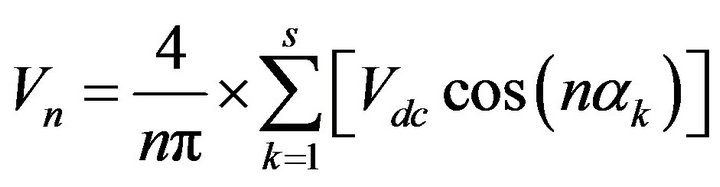
By applying Fourier series analysis for a cascade multilevel inverter with s switching angles, the amplitude of any odd nth harmonic of output voltage can be expressed as:
 (1)
(1)
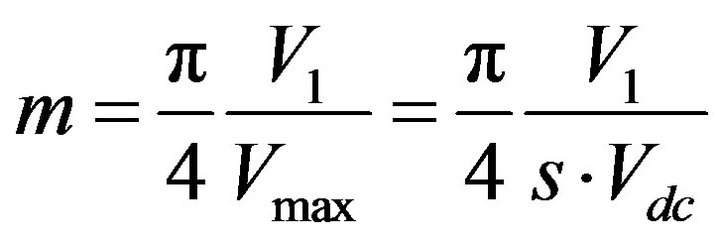
where n is an odd harmonic order and  is the kth switching angle. The amplitudes of all even harmonics are zero. The modulation index m is defined as:
 (2)
(2)
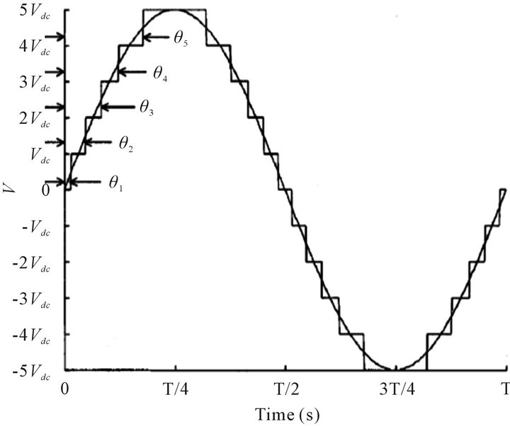
Figure 2. Output voltage of the multilevel inverter and its switching angles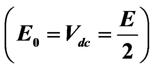 .
.
Vmax is the maximum attainable output voltage of the inverter. In the case of the 11-level inverter, s is five and Vmax is 5 Vdc.
4. Optimization Aim
There are different optimization aims for different applications: 1) minimization of the THD of the output voltage of the inverter, for many applications such as photovoltaic systems [3]; 2) elimination of lower order odd harmonics of the load voltage, such as the third, fifth, and seventh..., for applications equipped with appropriate filters; 3) minimization of the THD but ignoring triple order harmonics that can be cancelled in specific threephase systems [5]; and 4) elimination of lower order odd harmonics but ignoring the triple order harmonics. This paper focuses on the first aim: minimization of the voltage THD. The amplitude of any odd nth harmonic of the output voltage is shown in (3). Thus, the voltage THD is expressed as:
 (3)
(3)
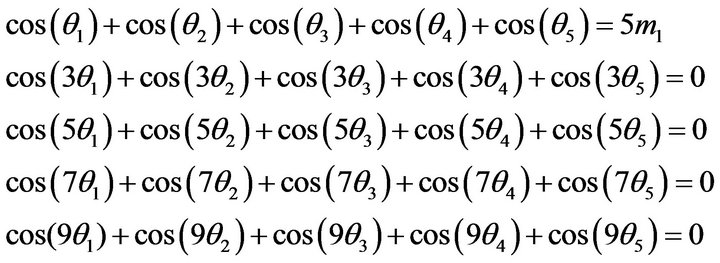
It seems difficult to achieve the minimization of THD directly because the numerator of (3) has infinitely many terms. One solution may be to eliminate only a finite number of harmonics. Generally, one eliminates a few lower order harmonics because they seem to contribute more to THD. In a cascade multilevel inverter with s HBs, only  lower order harmonics could be eliminated. Take the example of an 11-level inverter, the third; fifth, seventh and ninth harmonics can be eliminated as shown in:
 (4)
(4)
several methods, such as Newton-Raphson iteration method [3], methods based on symmetric polynomials and resultants [3], and methods based genetic algorithms [6], have been proposed to solve the nonlinear transcendental equation set as show in (4). In a cascade multilevel inverter with s HBs in the context of step modulation, if more than 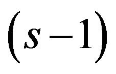 harmonics are considered to minimize THD, these harmonics cannot be eliminated completely since the number of variables is more than the number of equations in the equation set. Minimization of THD in this context has not been investigated until now.
5. Genetic Algorithm (GA)
The aim is to determine the optimum switching angles that generate an output voltage with the required fundamental component and the possible minimum THD. This is a problem to be solved by an optimization algorithm. In this paper, GA is used which is a simple, powerful, and evolutionary technique, inspired from the laws of natural selection and genetics. It is a general-purpose stochastic global search algorithm, with no need of functional derivative information to search for the solutions that minimize (or maximize) a given objective function. GA reduces the computational burden and search time, while solving complex objective functions [5]. To minimizes a function 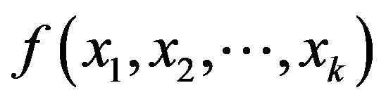 using GA, first, each xi is coded as a binary or floating-point string of length. In this letter, a binary string is preferred, e.g.
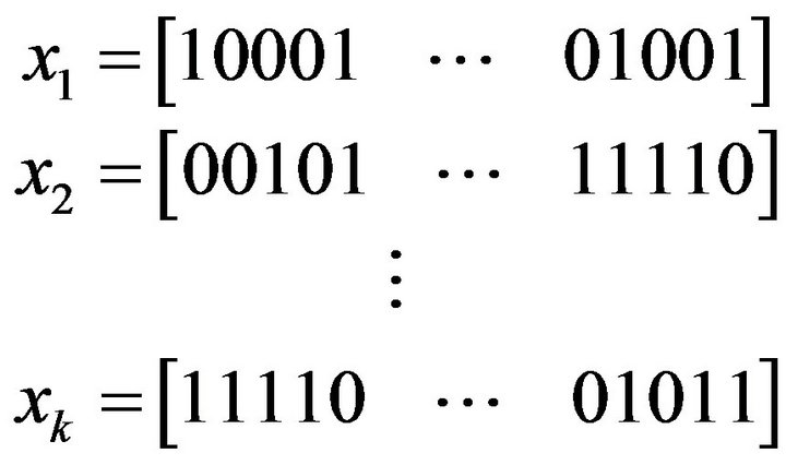
The set 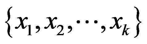 is called a chromosome and xi are genes.
6. Formulation of Problem
The GA methodology is the same for any application. There are only a few parameters to be set for a GA to work. The steps for formulating a problem and applying a GA are as follows:
1) Select binary or floating point strings;
2) Find of the variables specific to the problem; this number will be the number of genes in a chromosome. In this application, the number of variables is the number of controllable switching angles. Each chromosome for eleven-level inverter will have five switching angles, i.e.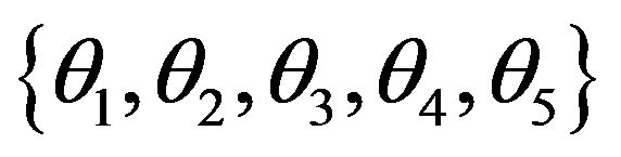 ;
;
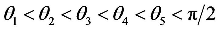
3) Set a population size and initialize the population. Higher population might increase the rate of convergence, but it also increases the execution time. The selection of an optimum-sized population requires some experience in GA. The population in this paper has 20 chromosomes, each containing five switching angles. The population is initialized with random angles between 0 and 90 taking into consideration the quarter-wave symmetry of the output voltage waveform;
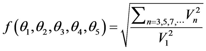
4) The most important item for the GA to evaluate the fitness of each chromosome is the cost function. The objective of this study is to minimize total harmonic distortion of output voltage. Therefore, the cost function f is expressed as:
 (5)
(5)
where  are the switching angles and
  are the n-th order voltage harmonics. For each chromosome, a multilevel output voltage waveform is created using the switching angles in the chromosome. Typically, the GA algorithm is formulated as a maximization problem rather than a minimization problem. In cases where minimization is required, the negative or the reciprocal of the function to be optimized is used. Using this formulation, the fitness value FV is calculated for each chromosome using
 (6)
(6)
The switching angle set producing the maximum FV is the best solution of the first iteration;
5) The GA is usually set to run for a certain number of iterations (100 in this case) to find an answer. After the first iteration, FV’s are used to determine new offspring. These go through crossover and mutation operations and a new population is created which goes through the same cycle starting from FV evaluation. Sometimes, the GA can converge to a solution well before 100 iterations are completed. The solution must also satisfy the following basic constraint:
7. Optimization Aim
To demonstrate the validity of the proposed method, a simulation study was carried out using MATLAB/ SIMULINK. GA is employed to minimize the objective function for the whole range of modulation index. The obtained solutions for optimum switching angles ,
,  are plotted in Figures 3-6 that shows the optimum switching angles when this technique is applied to an 11-level inverter to minimize the THD. For a three-phase load, the line-to-line voltage THD is important, since the triplen harmonics, present in the phase voltage, are eliminated from the line voltage. For the switching angles obtained by Newton-Raphson approach the phase-voltage and line-voltage THD is computed and plotted in Figures 3 and 4 respectively.
With genetic algorithm approach the line-voltage THD and switching angles is computed and plotted versus modulation index in Figures 5 and 6 respectively.

Figure 3. THD versus modulation index of for 11-level 1 phase inverter with Newton-Raphson.

Figure 4. THD versus modulation index of for 11-level 3 phase inverter with Newton-Raphson.
This results show that genetic algorithm is optimized the THD in comparison with Newton-Raphson. The results of two approaches are shown in Table 1" target="_self"> Table 1.
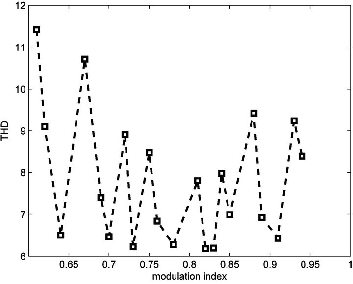
Figure 5. THD versus modulation index of for 11-level inverter with genetic algorithm.
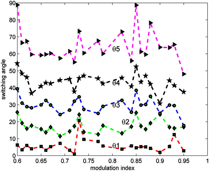
Figure 6. Optimum switching angles versus modulation index of for 11-level inverter.
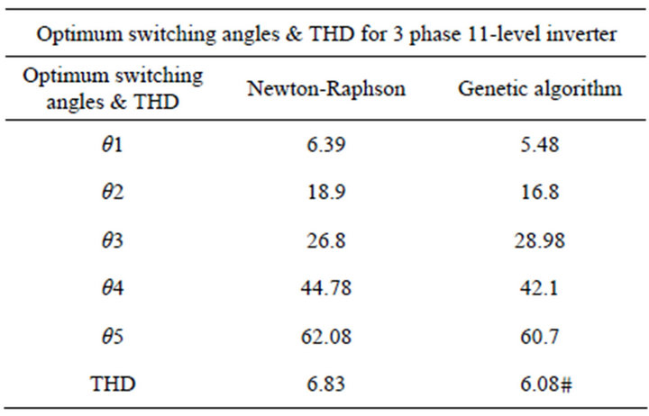
Table 1. Comparison of 2 approaches.
8. Conclusion
This paper has proposed a novel algorithm by which switching angles can be obtained in the context of step modulation for multilevel inverters. With the algorithm, the voltage THD is minimized, which is verified by the THD comparison. The proposed method is able to find the optimum switching angles in a simple manner. The simulation results are provided for an 11-level inverter to validate the accuracy of the computational results.
REFERENCES
- D. W. Kang, H. C. Kim, T. J. Kim and D. S. Hyun, “A Simple Method for Acquiring the Conducting Angle in a Multilevel Cascaded Inverter Using Step Pulse Waves,” IEE Proceedings of Electric Power Applications, Vol. 152, 2005, pp. 103-111.
- H. Taghizadeh and M. Tarafdar Hagh, “Harmonic Elimination of Cascade Multilevel Inverters with Nonequal DC Sources Using Particle Swarm Optimization,” IEEE Transactions on Industrial Electronics, Vol. 57, No. 11, 2010, pp. 3678-3684.
- Y. L. Hoon Hong and A. Q. Huang, “Real-Time Calculation of Switching Angles Minimizing THD for Multilevel Inverters with Step Modulation,” IEEE Transactions on Industrial Electronics, Vol. 56, No. 2, 2009, pp. 285-293. doi:10.1109/TIE.2008.918461
- Y. Hinago and H. Koizumi, “A Single Phase Multilevel Inverter Using Switched Series/Parallel DC Voltage Sources,” 2009 IEEE Energy Conversion Congress and Exposition (ECCE 2009), San Jose, 20-24 September 2009.
- B. Ozpineci, L. M. Tolbert and J. N. Chiasson, “Harmonic Optimization of Multilevel Converters Using Genetic Algorithms,” IEEE Power Electronics Letters, Vol. 3, No. 3, 2005, pp. 92-95. doi:10.1109/LPEL.2005.856713
- N. Yousefpoor, S. H. Fathi, N. Farokhnia and H. Askarian Abyaneh, “THD Minimization Applied Directly on the Line-to-Line Voltage of Multilevel Inverters,” IEEE Transactions on Industrial Electronics, Vol. 59, No. 1, 2012, pp. 373-380.