Journal of Signal and Information Processing
Vol.4 No.2(2013), Article ID:30994,5 pages DOI:10.4236/jsip.2013.42018
Design of a Novel Front-End Readout ASIC for PET Imaging System*
![]()
School of Computer Science and Technology, Northwestern Polytechnical University, Xi’an, China.
Email: shykongxin@163.com
Copyright © 2013 Huiming Zeng et al. This is an open access article distributed under the Creative Commons Attribution License, which permits unrestricted use, distribution, and reproduction in any medium, provided the original work is properly cited.
Received March 18th, 2013; revised April 20th, 2013; accepted April 29th, 2013
Keywords: PET; Front-End Readout Electronics; TDC; Positron Emission Tomography Imaging
ABSTRACT
The architecture of a multi-channel front-end system is important for realizing a high-resolution PET system. We propose a novel front-end readout electronic system with TDC to deal with time information for PET system which can easily design the timing control. Each channel consists of a charge preamplifier, slow/fast shaper, discriminator and a analog memory. There are a ADC and a TDC to process the energy information and time information for each channel at the same time. In this paper, the whole system signals flow is all simulated by MATLAB. The simulation results show that the proposed system can process slender current from the detector and achieve the energy and time information. The proposed architecture can be applied to high-resolution PET imaging systems with multi-channel ASICs.
1. Introduction
Positron emission tomography imaging technic is one of the tiptop imaging technique in biomedical imaging. PET imaging facilities came through much momentous change in the past thirty years. At present, three dimension PET imaging and TOF (time of flight) PET imaging facilities have been used in clinical experiments [1,2]. But as the fast development of PET imaging, PET/CT and magnetic resonance imaging (MRI) and 4-D PET imaging research still have been undertaken.
The research of PET begins at 1980s, but with the revolutionary change of the technology and methods, the front-end circuit developed with the development of the detector of PET system [3,4]. Furthermore, the developing way of PET system is the improvement of the spatial resolution, sensitive and the detection efficiency. The improvements of computing, especially the improvement of the ADC, accelerate the development of PET system and lead to the optimization and revolution of the frontend circuit. With the development of CMOS technology, such as decrease of the minimum line width and threedimensional integrated technology, the performance, design method and cost of the front-end specific chip are advanced constantly [5,6].
This paper discussed a novel front-end readout circuit architecture and design challenges for PET imaging systems, and gave the simulation results for signals flow. The proposed architecture can be applied to high-resolution PET imaging systems with multi-channel ASICs.
2. PET Imaging System
Front-end microelectronics for PET imaging is a complex system which deals with analog/composite signal, this circuit including charge-sensitive amplifier, shaper circuit, time-stamp circuit, peak detector, data convert circuit and so on. The signal detected by the detector is very weak, so pulse height analysis is needed. The weak signal must be amplified, shaped and then detected peak. Meanwhile, we must stamp the time when the photon arrived the detector. The discriminator is used to sample and distinguish the time signal on the sequence. Moreover, for digital processing, the power signal and time signal need to be converted by specific digital circuit. The digital circuit includes ADC and TDC which is multi-channel, low power consumption. The digitized signal is stored, pre-process and transferred by the followed circuit. The data of multiple channels need to sync by protocols such as TCP/IP, transfer by optical fiber and deal by computer.
In this proposed system, the detector module consists of LYSO crystals coupled with silicon photomultiplier. We do not need a low noise front-end readout circuits to deal with this pulse. In our solution, a charge preamplifier is proposed to collect the current signals in all channels due to its high sensitivity. Thus the crosstalk between channels can be decreased. The peak values of the shaped pulses are digitized by a pipeline ADC in serial. The triggers are sent to a high-precision TDC. The prospective energy resolution is 96 fC, time resolution is 20 ps, and SNR > 20 dB.
3. Proposed Front-End ASIC Architecture
The proposed architecture of the front-end readout ASIC is shown in Figure 1. JTAG is a test module to validate the performance and the correctness of the circuits. The BIAS module is to offer bias for whole system. The ADC and TDC are to deal with the energy information and time information from the multi-channel.
The architecture of each channel is shown in Figure 2. The principle of each channel is described as followings. Each detector connects to an 8-bit DAC to steady the voltage of the silicon photomultiplier which can make the detector work in a stabilestate. The valid signal of the silicon photo multiplierthen is sent to a low gain charge preamplifier to collect and amplify the signal from the detector. The photon electron dynamic range offered by preamplifier is from 1to 2000, and the noise level is 1/10 photon electron. The electric information from the preamplifier is sent separately into two different channels. The one channel is to store the energy information. In the energy measure channel, the input signal is to a shaper which the shaping time range is from 50 ns to 100 ns. The signal wave after shaping is delivered to the analog memory, and through the sample and hold operation in the analog memory the peak value is detected, in other words, the peak value is the energy information. Afterward the energy information is proceeded by the ADC. The other channel is to store the time information. In the time measure channel, the input signal is to a shaper which the shaping time range is 15 ns. The signal wave after shaping is delivered to the discriminator to be compared to the referenced current. In the sequel, the time information is proceeded by TDC. In the system, we introduce a 10-bit pipeline ADC and 20 ps TDC to proceeded the analog signals. The special characteristic of the proposed system is easy to control the working timing compared to the reference [7].
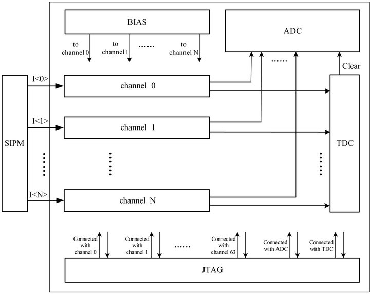
Figure 1. Proposed ASIC system structure.
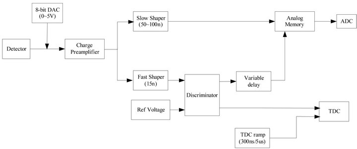
Figure 2. Single-channel scheme.
The main difference to the reference [7] is that the multi-channel system architecture and the method to deal with the time information. In the proposed system, we separately proceed the energy and time information by a ADC and a TDC. In this way, we can proceed the energy and time information at the same time which can predigestthe control timing and speedup the system work. The front-end readout system proposed in the paper has the following characteristics:
The connection way of silicon photomultiplier and front-end readout circuits. The stability processing between the detector and the circuits can make the silicon photomultiplier work in the same work state, which can offer the preamplifier stable signals.
Added fast shaper in the time measure channel. Making use of the past zero character of the fast shaper to avoid the error generated by the Time Walk. This method can reduce the mistake by time trigger.
Added a 10-bit DAC and a 4-bit DAC to obtainprecise base voltage of the discriminator. The 10-bit DAC is used to coarsely adjust the base voltage and the 4-bit DAC is used to finely adjust the base voltage.
Quantized the time information to expediently digital proceeding. Added a TDC ramp to enlarge the time measure range, sequentially enhance the veracity. The height and the scope of the TDC ramp can lead to different results.
Energy and time information are collected respectively by ADC and TDC. This method can easily to design timing control, simplify the circuits, speedup the system work. Moreover, the method can improve the space resolution and the imaging quality.
4. Simulation Results and Discussion
The whole front-end readout system consists of a charge preamplifier, a slow shaper (shaping time 50 ns - 100 ns)a fast shaper (shaping time 15 ns), a 10-bit pipeline ADC, a 20 ps TDC and a high precisiondiscriminator. All of the circuits is simulated by MATLAB. The detector is modeling to the model as Figure 3. As Figure 3 showing, approximately, the detector equals to a current sourceparallel connected to an internal resistance and aparasitical capacitance. The current source signal is adopted Dirac’s delta pulse [1].
The input of charge preamplifier here is from 0.5 uA to 10 uA. The leak current is set to 0.5 uA. Figure 4 shows the simulation result of the charge preamplifier. From the result we can see that charge preamplifier can exactly collect the charge information. Figure 5 presents the step response of shaper. Figure 6 gives the simulation result of sample and hole circuit. The simulation results of discriminator are shown in Figure 7. Figure 8 shows the result of the 10-bit pipeline ADC. Figure 9 is the simulation result of TDC.
The results show that the system can deal with the weak signal from the detector and gain the energy and time information for the imaging. And validate the validity of the front-end readout circuits. Of course, every system has its disadvantage, so does the proposed ASIC structure. The performance of PET imaging systems rests with the capability of front-end readout and signal processing electronic elements. Especially, the front-end signal processing circuit is directly related to the quality of final imaging pictures. The circuits must satisfy the requirement of radiation hardening and must be high speed and low error probability. Besides, to the front-end readout circuit used in nuclear radiation detector, low power dissipation even zero power dissipation will be the necessary conditions. Thus, the boundary of low power dissipation brings considerable challenges to circuit design. Multicenter TDC used in picoseconds level resolution time measure. TDC is one of the most difficult circuits in
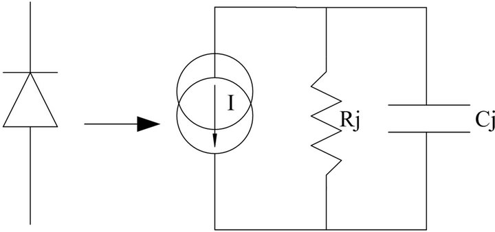
Figure 3. Equal model of the detector.
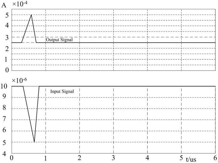
Figure 4. Simulation result of preamplifier.
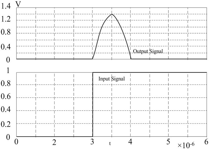
Figure 5. Step response of shaper.
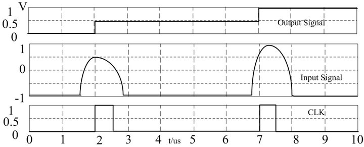
Figure 6. Simulaton result of sample and hold circuit.
data converter, and the resolution measured is confined by circuit structure, noise, temperature and so on. When

Figure 7. Simulaton result of discriminator.
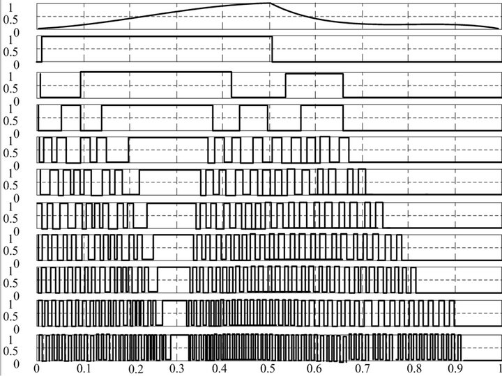
Figure 8. Simulaton result of 10-bit pipeline ADC.
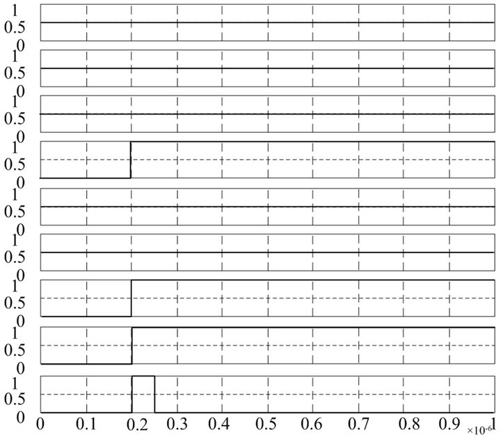
Figure 9. Simulaton result of TDC.
the measured time interval drops to several or several tens picoseconds, circuit design practically needs to use the design method of radio frequency circuit. Highresolution multiple-channel energy peek value detecting and digital-converting circuit. This part circuit refers to signal sample and hold, analog to digital converting, digital signal storage and transfer. ADC generally requires 10 bits above resolution, and the conversion strategy depends on the need of practical data collection.
The main disadvantage of the proposed ASIC scheme is that in this system the bias must be designed in all the module when do simulations, so the next work is to design the bias for all the circuits.
5. Consolation
A novel front-end readout ASIC structure for PET imaging system is proposed in the paper. The photon electrondynamic range offered by preamplifier is from 1 to 2000, and the noise level is 1/10 photon electron. The prospective energy resolution is 96 fC, time resolution is 20 ps, and SNR > 20 dB. From the simulated results, the proposed structure can satisfy the requirements of the PET systems. The proposed architecture can be applied to high-resolution PET imaging systems with multichannel ASICs.
REFERENCES
- M. S. Judenhofer, H. F. Wehrl, D. F. Newport, et al., “Simultaneous PET-MRI: A New Approach for Functional and Morphological Imaging,” Nature Medicine, Vol. 14, 2008, pp. 459-465. doi:10.1038/nm1700
- F. Corsi, M. Foresta, C. Marzocca, et al., “A Self-Triggered CMOS Front-End for Silicon-Multiplier Detectors,” 2009.
- F. Corsi, C. Marzocca, A. Perrotta, et al., “Electrical Characterization of Silicon Photo-Multiplier Detectors for Optimal Front-End Design,” 2006.
- B. F. Aull, A. H. Loomis, D. J. Young, et al., “GeigerMode Avalanche Photodiodes for Three-Dimensional Imaging,” 2002.
- F. Habte and C. S. Levin, “Study of Low Noise MultiChannel Readout Electronics for High Sensitivity PET Systems Based on Avalanche Photodiode Arrays,” IEEE Transactions on Nuclear Science, Vol. 51, No. 3, 2004, pp. 764-769. doi:10.1109/TNS.2004.829599
- J. F. Pratte, G. De Geronimo, S. Junnarkar, et al., “FrontEnd Electronics for the RatCAP Mobile Animal PET Scanner,” IEEE Transactions on Nuclear Science, Vol. 51, No. 4, 2004, pp. 1318-1323. doi:10.1109/TNS.2004.832299
- J. D. Martinez, J. M. Benlloch, J. Cerda, et al., “HighSpeed Data Acquisition and Digital Signal Processing System for PET Imaging Techniques Applied to Mammography,” IEEE Transactions on Nuclear Science, Vol. 51, No. 3, 2004, pp. 407-412. doi:10.1109/TNS.2004.828531
NOTES
*This work is supported by the National Natural Science Foundation of China (No. 60972157) and graduate starting seed fund of Northwestern Poly Technical University (No. Z2011122).