Wireless Engineering and Technology
Vol.4 No.2(2013), Article ID:29806,7 pages DOI:10.4236/wet.2013.42016
Design and Parametric Simulation of a Miniaturized PIFA Antenna for the PCS Band
![]()
1Department of Electrical and Telecommunications Engineering, Royal Air Academy (ERA), Marrakesh, Morocco; 2Department of Physics, Semlalia University of Sciences (FSSM), Marrakesh, Morocco.
Email: elouadih@gmail.com, a_ouladsaid@hotmail.com, hassani@ucam.ac.ma
Copyright © 2013 Abdelhakim Elouadih et al. This is an open access article distributed under the Creative Commons Attribution License, which permits unrestricted use, distribution, and reproduction in any medium, provided the original work is properly cited.
Received February 9th, 2013; revised March 10th, 2013; accepted March 18th, 2013
Keywords: PCS; HFSS; PIFA; Patch Antenna; Parametric; Simulation
ABSTRACT
This paper describes the design and simulation by HFSS simulator of a probe-fed Planar Inverted-F Antenna (PIFA) for the use in PCS band [1850 MHz - 1990 MHz]. A methodology based on parametric simulations (parameters are ground plan dimensions, height of radiating plate, feeding point position, shorting plate dimensions and positioning) was used to design optimized antenna. The simulation allowed the characterization of the designed antenna and the computing of different antenna parameters like S11 parameter, resonant frequency, SWR, bandwidth impedance in feeding point, gain, 2D and 3D diagram pattern, Fields distribution. The simulation results are interesting and respect the mean PCS requirements.
1. Introduction
Wireless communications have progressed very rapidly in recent years, and many mobile units are becoming smaller and smaller. To meet the miniaturization requirement, the antennas employed in mobile terminals must have their dimensions reduced accordingly. Planar antennas, such as microstrip and printed antennas have the attractive features of low profile, small size, and conformability to mounting hosts and are very promising candidates for satisfying this design consideration. Planar antennas are also very attractive for applications in communication devices for wide mobile telecommunications like GSM 1900 called PCS (Personal Communications System), wireless local area network, aeronautics and embedded systems [1].
For optimum system performance, the antennas must have high radiation efficiency, small volume, isotropic radiation characteristics, small backward radiation and SAR, simple and low-loss impedance matching to patches. The major types of configurations of low-profile antennas with enhanced bandwidth performance include planar inverted F Antennas.
The PIFA consists in general of a ground plane, a top plate element, a feed wire attached between the ground plane and the top plate, and a shorting wire or strip that is connected between the ground plane and the top plate.
The antenna is fed at the base of the feed wire at the point where the wire connects to the ground plane. The PIFA is an attractive antenna for wireless systems where the space volume of the antenna is quite limited. It requires simple manufacturing, since the radiator must only be printed. The addition of a shorting strip allows good impedance match to be achieved with a top plate that is typically less than λ/4 long. The resulting PIFA is more compact than a conventional half-wavelength probe-fed patch antenna [2].
The miniaturization can affect radiation characteristics, bandwidth, gain, radiation efficiency and polarization purity. The miniaturization approaches are based on either geometric manipulation (the use of bend forms, meandered lines, PIFA shape, varying distance between feeder and short plate [3]) or material manipulation (loading with a high-dielectric material, lumped elements, conductors, capacitors, short plate [4]) or the environment characteristics (ground plane dimensions, coupling, measurement and fabrication errors [3]). In this case, the designed antenna is shorted to the ground plane by a plate, uses regular shapes and a high dielectric thin substrate under the radiating plate not above the ground plane.
If all precedent works are concentrated on studying the effects of these elements (material, geometry, environment), the choice of a PIFA element is so improvised in the design. In this paper, a methodology based on parametric simulation is used to choose simultaneously or independently different PIFA elements.
In the next section, the author presents the methodology and detailed parametric simulations to optimize the antenna design. After, the dimensions and parameters are then chosen. The author exposes the characteristics of the designed antenna in the third section.
2. Design Methodology
2.1. The Description of the Studied Antenna
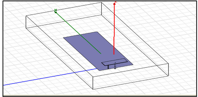
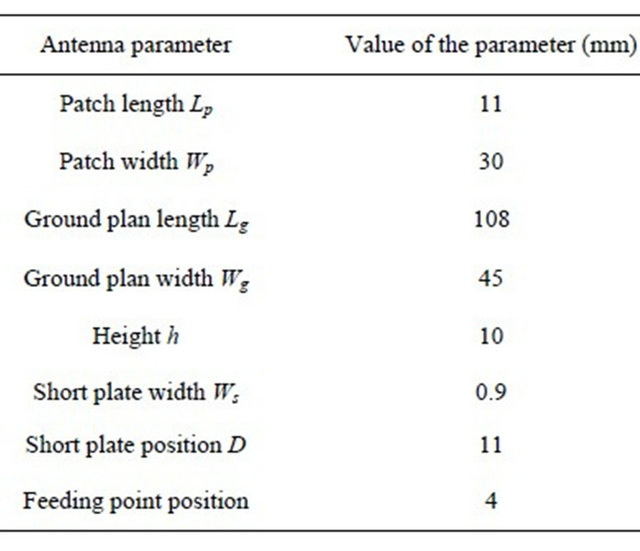
As shown in Figure 1, the designed antenna has a rectangular radiating patch witch length is Lp = 11 mm and width Wp = 30 mm. The patch in placed at a height h from the ground plan. The last has a length Lg and a width Wg. The patch is matched to the ground plan via a rectangular shorting plate. The shorting plate has a width Ws and a length Ls. The shorting post of usual PIFA types is a good method for reducing the antenna size, but results in narrow impedance bandwidth. It is placed in the (yz) plan at a distance D from the edge centre and a distance p from the feeding point. The patch is fed by a 50 Ω wire; a semi-rigid coax with a centre conductor that extends beyond the end of the outer conductor is used to form the PIFA feed wire. The outer conductor of the coax is sol-
 (a)
(a)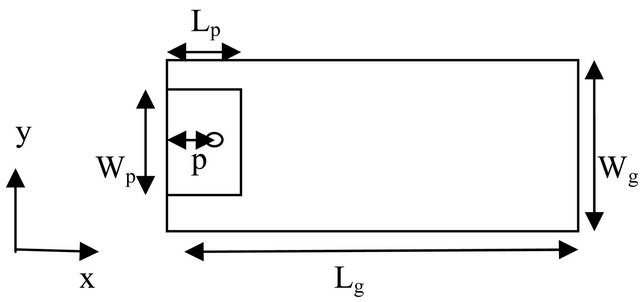 (b)
(b)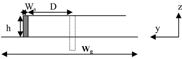 (c)
(c)
Figure 1. The designed antenna by HFSS. (a) Perspective view; (b) Top view; (c) Side view.
dered to the edge of a small hole drilled in the ground plane at the feed point. The volume between the radiating plate and the ground plan is filled by air except a thin region 0.8 mm under the radiating patch who is composed of FR4_epoxy (εr = 4.4).
2.2. The Choice of the Patch Dimensions
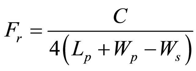
It is very important for simulation by HFSS to estimate the resonant frequency that help the simulator to make a refinement mesh in a band around the resonant frequency and then give more precise values. The resonant frequency of a PIFA is approximated by the Equation (1) where Fr is the resonant frequency, C is the light velocity.
 (1)
(1)
If there is another substrate different from Air, C will be , where
 . For our case, the space between the patch and the ground plan is essentially air minus a 0.8 mm FR4 epoxy layer.
To compute the resonant frequency, we have the following values: Lp = 11 mm, Wp = 30 mm,  = 1 mm. We obtain: Fr = 1875 MHz.
The obtained frequency is then not far from 1920 MHz the central frequency of PCS band. In fact, there is no equation to determine the resonant frequency for a PIFA that contains not only the patch dimensions but also the other parameters that can affect the antenna characteristics. For this, the author will make constant the patch dimensions that are the mean parameters can furnish the resonant frequency and he will vary undependably the other parameters (ground plan dimensions Lg and Wg, height of radiating plate h, feeding point position p, shorting plate width Ws and position D).
2.3. The Choice of the Simulator
HFSS (High Frequency Simulator Structure) is a high performance full wave electromagnetic (EM) field simulator for arbitrary 3D volumetric passive device modeling that takes advantage of the familiar Microsoft Windows graphical user interface. It integrates simulation, visualization, solid modeling, and automation are easy to learn environment where solutions to 3D EM problems are quickly and accurate obtained. Ansoft HFSS employs the Finite Element Method (FEM), adaptive meshing, and brilliant graphics to give unparalleled performance and insight to all of 3D EM problems. Ansoft HFSS can be used to calculate parameters such as S-Parameters, Resonant Frequency and Fields. Typical uses include Package Modeling, PCB Board Modeling, Mobile Communications (Patches, Dipoles, Horns, Conformal Cell Phone Antennas), Specific Absorption Rate (SAR), Infinite Arrays, Radar Section (RCS), Frequency Selective Surface (FSS) and filters such Cavity Filters, Microstrip, Dielectric. HFSS is an interactive simulation system whose basic mesh element is a tetrahedron T. In industry, Ansoft HFSS is the tool of choice for High productivity research, development, and virtual prototyping [5,6]. The HFSS is then used in our simulation; the author proposes after to expose the results of the HFSS simulations.
2.4. The Choice of the Height h
The height h is the distance between the top plate and the ground plane. In order to eliminate the effects of the ground plane effects, we place the patch on the edge of an infinite ground plane at a height varying from 6 mm to 13 mm. From the simulation result shown by Figure 2, the optimal height h is for h = 10 mm because it gives values S11 most important and closer to central frequency.
2.5. The Choice of the Ground Plan Width Wg
For the height equal to 10 mm, we will vary the groundplane width by having a very important length Lg to eliminate its effect. In general, the width Wg is not so far to Wp that is the minimum. For this, Wg will vary from 30 mm to 60 mm. the simulation result is shown by Figure 3. We can consider Wg = 45 mm an optimal width because it presents the minimum S11 for all the band and

Figure 2. Parametric simulation by varying h.
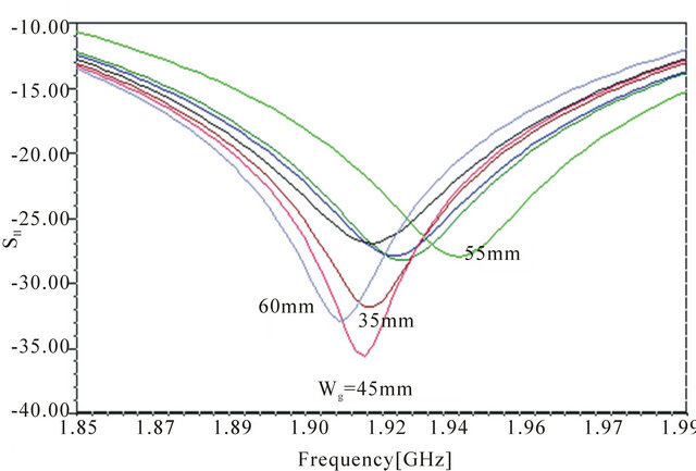
Figure 3. Parametric simulation by varying Wg.
in the same time the minimum is the closest to the central frequency in the PCS band.
2.6. The Choice of the Ground Plan Length Lg
The height h in now 10 mm and the Wg is 45 mm. We will vary the ground plane length Lg from 60 mm to 140 mm. This sweep is taken because the designed antenna will be mounted on a GSM handset. The Figure 4 shows the result of the parametric simulation. We can see from the curve that the length 100 mm is the most adapted. In reality, the simulation shows close results for the lengths 100 mm, 110 mm and 120 mm. A sweep refinement is introduced and the optimum was 108 mm. Also, 120 mm and over can be considered not interesting values for a ground plane in a handset. We have then h = 10 mm, Wg = 45 mm and Lg = 100 mm. We will after simulate the effect of the shorting element width Ws and distance D from the patch edge centre.
2.7. The Choice of the Shorting Plate Position D
We will vary the shorting plate position between all possible values from 0 to 14 mm, we width Ws is in general close to 1 mm. we obtain the result shown by Figure 5. Both of positions 11 and 12 mm gibe good result. We can choose D = 11 mm, it’s closer to the central frequency.
2.8. The Choice of the Shorting Plate Width Ws
We will vary the width Ws from 0.5 to 3 mm with step of 0.5 mm. We will obtain the result shown by Figure 6. We can consider the width Ws = 1 mm the most convenient for the bandwidth and the resonant frequency. From the curve, the width Ws is close to 1 mm. If we make a sweep refinement by choosing 0.1 mm step instead of 0.5 mm in order to hope having a S11 peak near the central frequency if possible. We obtained the result shown by Figure 7. We can remark a net peak for the particular
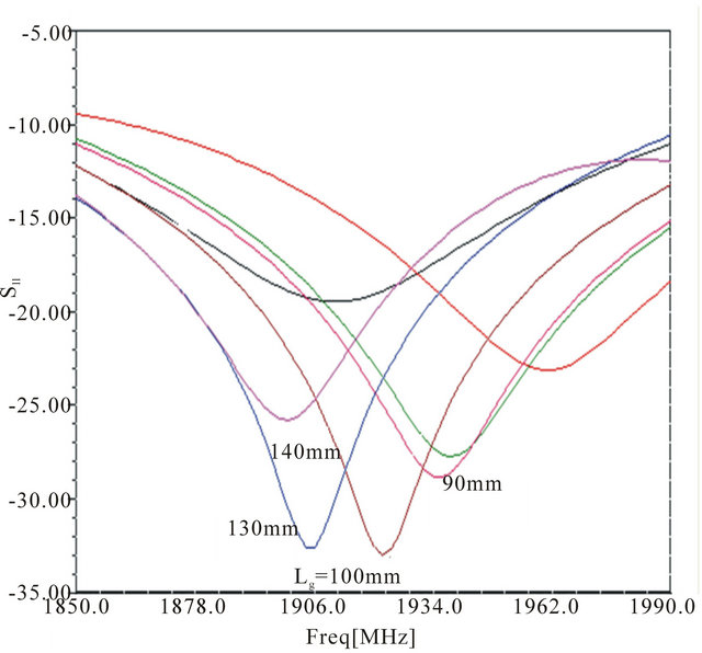
Figure 4. Parametric simulation by varying Lg.
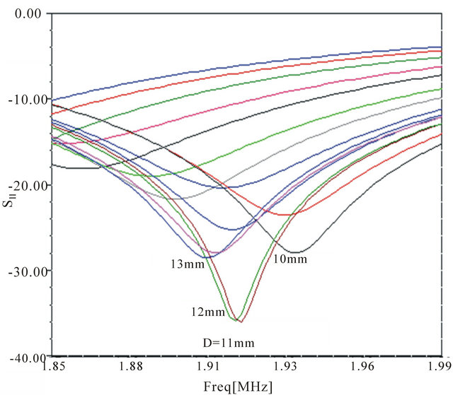
Figure 5. Parametric simulation by varying D.
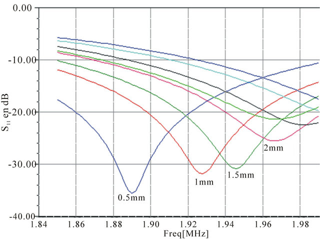
Figure 6. Parametric simulation by varying Ws (step = 0.5 mm).
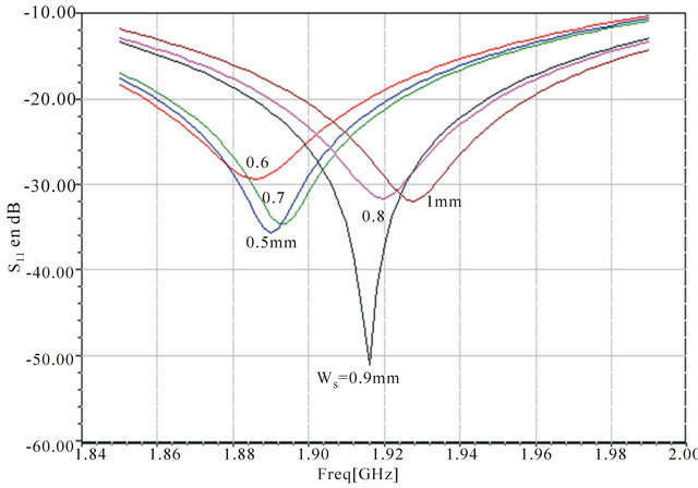
Figure 7. Parametric simulation by varying Ws (step = 0.1 mm).
value of 0.9 mm. For all studied parameters, any linear relation can’t be established between bandwidth enhancement and the parameter variation. We have then chosen the parameters h, Lg, Wg, D and Ws. We can now look for the effect of the feeding point position p to enhance the bandwidth or the input impedance.
2.9. The Choice of the Feeding Point Position p
The feeding point position p is calculated from the rear edge of the patch. We will vary the p parameter from 2 mm to 10 mm we mean all possible cases. The values 1 and 11 mm can’t be taken because the feeding point is theoretically a circle that has a radius. The result is shown on Figure 8. We can consider the peak for p = 4 mm an interesting position for feeding.
3. The Designed Antenna Characterization
The dimensions of the designed antenna for the PCS band are summarized in the Table 1. We will now present the antenna characteristics.
3.1. The Reflection Loss
The Figure 9 shows the S11 parameter function of frequency in [0 - 3 GHz]. We can see a peak of S11 parameter around 1924 MHz very close to the PCS central frequency 1920 MHz. Also, the S11 values out of the PCS band are near 0 that means the designed antenna can’t interfere with other radiations. We can also run the si-
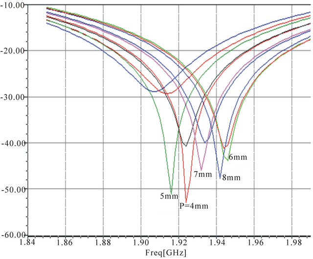
Figure 8. Parametric simulation by varying p.
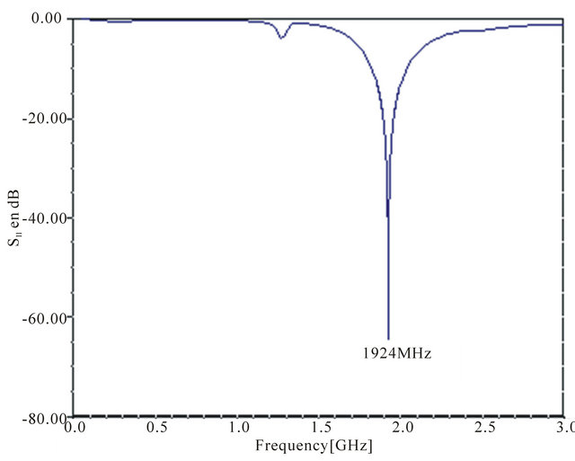
Figure 9. S11 depending on frequency for [0 - 3 GHz].
mulation by refining the sweep interval for more precision and as shown in Figure 10. The Figure 11 furnished by the simulation gives exactly S11 = −12.43 dB for 1850 MHz (the low frequency of the PCS band), S11 = −60 dB for 1925 MHz (the peak frequency), the simulation tables give exactly a peak of −64.46 dB for the frequency 1924.7 MHz and S11 = −12.49 dB for 1990 MHz (the high frequency of the PCS band). For the whole PCS band, the designed antenna has a S11 litter than −12.4 dB. It is very interesting result.
3.2. The VSWR and Bandwidth
We obtain as shown in Figure 12(a) VSWR = 1.62 for 1850 MHz (the lowest frequency of the PCS band), VSWRmin = 1.001 for 1924.7 MHz (the peak frequency), VSWR = 1.49 for 1990 MHz (the highest frequency of the PCS band). The VSWR is at its minimum, it’s a very interesting result. Also, the PCS bandwidth (140 MHz) is for the designed antenna a 1:1.62 VSWR bandwidth. It is considered a very interesting result.
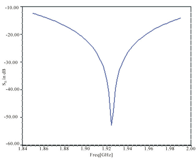
Figure 10. S11 depending on frequency for PCS band.
Table 1. The designed antenna dimensions.
The designed antenna presents a 1:1.5 VSWR bandwidth equal to 130 MHz.
3.3. The Smith Chart
The Figure 13 shows a regular smith chart with interesting parameters of reflection, impedance, VSWR, and Q. The feeding point impedance for extremes and central frequencies are given in Table 2.
3.4. Antenna Parameters
The simulations results shown in Figure 14 give the antenna parameters. The obtained gain G is 1.16 dBi and the radiation efficiency is 1.0085.
3.5. The Diagram Pattern
We can confirm by the Figure 15 that (xz) is the E-plane and its maximum is for (phi = 0 deg et theta = 56 deg). Also, we can verify that via the 3D polar diagram shown in Figure 16.
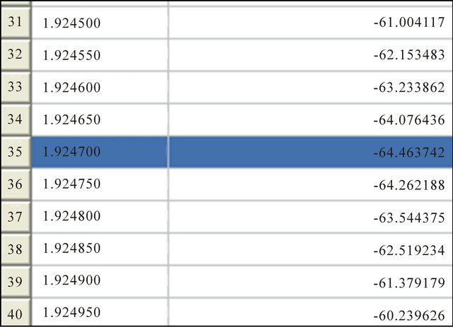
Figure 11. The resonant frequency.
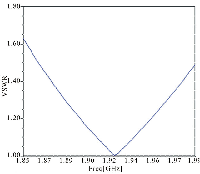
Figure 12. The VSWR depending on the frequency for the PCS band.
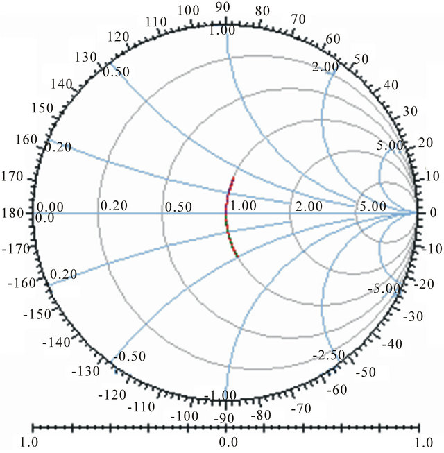
Figure 13. The smith chart for PCS band.
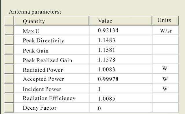
Figure 14. Antenna parameters as given by HFSS.
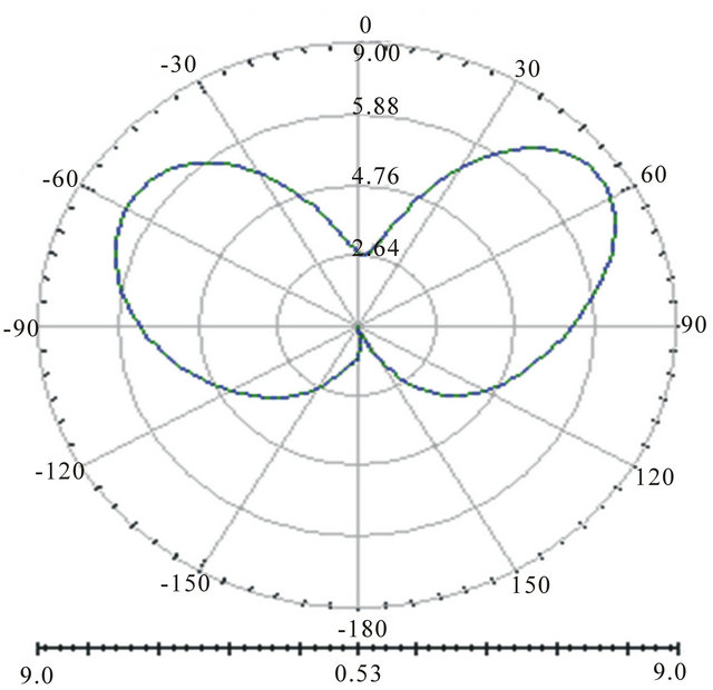
Figure 15. The E-field diagram pattern (for phi = 0 deg).

Figure 16. The E-field 3D polar diagram pattern.
Table 2. The impedances table in PCS band.

4. Conclusions
To design a PIFA for PCS band, we followed a methodology based on parametric simulations. During the design process, we can make some conclusions:
1) The PIFA characteristics are affected by each of the changed parameter (the height of the radiating plate, the ground plane dimensions, the position and width of the short plate, the position of the feeding point).
2) When we work in a medium bandwidth (like our case 140 MHz), any linear relation can’t be established between the way the characteristics of the antenna change and the way the parameter change. The parametric simulations are very interesting to make effective choice.
3) It’s interesting in the design of the PIFA to search an effective solution not the optimal one. In fact, difference will be very little, and also the values of the PIFA dimensions must be practical not theoretical. The important fact is that the solution respects the requirements.
4) In comparison with precedent designed PIFA [4,5] for different frequency bands, the antenna presents a very high radiation efficiency and larger bandwidth.
5) The designed PIFA for the PCS use respects the requirements especially for the resonant frequency, the VSWR, the bandwidth, the reflection loss, the anisotropy and the miniaturization.
The Table 3 summarizes the characteristics and dimensions of the designed antenna. The analysis of those
Table 3. The design antenna parameters and dimensions.
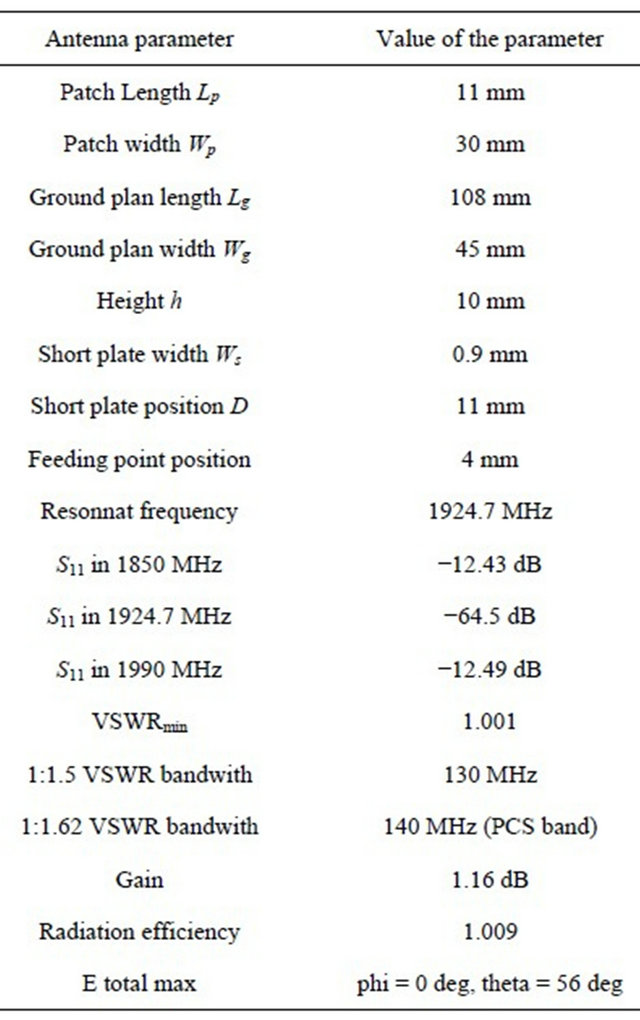
results makes from our designed antenna a succeeded trade-off that respects PCS requirements.
REFERENCES
- K. L. Wong, “Introduction and Overview,” In: K. L. Wong, Ed., Planar Antennas for Wireless Communications, John Willy and Sons, Hoboken, 2003, p. 1.
- K. L. Virga and Y. Rahmat-samii, “Low-Profile Enhanced Bandwith PIFA for Wireless Communications Packaging,” IEEE Transactions on Microwave Theory and Techniques, Vol. 45, No. 10, 1997, pp. 1879-1888. doi:10.1109/22.641786
- W.-J. Liao, T.-M. Liu and S.-Y. Ho, “Miniaturized PIFA Antenna for 2.4 GHz ISM Band Applications,” IEEE Proceedings of the 6th European Conference on Antennas and Propagation (EUCAP), Prague, 26-30 March 2012, pp. 3034-3037.
- A. K. Skrivervik, J.-F. Zürcher, O. Staub and J. R. Mosig, “PCS Antenna Design: The Challenge of Miniaturization,” IEEE Antennas and Propagation Magazine, Vol. 43, No. 4, 2001, pp. 12-27. doi:10.1109/74.951556
- Ansoft Corporation, “HFSS 10.0 User’s Guide,” Ansoft Corporation, Pittsburg, 2005.
- J. McClure, “Statistics for Microarrays: Design, Analysis, and Inference,” Rev.1.06, Ansoft Corporation, Pittsburg, 2005.