World Journal of Condensed Matter Physics
Vol.06 No.03(2016), Article ID:70063,8 pages
10.4236/wjcmp.2016.63024
Temperature Effect on Capacitance of a Silicon Solar Cell under Constant White Biased Light
Ibrahima Diatta1, Ibrahima Ly2, Mamadou Wade2, Marcel Sitor Diouf1, Senghane Mbodji3, Grégoire Sissoko1
1Physics Department, Faculty of Sciences and Techniques, University of Cheikh Anta Diop, Dakar, Senegal
2Electromechanical Engineering Department, Polytechnic School of Thies University, Thies, Senegal
3University of Alioune DIOP, Bambey, Senegal

Copyright © 2016 by authors and Scientific Research Publishing Inc.
This work is licensed under the Creative Commons Attribution International License (CC BY).
http://creativecommons.org/licenses/by/4.0/


Received 11 July 2016; accepted 22 August 2016; published 25 August 2016
ABSTRACT
In static regime with polychromatic illumination, using the expression of the solar cell capacitance to determine the silicon solar cell capacitance C0(T) in short-circuit, is the purpose of this article. The expression of the excess minority carries density δ(x) from the continuity equation. The expression of δ(x) is used to determine the photovoltage expression. The capacitance efficiency dependence on Xcc(T) is studied. Xcc(T) is the abscissa of the maximum of δ(x).
Keywords:
Solar Cell, Capacitance, Temperature

1. Introduction
The depletion region of a solar cell called transitional capacity due to ionization of fixed charges can be assimilated to a plane capacitor [1] . Recombination velocity at the junction which sets the operating point, the open circuit to short circuit [2] [3] determines the diffusion capacitance thickness. The latter is due to the diffusion of minority charge carriers [4] . From different regimes i.e. steady state [5] [6] , transient state [7] [8] or frequency dynamic [9] [10] , the solar cell can be studied.
The aim is to determine the doping rate [11] , and diffusion capacitance has been studied several times in static regime [12] [13] . The space charge region (SCR) expansion is also obtained under transient regime [14] . The excess minority carrier recombination parameters in the bulk and surface are detailed in frequency dynamic state [15] [16] . Electrical parameters [17] [18] : capacitance, inductance united to each solar cell area, the series and shunt resistors [19] [20] are also produced. Thus for separated areas of excitation frequencies of the solar cell, equivalent electrical models [21] are established. The temperature acts on the electrical parameters and the solar cell performance [22] . This influence is in the solar cell operating conditions in darkness or in light. Under static state and polychromatic illumination, by using the expression of solar cell capacitance, we determine in this work the capacitance C0(T) of a silicon solar cell in short circuit.
2. Theoretical Background
The solar cell is n + -p-p + type and its structure is shown in Figure 1.
When the solar cell is illuminated, there is creation of electron-hole pairs in the base. The excess minority carriers’ density in the base is modeled by the following continuity equation:
 (1)
(1)
with
δ(x) is the electrons density generated in the base at position x,
G(x) is the minority carriers generation rate at position x in the base [23] and given by
 (2)
(2)
Coefficients ai and bi are obtained from tabulated values of the radiation in A.M1, 5 condition [24] .
These coefficients are given as follow: a1 = 6.13 × 1020 cm−3/s; a2 = 0.54 × 1020 cm−3/s; a3 = 0.0991 × 1020 cm−3/s; b1 = 6630 cm−1; b2 = 1000 cm−1; b3 = 130 cm−1, L is the electron diffusion length in the base, and τ their lifetime. D(T) is the electron diffusion coefficient in the base given by the well known Einstein relation, temperature dependant, expressed as:
 (3)
(3)
and
 (4)
(4)
 is the mobility, [25] . Coefficient for electrons, given as:
 (5)
(5)
kb is the Boltzmann constant, q is the elementary charge of an electron Equation (1) has the general solution
 (6)
(6)
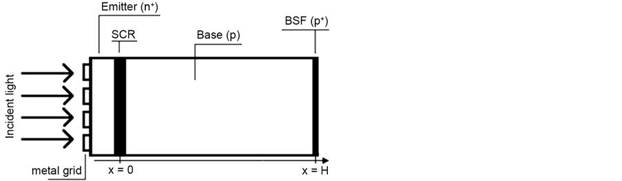
Figure 1. An n + -p-p + structure of a silicon solar cell.
Expressions of A and B are determined from the following boundary conditions [13] [14] :
1) At the junction (x = 0)
 (7)
(7)
2) At the back surface (x = H)
 (8)
(8)
Sf is the excess minority carriers recombination velocity at the junction, it also characterizes the operating point of the solar cell [3] [4] .
Sb is the recombination velocity on the back of excess charge minority carriers in the base [4] .
3. Excess Minority Carriers Density
3.1. The Effect of Temperature on the Minority Carriers Density
Figure 2 illustrates the minority charge carriers density when the solar cell is in short-circuit state in function of the depth in the base for different temperature values.
Three parts are noted in Figure 2.
The first part which is the negative gradient. This gradient corresponds to the passage of minority carriers created ted in this part. The second part represents a zero gradient. This gradient defines the point of maximum density corresponding to the abscissa Xsc(T). This gradient is a concentration of minority carriers. This gradient at this point defines the storage barrier of minority charge carriers. The third part corresponds to a negative gradient. This gradient prevents the minority carriers passage towards the barrier. These carriers will be recombined in volume and in solar cell back surface.
The variation of temperature is more sensitive at the maximum density point corresponding to the abscissa Xsc(T). The shift of the maximum in depth when the temperature rises, causes a space charge zone enlargement.
3.2. Operating Point Effect on Relative Minority Carriers Density
The minority carrier density profile in function of depth in the base is proposed in Figure 3 when the solar cell is in short circuit and in open circuit.
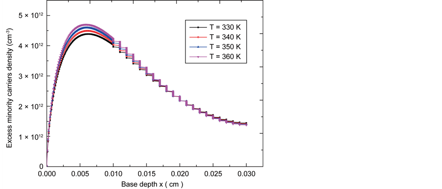
Figure 2. Minority carriers density versus base depth for different temperature values, Sf = 6 × 106 cm/s, in short-circuit operation.
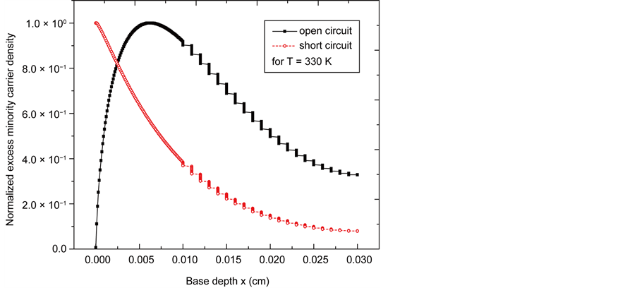
Figure 3. Normalized minority carriers density versus base depth.
Xoc(T) is the space charge zone thickness when the solar cell operates in open circuit.
Xsc(T) is the space charge zone thickness when the solar cell operates in short-circuits.
Then the solar cell capacitance efficiency η(T) can be defined from the Xoc(T) and Xsc(T) abscissae in the form [12] .
 (9)
(9)
The capacitance model study of a plane capacitor  can be done by comparing two relative density
maximum abscissae. Looking for the Performance capacitance simplifies to that of the Xsc(T) abscissa, because the value of Xoc(T) is negligibility compared to that of Xsc(T).
4. Photovoltage
The solar cell photovoltage is given by Boltzmann’s equation:
 (10)
(10)
where VT is the thermal voltage, it is given as follows:
 (11)
(11)
Nb is the doping rate and ni is the minority charge carriers intrinsic density [7] expressed as:
 (12)
(12)
Eg is the energy gap, it corresponds to the difference between the energy of the conduction band Ec and the valence band Eg. Eg = 1.12 × 1.6 × 10−19 J; A is a constant. A = 3.87 × 1016 cm−3∙K−3/2.
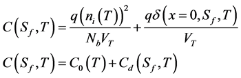
5. Capacitance
Using the photovoltage expression, the solar cell capacitance is obtained as:
 (13)
(13)
with
 (14)
(14)
and
 (15)
(15)
Equation (16) can be written as follows:
 (16)
(16)
Taking into account the photovoltage expression and the minority carrier density, we get the following relation:
 (18)
(18)
where
 (19)
(19)
 (20)
(20)
C0(T) is the solar cell capacitance when operating under short circuit.
Cd(T, Sf) is the solar cell diffusion capacitance at temperature T, at a given operating point represented by Sf.
Figure 4 shows the solar cell capacitance profile in function of the recombination velocity at the junction for different temperature values.
This curve (Figure 4) shows three levels and is decreasing:
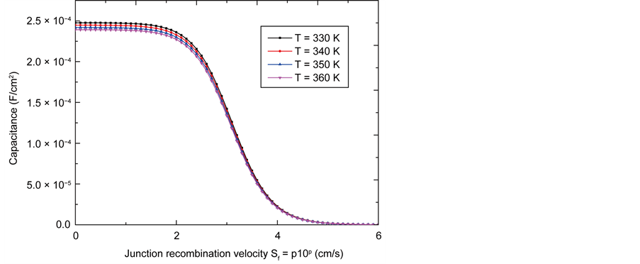
Figure 4. Capacitance versus junction recombination velocity.
1) The solar cell zone in open circuit, the recombination velocity is less than 2 × 102 cm/s. There is a stability and maximum capacitance. So there is storage of minority carriers in the emitter-base junction.
2) The solar cell zone in short circuit, the upper junction recombination velocity is 4 × 104 cm/s. low capacitance is reached. Then there is an important passage of minority charge carriers in the emitter-base junction.
The part between the open circuit and short circuit, the solar cell capacitance is decreasing. The latter is due to crossing of minority charge carriers in excess at the emitter-base junction.
When the solar cell is in open circuit (Sf < 2 × 102 cm∙s−1), the temperature influence is more visible. The diffusion capacitance comes a bit, it is the temperature that affect through C0(T). This capacitance C0(T) decreases as the temperature increases. Low capacitance causes the narrowing of its thickness. This shrinkage is due at the motion of short circuit operating point.
Influence of Temperature on the Solar Cell Capacitance in Short Circuit Operation
The Figure 5 shows the solar cell capacitance profile in short-circuiting in function of temperature.
In the limit of a minimum value Xsc(T) for abscissa Topt, the solar cell capacitance has a linear decrease with temperature. This reduction takes place at temperatures below Topt. The depletion zone extension is identical to the decreased of capacitance solar cell.
A large slope-related linear increases in capacitance. This increase occurs at temperatures higher than Topt. This increase corresponds to the narrowing of the thickness Xsc(T). The optimum temperature provides a high performance capacitance.
The projection of the two tangents meeting point to the curve on the temperature axis provides Topt Designing a solar cell capacitance theoretical model through the curve progression is given by [26] :
 (21)
(21)
with,
χ is determined from the intercept, it is equivalent to a capacitance,
γ is the slope with Tγ homogeneous to a capacitance.
Table 1 gives the values of χ and γ obtained from the curve of Figure 5.
The optimum temperature Topt = 362 K and the corresponding yield is η = 0.999.
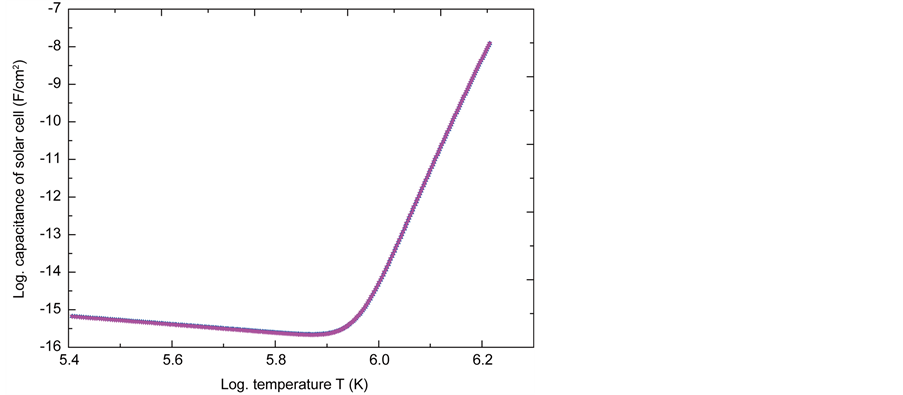
Figure 5. Capacitance versus temperature (Sf = 6 × 106 cm/s).

Table 1. Values of χ and γ in term of the temperature.
6. Conclusions
Capacitance efficiency dependence on Xsc(T) is shown in this study. Xsc(T) is the thickness of the solar cell space charge zone in short circuit. The explanation of the capacitance of the solar cell is used to determine the expression of C0(T) and Cd(T, Sf).
Optimum temperature Topt is defined by fluctuations of the solar cell capacitance in term of temperature. The optimum temperature provides a high performance capacitance. In the limit of a minimum value Xsc(T) for abscissa Topt, the solar cell capacitance has a linear decrease with temperature. This reduction takes place at temperatures below Topt. The space charge zone extension is identical to the solar cell capacitance decrease. However, the capacitance per unit length increase with temperature is observed. This increase occurs at temperatures higher than Topt. This increase corresponds to the Xsc narrowing.
Cite this paper
Ibrahima Diatta,Ibrahima Ly,Mamadou Wade,Marcel Sitor Diouf,Senghane Mbodji,Grégoire Sissoko, (2016) Temperature Effect on Capacitance of a Silicon Solar Cell under Constant White Biased Light. World Journal of Condensed Matter Physics,06,261-268. doi: 10.4236/wjcmp.2016.63024
References
- 1. Wang, C.H. and Neugroschel, A. (1987) Minority-Carrier Lifetime and Surface Recombination Velocity Measurement by Frequency-Domain Photpluminescence. IEEE Transaction on Electron Devices, 38, 2169-2180.
http://dx.doi.org/10.1109/16.83745 - 2. Ly Diallo, H., Wade, M., Idrissa, L., Diaye, N.M., Dieng, B., Lemrabott, O.H., Amadou, S.M. and Sissoko, G. (2012) 1D Modeling of a Bifacial Silicon Solar Cell under Frequency Modulation, Monochromatic Illumination: Determination of the Equivalent Electrical Circuit Related to the Surface Recombination Velocity Research. Journal of Applied Sciences, Engineering and Technology, 4, 1672-1676.
- 3. Bayhan, H. and Kavasglu, A.S. (2003) Admittance and Impedance Spectroscopy on Cu(In,Ga)Se2 Solar Cells. Turkish Journal of Physics, 27, 529-535.
- 4. Sahin, G., Dieng, M., El Moujtaba, M.A.O., Ibra Ngom, M., Thiam, A. and Sissoko, G. (2015) Capacitance of Vertical Parallel Junction Silicon Solar Cell under Monochromatic Modulated Illumination. Journal of Applied Mathematics and Physics, 3, 1536-1543.
http://dx.doi.org/10.4236/jamp.2015.311178
http://dx.doi.org/10.4236/jamp.2015.311178
http://www.scirp.org/journal/jamp
http://dx.doi.org/10.4236/jamp.2015.311178 - 5. Scofield, J.H. (1995) Effets of Series Resistance and Inductance on Solar Cell Admittance Measurements. Solar Energy Materials and Solar Cells, 37, 217-233.
http://dx.doi.org/10.1016/0927-0248(95)00016-X - 6. Kumar, R.A., Suresh, M.S. and Nagaraju, J. (2001) Measurement of AC Parameters of Gallium Arsenide (GaAs/Ge) Solar Cell by Impedance Spectroscopy. IEEE Transactions on Electron Devices, 48, 2177-2179.
http://dx.doi.org/10.1109/16.944213 - 7. Dieng, A., Zerbo, I., Wade, M., Maiga, A.S. and Sissoko, G. (2011) Three-Dimensional Study of a Polycrystal Line Silicon Solar Cell: The Influence of the Applied Magnetic Field on the Electrical Parameters. Semiconductor Science and Technology, 26, Article ID: 095023.
http://dx.doi.org/10.1088/0268-1242/26/9/095023 - 8. Zetterlund, B. and Steckl, A.J. (1991) Low-Temperature Operation of Silicon Surface Channel Charge Coupled Devices. IEEE Transactions on Electron Devices, 34, 39-51.
http://dx.doi.org/10.1109/T-ED.1987.22883 - 9. Furlan, J. and Amon, S. (1985) Approximation of the Carrier Generation Rate in Illuminated Silicon. Solid-State Electronics, 28, 1241-1243.
http://dx.doi.org/10.1016/0038-1101(85)90048-6 - 10. Mohammad, S.N. (1987) An Alternative Method for the Performance Analysis of Silicon Solar Cells. Journal of Applied Physics, 61, 767-777.
http://dx.doi.org/10.1063/1.338230 - 11. Kunst, M. and Sanders, A. (1992) Transport of Excess Carriers in Silicon Wafers. Semiconductor Science and Technology, 7, 51-59.
http://dx.doi.org/10.1088/0268-1242/7/1/009 - 12. Diatta, I., Diagne, I., Sarr, C., Faye, K., Ndiaye, M. and Sissoko, G. (2015) Silicon Solar Cell Capacitance: Influence of both Temperature and Wavelength. IPASJ International Journal of Computer Science (IIJCS), 3, 1-8.
http://www.ipasj.org/IIJCS/IIJCS.htm - 13. Liou, J.J., Lindholm, F.A. and Malocha, D.C. (1988) Forward-Voltage Capacitance of Heterojunction Space Charge Regions. Journal of Applied Physics, 63, 5015.
http://dx.doi.org/10.1063/1.340448 - 14. Mbodji, S., Mbow, B., Barro, F.I. and Sissoko, G. (2011) A 3D Model for Thickness and Diffusion Capacitance of Emitter-Base Junction Determination in a Bifacial Polycrystalline Solar Cell under Real Operating Condition. Turkish Journal of Physics, 35, 281-291.
- 15. Yaron, G. and Bentchkowsky, D.F. (1980) Capacitance Voltage Characterization of Poly Si-SiO2-Si Structures. Solid-State Electronics, 23, 433-439.
http://dx.doi.org/10.1016/0038-1101(80)90078-7 - 16. Jakubowski, A. (1981) Graphic Method of Substrate Doping Determination from C-V Characteristics of MIS Capacitors. Solid-State Electronics, 24, 985-987.
http://dx.doi.org/10.1016/0038-1101(81)90123-4 - 17. Ndiaye, El H., Sahin, G., Dieng, M., Thiam, A., Ly Diallo, H., Ndiaye, M. and Sissoko, G. (2015) Study of the Intrinsic Recombination Velocity at the Junction of Silicon Solar Cell under Frequency Modulation and Radiation. Journal of Applied Mathematics and Physics, 3, 1522-1535.
http://dx.doi.org/10.4236/jamp.2015.311177 - 18. Diao, A., Thiam, N., Zoungrana, M., Ndiaye, M., Sahin, G. and Sissoko, G. (2014) Diffusion Coefficient in Silicon Solar Cell with Applied Magnetic Field and under Frequency: Electric Equivalent Circuits. World Journal of Condensed Matter Physics, 4, 1-9.
http://dx.doi.org/10.4236/wjcmp.2014.42013 - 19. Corréa, A., Gaye, I., Ba, B., Ndiaye, A.L. and Sissoko, G. (1994) Solar Cells Parameters Determination by Constant Illumination Induced Transient Voltage Decay Method. Renewable Energy, 5, 166-168.
http://dx.doi.org/10.1016/0960-1481(94)90366-2 - 20. Thurmond, C.D. (1975) The Standard Thermodynamic Functions for the Formation of Electron and Hole in Ge, Si, GaAs and GaP. Journal of the Electrochemical Society, 122, 133-141.
http://dx.doi.org/10.1149/1.2134410 - 21. Sissoko, G., Nanéma, E., Corréa, A., Biteye, P.M., Adj, M. and Ndiaye, A.L. (1998) Silicon Solar Cell Recombination Parameters Determination Using the Illuminated I-V Characteristic. Renewable Energy, 3, 1848-1851.
- 22. Sissoko, G., Nanéma, E., Ndiaye, A.L., Bocandé, Y.L.B. and Adj, M. (1996) Minority Carrier Diffusion Length Measurement in Silicon Solar Cell under Constant White Bias Light. Renewable Energy, 3, 1594-1597.
- 23. Sissoko, G., Dieng, B., Corréa, A., Adj, M. and Azilinon, D. (2004) Silicon Solar Cell Space Charge Region Width Determination by a Study in Modeling. Renewable Energy, 3, 1852-1855.
- 24. Diallo, H.L., Amadou, S.M., Wereme, A. and Sissoko, G. (2008) New Approach of Both Junction and Back Surface Recombination Velocities in a 3D Modelling Study of a Polycrystalline Silicon Solar Cell. European Physical Journal Applied Physics, 42, 203-211.
http://dx.doi.org/10.1051/epjap:2008085 - 25. Sissoko, G., Sivoththanam, S., Rodot, M. and Mialhe, P. (1992) Constant Illumination-Induced Open Circuit Voltage Decay (CIOCVD) Method, as Applied to High Efficiency Si Solar Cells for Bulk and Back Surface Characterization. 11th European Photovoltaic Solar Energy Conference and Exhibition, Monteux, 12-16 October 1992, 352-354.
- 26. Chawla, B.R. and Gummel, H.K. (1971) Transition Region. Capacitance of Diffusion p-n Junction. IEEE Transactions on. Electron Devices, 18, 178-195.
http://dx.doi.org/10.1109/T-ED.1971.17172