Journal of Sensor Technology
Vol.2 No.3(2012), Article ID:22873,10 pages DOI:10.4236/jst.2012.23020
Morphology and Electrochemical Properties of Activated and Sputtered Iridium Oxide Films for Functional Electrostimulation*
1Department of Electrical and Computer Engineering, University of Utah, Salt Lake City, USA
2Blackrock Microsystems, Salt Lake City, USA
Email: #s.negi@utah.edu
Received June 3, 2012; revised July 5, 2012; accepted August 7, 2012
Keywords: Neural Prostheses; Electrode Stimulation; Charge Injection Capacity; Iridium Oxide
ABSTRACT
Iridium oxide (IrOx) has attracted much attention for neural interface applications due to its ability to transfer between ionic and electronic current and to resist corrosion. The physical, mechanical, chemical, electrical and optical properties of thin films depend on the method and parameters used to deposit the films. In this report, the surface morphology, impedance and charge capacity of activated iridium oxide film (AIROF) and sputtered iridium oxide film (SIROF) were investigated in vitro and compared. The Utah Electrode Array (UEA) having similar electrode area and shape were employed in this study. The electrode coated with AIROF and SIROF were characterized by scanning electron microcopy, cyclic voltammetry, electrochemical impedance spectroscopy and potential transient measurements to measure charge injection capacity (CIC). SIROF and AIROF selectively deposited on electrode tip had dendrite and granular microstructure, respectively. The CIC of unbiased SIROF and AIROF was found to be 2 and 1 mC/cm2, respectively, which is comparable to other published values. The average impedance, at a frequency of 1 kHz was ~65 and ~7 kΩ for the AIROF and SIROF, respectively. Low impedance and high CIC makes SIROF highly recommended stimulation and recording material.
1. Introduction
Functional electrical stimulation of the nervous system is a promising technique for the restoration of a variety of physiological functions, including controllable limb movement, hearing, and perhaps in longer-term, vision [1,2]. The artificial stimulation of living tissue requires a transfer of an electrical signal from an implantable microelectrode across the cell membrane of the neurons. A major factor limiting the widespread application of functional electrical stimulation has been the lack of stimulating electrodes that can be used for long-term, precise, are multipoint stimulation of the central or peripheral nervous system. The development of stimulating electrodes requires the ability to inject sufficient charge to evoke a response and induce minimal tissue damage at the stimulation site. Electrode materials with higher charge injection capacity (CIC) are desired to allow smaller electrodes. Small electrodes achieve higher stimulation current density while operating within safe voltage limits that avoid gas evolution by electrolysis or electrochemical reactions. Furthermore, higher CIC of electrode material lowers the potential required for stimulation, which could reduce injury at the stimulation site.
The miniaturization of the stimulating electrodes improves the spatial resolution and selectivity (ability to activate one population of neurons without activating neighboring populations). However, charge injection decreases as the area of the electrode decreases increasing the electrode impedance, which is not desired. Therefore, a large active area must be generated without increasing the geometrical surface area of the electrode. This can be achieved by tailoring the electrode surface morphology to generate high surfaces area films. Making the electrode material rough increases the real surface area (RSA) of the electrode, without altering the geometrical surface area (GSA). At the same time it should be noted that high frequency current pulse is employed for neural stimulation, at which the electrode charge capacity is only partly accessible due to the limit of diffusion rate of charge carriers in the solution. Hence, optimum roughness is desired. The physical (roughness etc.), electrical, chemical, mechanical and optical characteristics of thin films depend on the underlying substrate, the method of deposition, and deposition parameters. Different deposition methods and parameters yield different degrees of porosity, roughness and thickness which in turn affect film properties [3-9].
Iridium oxide (IrOx) has received considerable attention for electrical stimulation in biomedical applications due to its ability to inject charge [10,11] and corrosion resistant [12], and also in electronic displays due to its electrocatalytic [13] and electrochromic capabilities [14,15]. IrOx is highly conductive oxides having a bulk resistivity ranging from 30 to 100 μΩ-cm, at room temperature [9, 16]. Although it is generally agreed that the oxidation state of the Ir shifts between Ir3+ and Ir4+ as an electrochemical reaction [15], the exact nature of this redox reaction is still unclear.
The properties of the IrOx films depends on the structure, composition and morphology of the oxide film, which, in turn, depends on the condition and method used to deposit films. In this report, an in vitro comparison of the electrical properties of sputtered iridium oxide film (SIROF) and activated iridium oxide film (AIROF) is reported. Ir (to form AIROF) and SIROF are deposited on the Utah Electrode Array (UEA). AIROF and SIROF surface and electrochemical properties are measured and compared with each other for the suitability of these films as an electrode material for neuroprostheses applications.
2. Materials and Methods
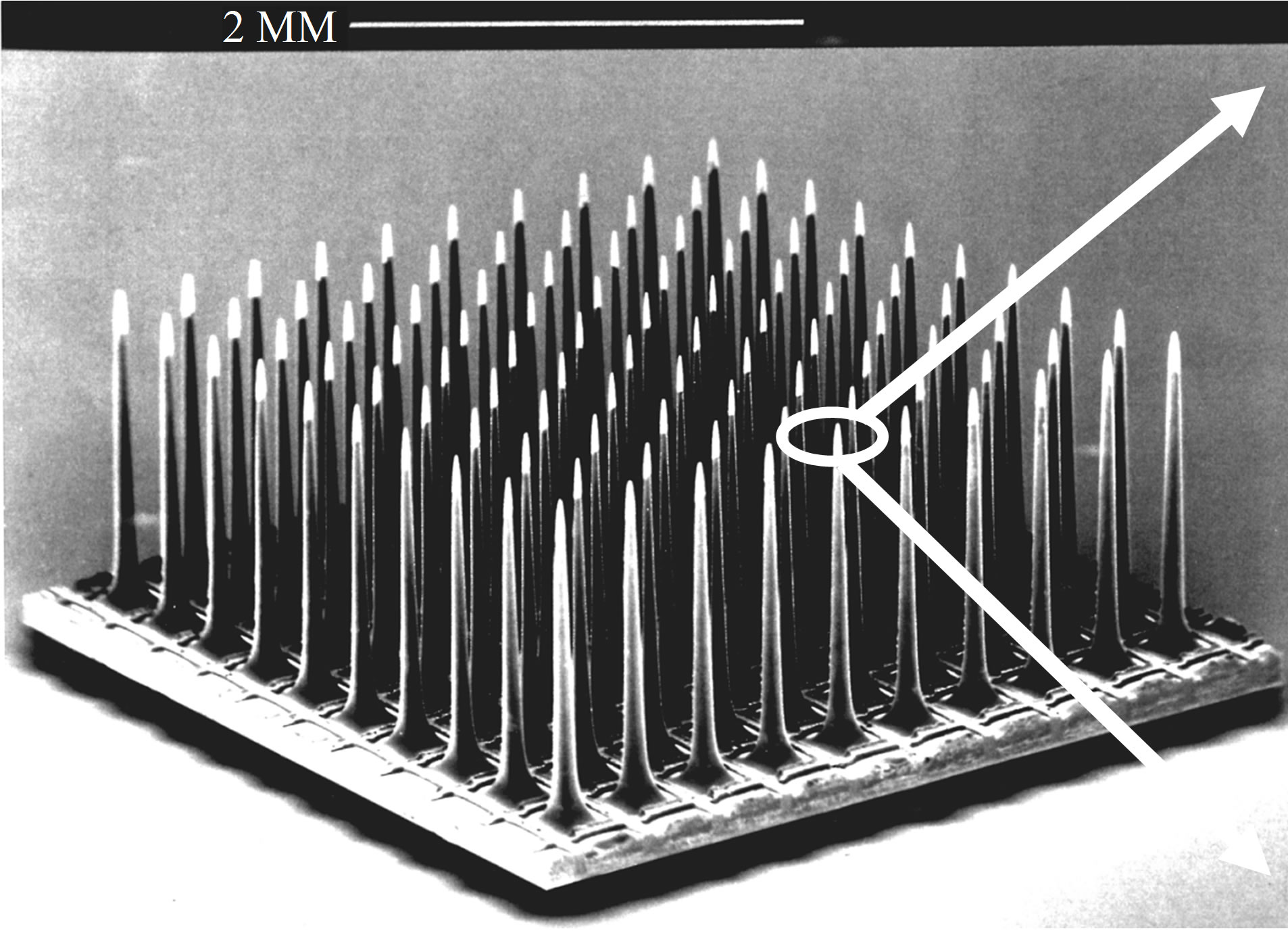
SIROF and AIROF were deposited on the Utah Electrode Array (UEA). Scanning electron micrograph of the UEA is shown in Figure 1(a). The length of the de-insulated (exposed) electrode tip or tip exposure typically ranges from 20 to 100 μm (Figure 1(b)). A detailed description of the UEA fabrication is given elsewhere [17,18]. All the thin films were deposited in a TM Vacuum SS-40C-IV multi cathode sputtering system. Prior to any deposition, the load lock chamber was evacuated to 2 × 10⁻⁷ Torr using first a mechanical and then a cryogenic pump. Ar and O2 are supplied to the chamber via mass flow controllers. Titanium (Ti) was deposited on the electrode tips of the UEA before iridium (for AIROF) or IrOx (SIROF) deposition. Ti acts as an adhesive layer and was deposited using DC sputtering. The Ti layer was sputtered in Ar ambient at a chamber pressure of 10 m Torr with Ar flowing at 150 sccm (standard cubic centimeters per minute) and sputtering power of 90 W for 5 min. The sputtering parameters were optimized to achieve low stress Ti film. Ti target was 99.6% pure, 3 inches in diameter and 0.125 inches in thickness (Kurt J. Lesker). The deposition rate of Ti was 10 nm/min.
 (a)
(a)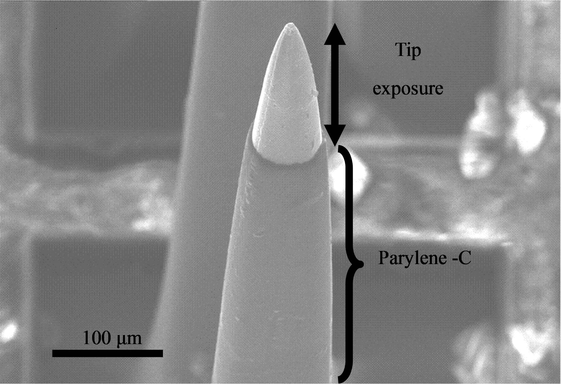 (b)
(b)
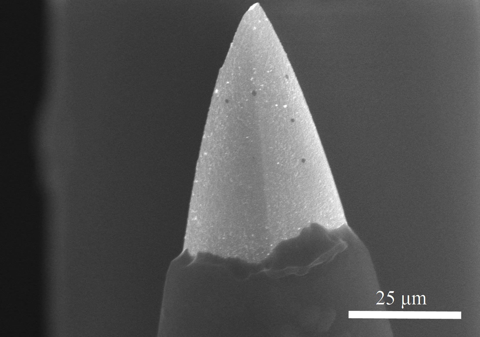
Figure 1. Scanning electron micrograph of the Utah Electrode Array (UEA), showing (a) the entire array and (b) a view of one electrode at higher magnification to show the tip exposure. The UEA is encapsulated by an insulating Parylene-C layer, with exception of the tip (~100 μm) of the electrode which forms the active site for stimulation or recording of neural signals.
SIROF was deposited by pulsed DC sputtering. The Ir target was 99.8% pure, 3 inch in diameter and 0.125 inches in thickness (Kurt J. Lesker, Pittsburgh, PA). The SIROF was reactively sputtered in Ar and O2 plasma with both gases flowing at the rate of 100 sccm. All the films were deposited at 10 mTorr using 100 W power for 20 min at pulse width 2016 ns. The pulse frequency was 100 kHz and deposition rate was 9.8 nm/min.
All the AIROF arrays were first DC sputtered with Ir. A process pressure of 20 mTorr was achieved using the throttle valve and an Ar gas flow rate of 150 sccm. The sputtering power was 90 W and deposition time was 12 minutes. The deposition rate of Ir was 16.3 nm/min. Ir electrodes were activated to form AIROF by potentiodynamic pulsing between –0.6 V and 0.8 V at 1 Hz in phosphate buffered saline (PBS) solution.
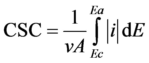
The film thicknesses were measured with a Tencor P-10 profilometer on a silicon witness wafer masked to yield a step. The surface morphology of SIROF and AIROF (after activation) and length of tip exposure were examined by scanning electron microscopy (SEM) using an FEI Nova NanoSEM microscope. Cyclic voltammetry (CV) and potential transient responses during current pulsing was measured in a three electrode cell comprising of Ag/AgCl as reference electrode, a large area Pt wire as a counter electrode and UEA electrodes as working electrode. All potentials were measured with respect to the reference electrode. CV data was acquired in a physiological PBS solution at room temperature in a commercial electrochemical test system (Gamry Instruments (PC4 potentiostat), Warminster, PA). The cyclic voltammograms was recorded at a 50 mV/s sweep rate between potential limits of –0.6 V and 0.8 V, beginning at the open circuit potential and sweeping in the positive direction first. The charge storage capacity (CSC) was calculated using following equation [19]
 (C/cm2) (1)
where, E is the electrode potential (V vs SSE), i is the measured current (AMP), Ea and Ec are the anodic and cathodic potential limits (V), respectively, A is the surface area of the exposed tip (cm2) and ν is the scan rate.
For CIC measurement, current pulsing was performed with STG 2008 stimulus generator (Multi Channel Systems MCS GmbH, Germany). Current pulses were delivered as charge-balanced biphasic pairs, cathodal first, with equal times and current amplitude for each phase. The pulse frequency was kept constant at 50 Hz, allowing ~19 ms between pulses. The cathodal pulse width of 0.2 was used to compare the CIC of unbiased SIROF and AIROF coated UEA. The potential transient was recorded with an oscilloscope and the maximum negative potential excursion (Emc) was calculated by subtracting the access voltage (Va), associated with ohmic resistance, from the maximum negative voltage in the transient. Emc is also equal to the potential immediately after the end of the cathodic pulse when Va is zero, as illustrated in Figure 2. Vd denotes the driving voltage which is maximum voltage required to deliver the current pulse. The maximum CIC of the SIROF and AIROF was defined at which the potential (Emc) reaches water reduction potential (–0.6 V).
Electrochemical impedance spectroscopy (EIS) was performed in the same Gamry test system used to record the CV. The applied sinusoidal bias had amplitude of 10 mV and measured impedance (Z) for frequencies from 1 Hz to 100 kHz. The electrode impedance was also measured with ZM3, an instrument to measure electrode impedance (Cyberkinetics Neurotechnology Systems Inc (CKI), Salt Lake City, Utah).
3. Results and Discussion
3.1. Surface Morphology
The thickness of Ti layer was 50 nm for each sample. The thickness of the IrOx and Ir samples measured on witness wafer was 195 nm and 190 nm, respectively. It should be noted that the thickness of sputtered films may differ when deposited on the electrode tip compared to the layers deposited on the witness wafer, due to the nonplanar geometry of the UEA. This geometry alters the angle and distance of the sputtered flux arriving at the tip surface. However, Ir and IrOx film thicknesses are comparable on the witness wafer and it will transform to comparable thicknesses on the electrode tips too, but not
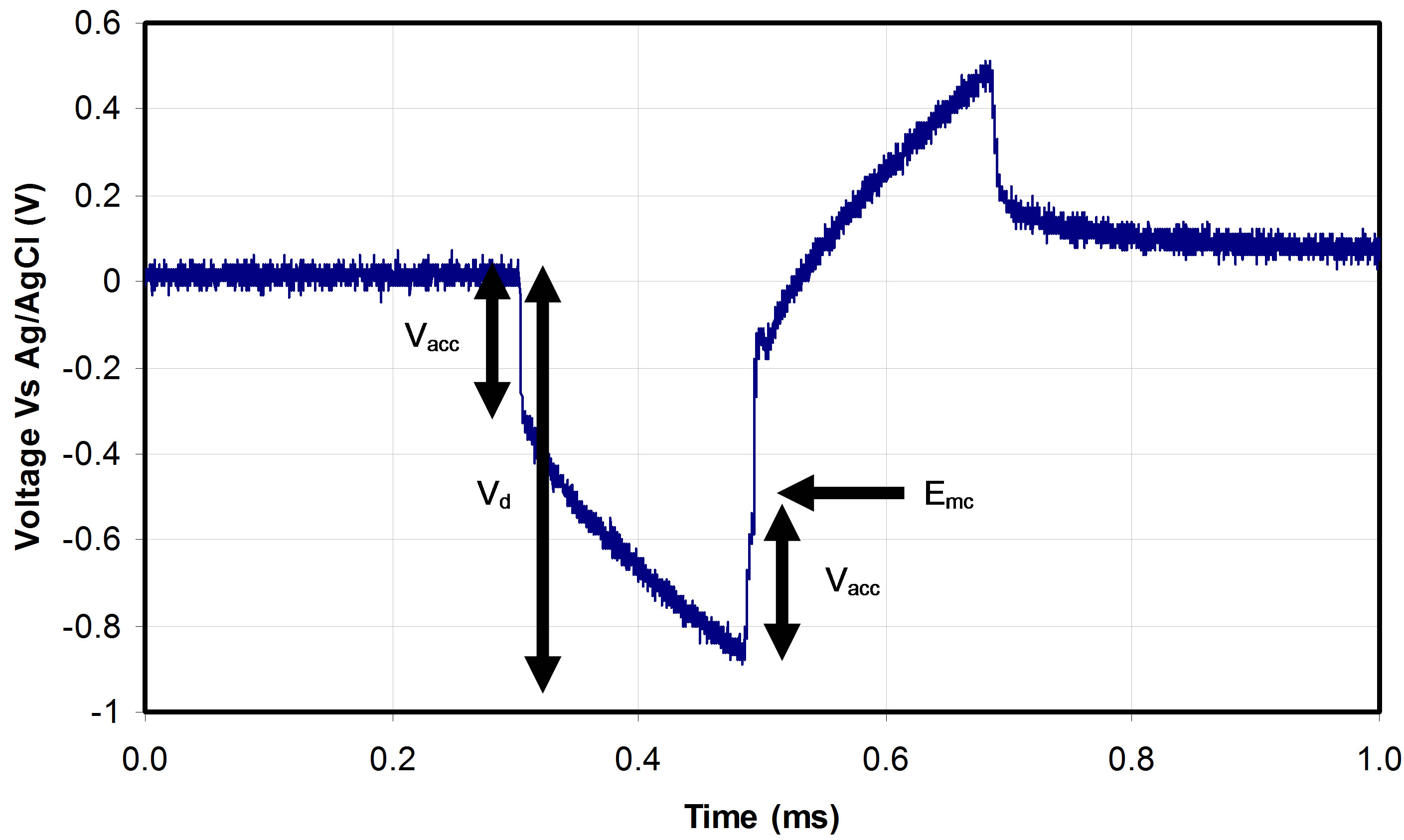
Figure 2. Representative voltage transient of an AIROF coated electrode of the UEA in which biphasic, symmetrical current pulse was passed at 50 Hz. The figure highlights maximum cathodic potential (Emc = –0.55 V) during a pulse.
identical to witness wafers.
Figure 3 illustrates scanning electron micrographs of electrode tips which were coated with SIROF and AIROF; (a), (c) and (e) are SEM micrographs of SIROF coated electrodes while (b), (d) and (f) are of AIROF coated electrodes at different horizontal field width (HFW). As seen in the highest magnification micrographs, SIROF have dendritic morphology while AIROF have granular morphology. The dendritic morphology of SIROF appears mechanically fragile compared to granular morphology of AIROF, considering the UEA will be implanted in to neural tissue with a high velocity pneumatic inserter. SIROF and AIROF coated UEA were inspected in SEM and impedance was measured in PBS solution, pre and post implantations (5 times) in the sciatic nerve of a cat. No delamination or visual defects in
 (a)
(a)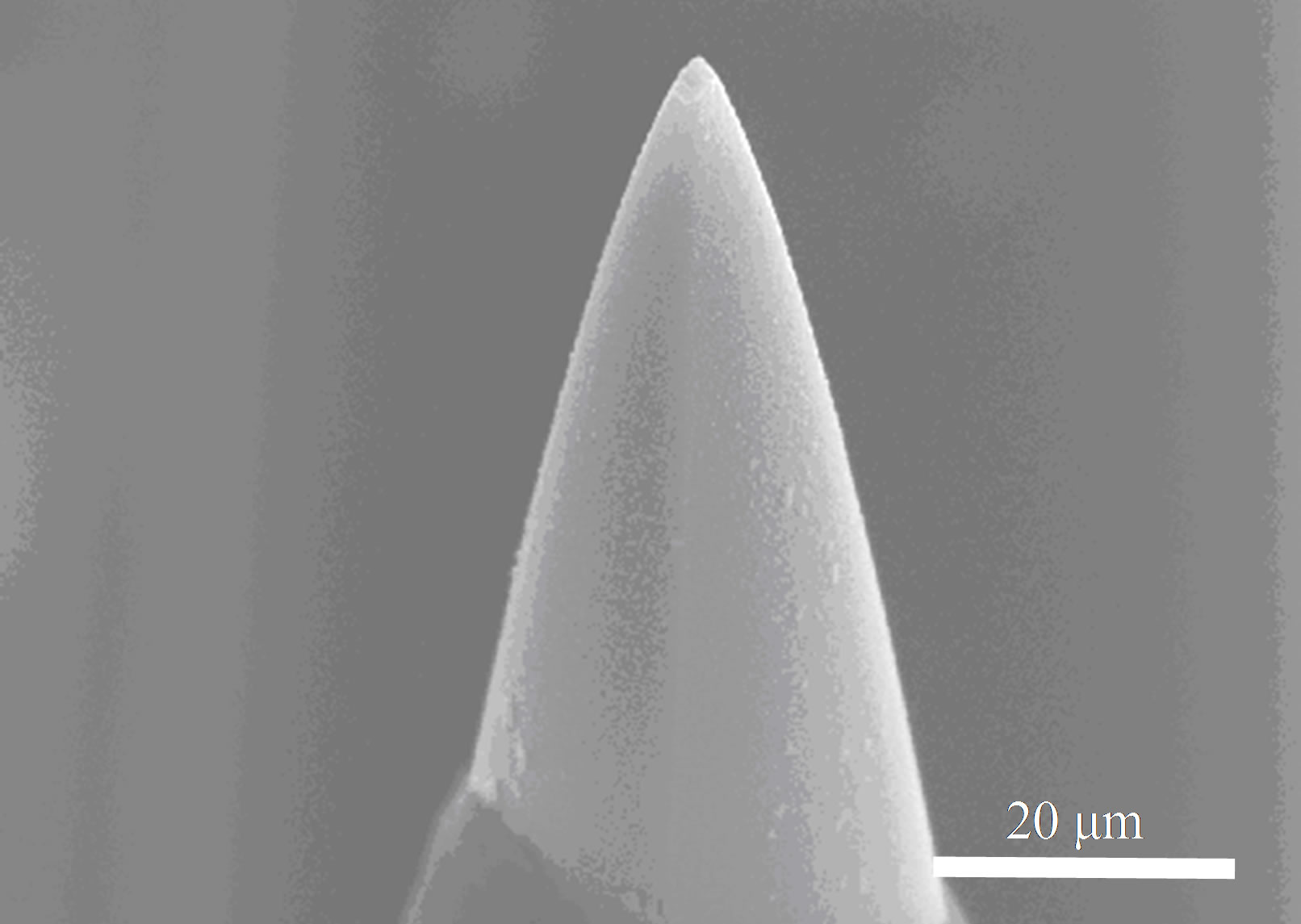 (b)
(b)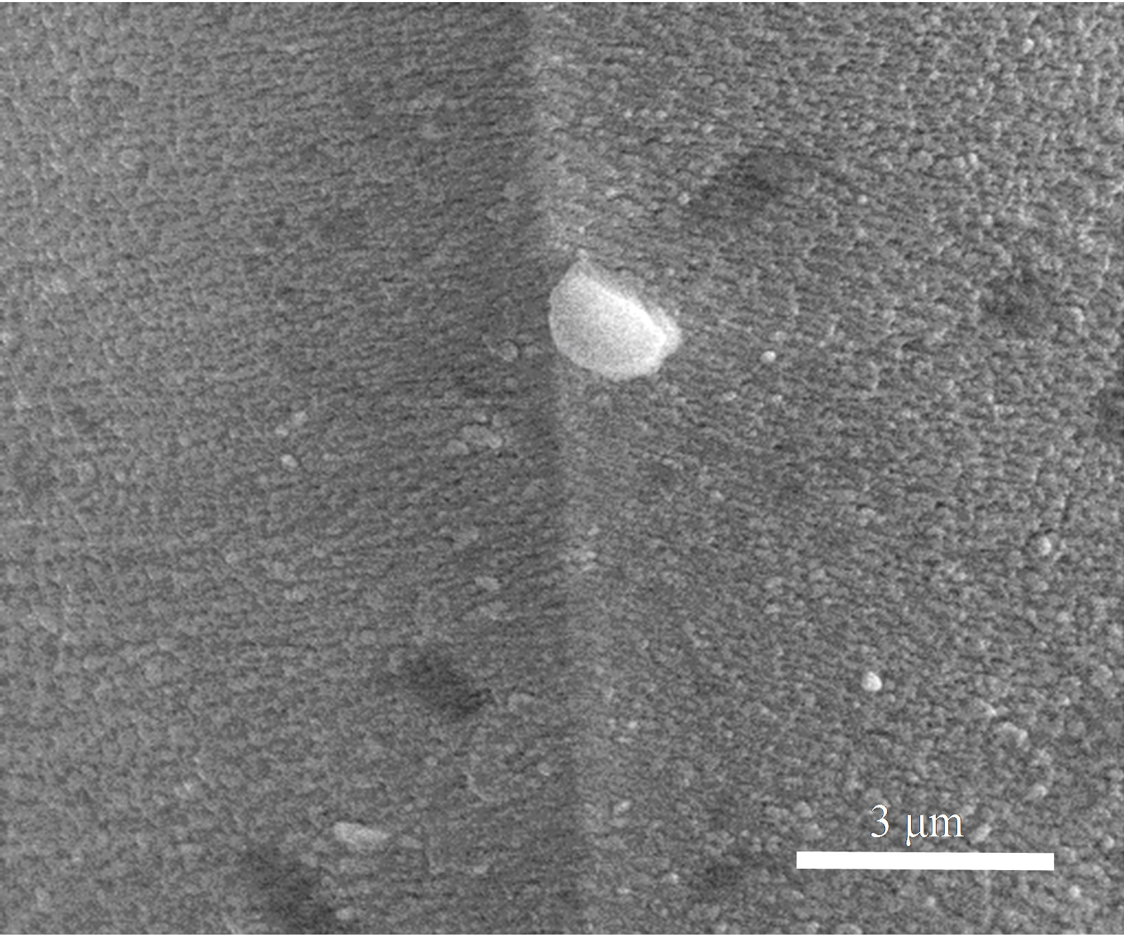 (c)
(c)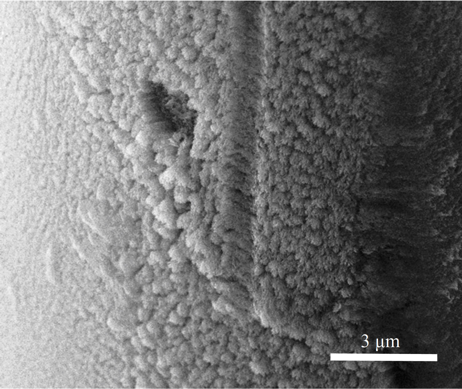 (d)
(d)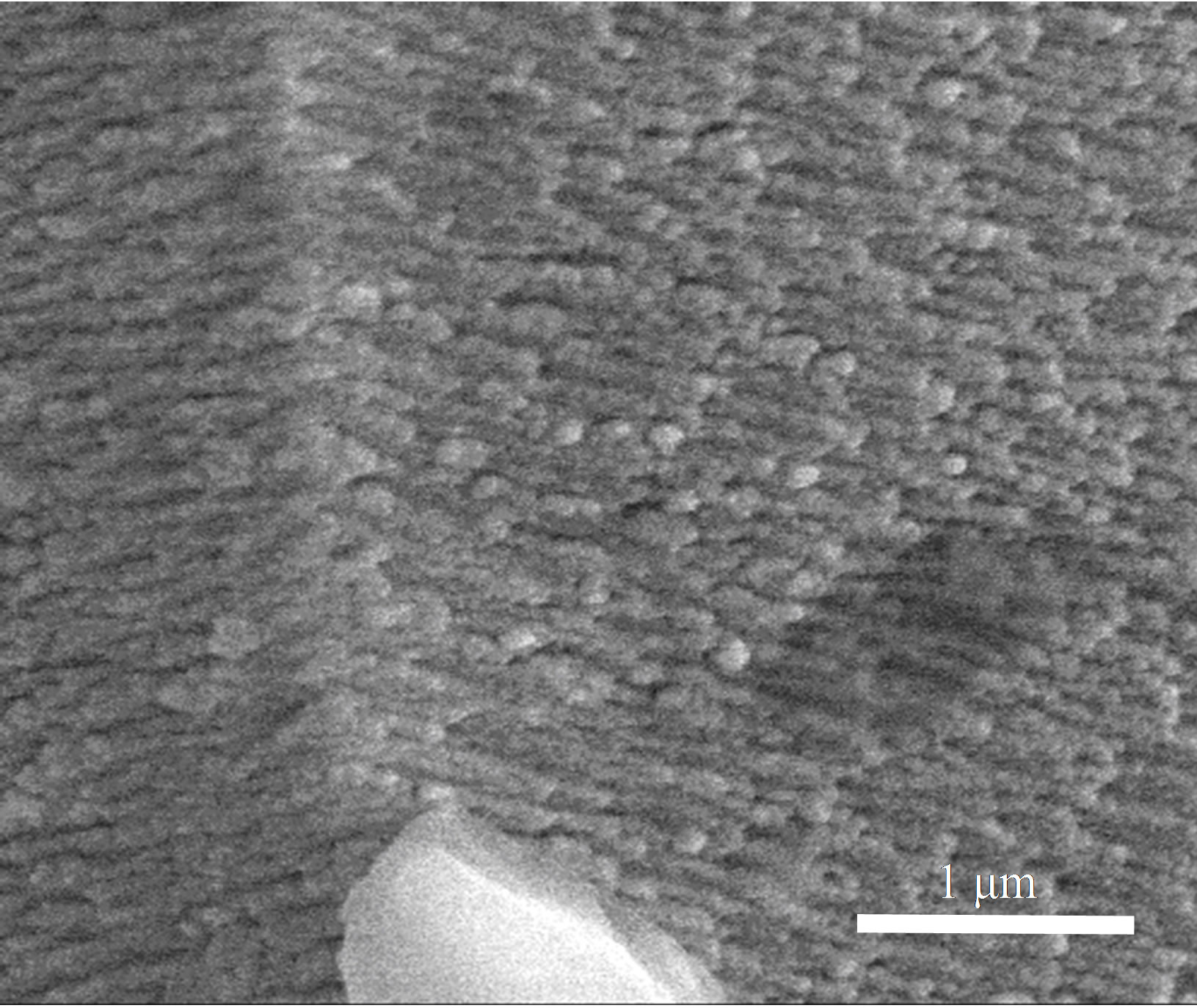 (e)
(e)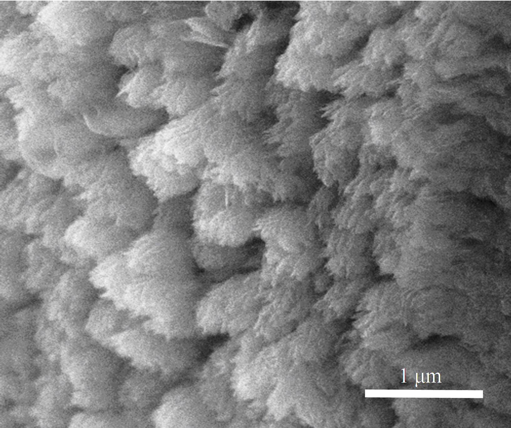 (f)
(f)
Figure 3. SEM micrographs of the SIROF (a), (c) and (e) and AIROF (b), (d) and (f) at different horizontal field width. SIROF has dendritic morphology while AIROF has granular morphology.
the SEM micrographs or significant change in impedance of SIROF and AIROF electrodes were observed indicating, not only, good adhesion of the films to the substrate, but also, good mechanical strength of the films.
3.2. Reliability/Soak Test of the SIROF and AIROF Coated UEA
In vitro testing was done to evaluate the stability of the arrays in PBS solution over time by monitoring electrode impedance. The impedance was measured with a ZM3 impedance meter (CKI). Figure 4 shows the impedance at 1 kHz of AIROF and SIROF coated arrays over a 3- month period. The median impedance of the AIROF electrodes before activation was 81.6 kΩ at 1 kHz and decreases to 64.8 kΩ at 1 kHz after activation and remained stable for the remaining 50 days. SIROF arrays were stable for over 90 days and their median impedance at 1 kHz was ~6.7 kΩ. The impedance of all the arrays were stable for over 3 months which suggests there was no encapsulation or device failure during the time tested.
3.3. Geometrical Surface Area Calculation
The surface area of electrode tip was used in determining the electrical characteristics of the electrodes, such as CIC, and charge storage capacity (CSC). The SEM micrographs in Figure 3(a)-(f) clearly indicate both the SIROF and AIROF have significant surface roughness, and therefore will have higher RSA. However, RSA is difficult to measure due to film surface roughness and porosity. The GSA of the UEA electrode tip was calculated by assuming the tip to be a cone. The GSA of cone, excluding the base of the cone is given by following equation,
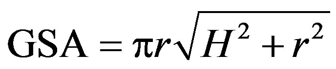 (2)
(2)
where, r is the radius of the base of the cone, and H is the length of the cone from the vertex to the center of the base. The tip exposure (H) and radius of the base of tip exposure (r) were measured by SEM. The GSA of the electrode tips were found to be ranging from 3.5 to 180 × 10–6 cm2.
3.4. Electrochemical Characterization
Bode plots of SIROF and AIROF coated electrodes of identical GSA (tip exposure of ~50 μm) are illustrated in Figure 5. For both SIROF and AIROF, the impedance amplitude at the higher frequency range was nearly independent of frequency and became frequency dependent at lower frequency. The frequency dependent impedance amplitude indicates capacitive charging as the dominant current flow mechanism. At frequencies below 104 Hz the impedance of SIROF was significantly lower than that of AIROF. At higher frequency (greater than 104 Hz), the impedance is attributed to the PBS solution, only [20]. Over a frequency range of 103 - 104 Hz, the AIROF electrode exhibits predominantly capacitive phase angle (–70˚), while SIROF electrodes has a more resistive phase angle (–10˚ to –20˚). There is significant impedance difference between the two, at frequencies relevant to neural stimulation (10 to 105 Hz).
The equivalent circuit model of the electrodeelectrolyte interface is shown in Figure 6, where Re is the electrolyte resistance, RCT is the charge transfer resistance and CPE is the constant phase element. Due to the nonideal capacitance response, CPE was used instead of ideal capacitor. The CPE impedance is given by
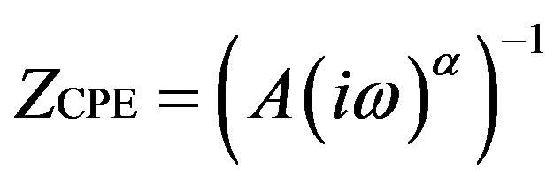
where, ω is the angular frequency, A and α are fre-
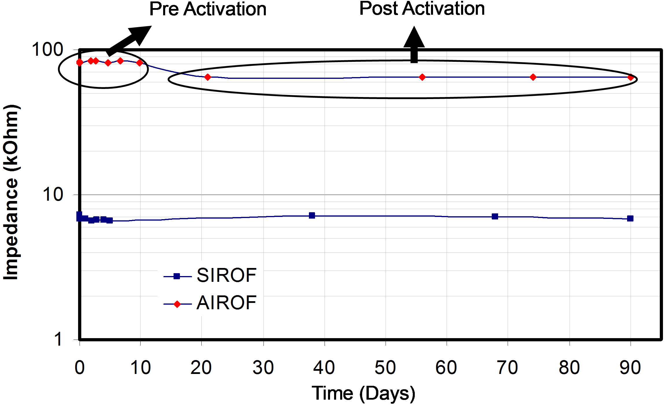
Figure 4. The stability of the AIROF and SIROF coated electrodes in vitro was investigated measured for 3 months using impedance spectroscopy. The median impedance of SIROF coated electrode array was stable at 6.7 ± 3 kΩ at 1 kHz. The activation to form AIROF was done on 20th day which brought the median impedance of the array from 81.6 to 64.8 ± 10 kΩ at 1 kHz.
quency-independent parameters, and 0 ≤ α ≥ 1. Note that CPE describes an ideal capacitor for α = 1 (A being capacitance) and an ideal resistor for α = 0. Simulated spectra using fit parameters are shown in Figure 7 while the fitting parameters are given in Table 1. The capacitance and resistance of SIROF coated UEA is significantly lower than that of AIROF. The surface roughness given by α and fitting data suggest that AIROF was rougher than SIROF. The cut-off frequency of the SIROF and AIROF coated electrodes calculated from Bode plots were estimated to be 200 Hz and 10 kHz respectively. The higher cut-off frequency of AIROF can be associated to a higher resistivity of the film and to the enhanced anodic potential of the Ir4/Ir3 system. The higher resistivity may be attributed to the porosity of the film due to significant increase in electron scattering from the surface of the film [14]. The neural signal frequency is in the range of few kHz.
Furthermore, thermal (Johnson) noise should be low for recording neural signals. Johnson noise for SIROF and AIROF coated UEA was calculated using equation , where, k is Boltzmann constant, T is temperature, R is electrode resistance, and B is noise
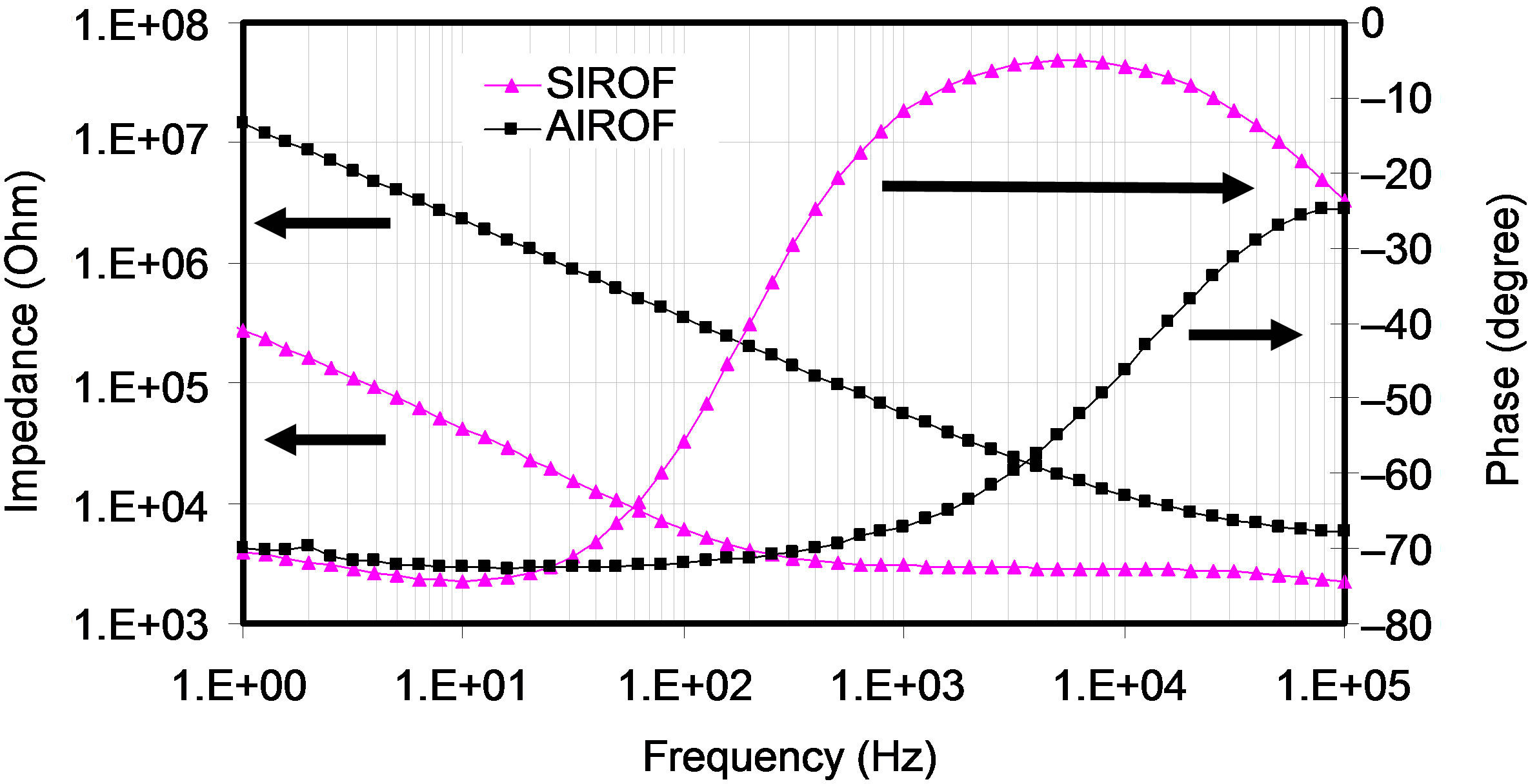
Figure 5. Bode plot presents the electrode impedance as a function of frequency of the SIROF and AIROF coated electrodes of the UEA. The impedance of the SIROF is lower than that of AIROF especially at frequency less than or equal to 1 kHz.
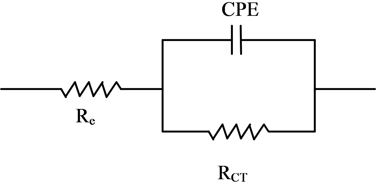
Figure 6. Equivalent circuit of the electrode-electrolyte systems.
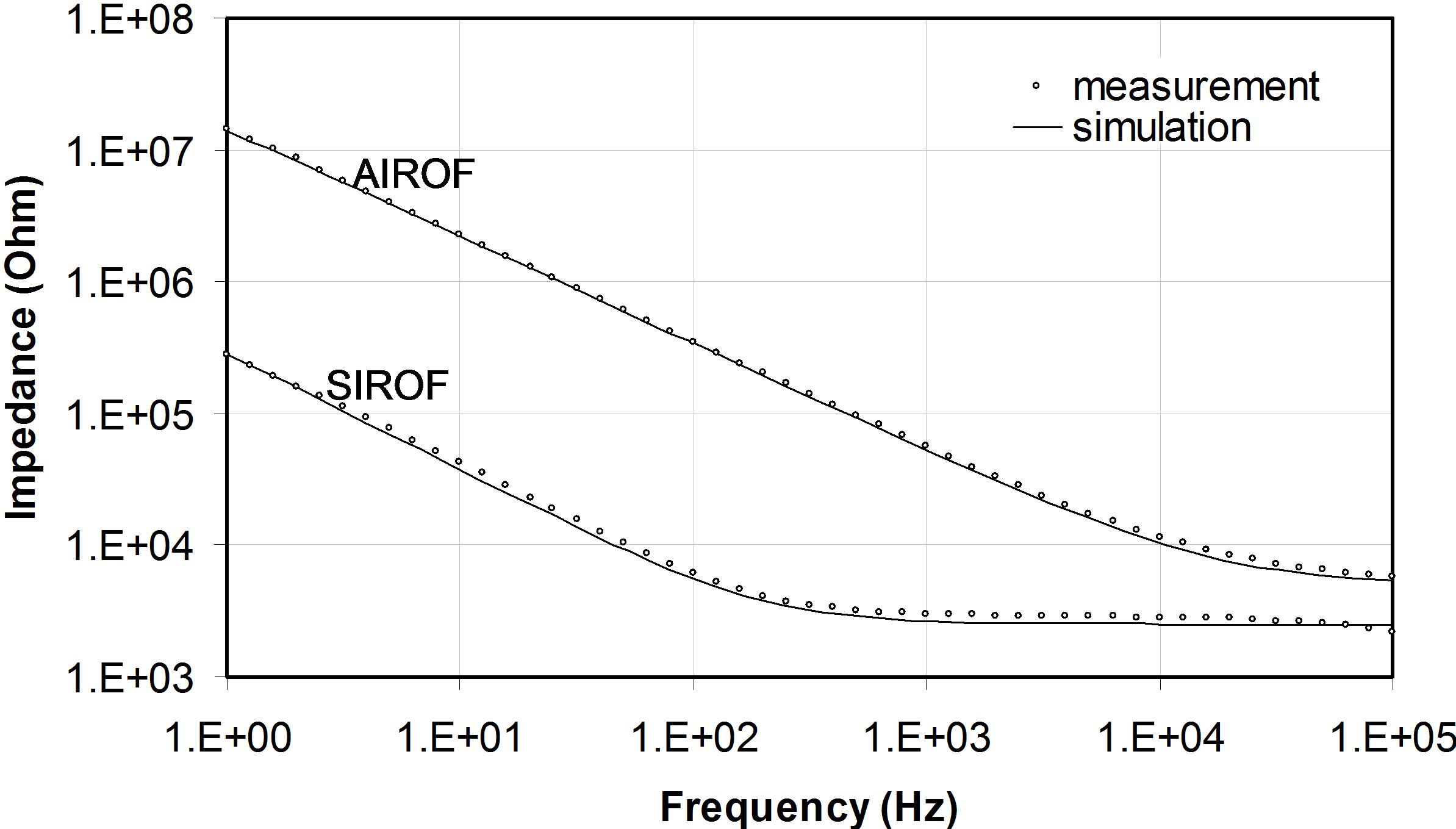
Figure 7. Bode plot of SIROF and AIROF coated UEA with measured and simulation data.
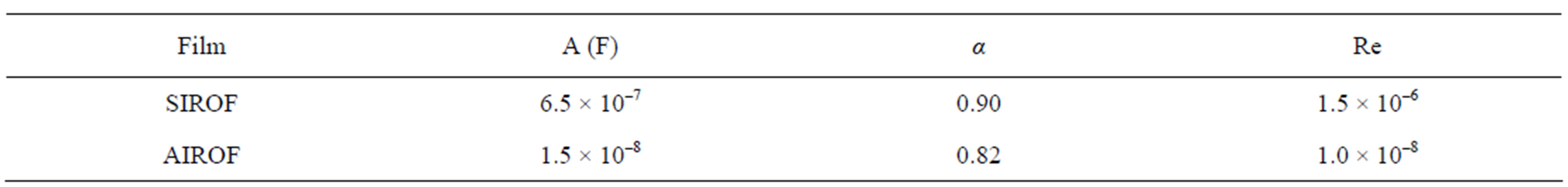
Table 1. Fitting results from the EIS model.
band width or measurement frequency. The Vrms for SIROF and AIROF was calculated to be 0.05 and 0.4 mV respectively, at 1 kHz bandwidth. The transmembrane action potentials amplitude is, typically in the range of several tens of millivolt [21]. Low impedance SIROF offers significantly low thermal noise and cut-off frequency compared to AIROF making SIROF a better recording and stimulating material.
The representative voltammograms of SIROF and AIROF, both having tip exposure of 50 μm  , is compared in Figure 8. The CV curve for SIROF has significantly larger internal area than for AIROF, indicating SIROF has higher CSC. However, SIROF does not exhibit the well defined reduction and oxidation peaks, which were observed for AIROF. The absence of oxidation-reduction peaks for SIROF is consistent with published work of other researcher [8]. Lack of peaks in SIROF CV may be attributed to lower ion transport rates within the film due to higher density of films. The median cathodal charge storage capacity (CCSC) of SIROF and AIROF coated UEAs for over 340 electrodes, was 44.3 ± 21.7 and 4.4 ± 3.1 mC/cm2, respectively. Researchers have reported CSC of AIROF with values from 20 - 35 mC/cm2 [11,22]. In each of these studies, the surface area and geometrical shape of the electrodes were different, and thickness of AIROF was not reported. CSC is a measure of charge available at near-equilibrium conditions. However, neural stimulation occurs at higher frequency, making CSC inadequate for stimulation material comparison. CV reveals the nature of current flow processes.
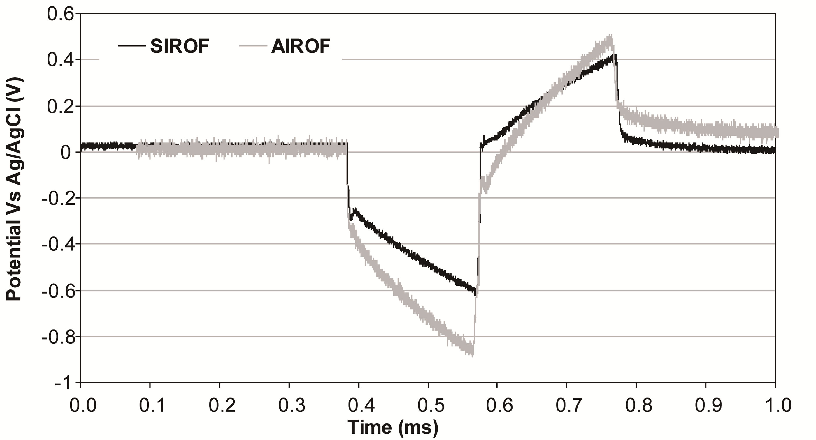
Figure 9 illustrates the potential transient of SIROF and AIROF coated UEA having similar tip exposure of 50 µm. Figure 9(a) illustrates the comparison of AIROF and SIROF coated UEA with 100 µA and 200 µs biphasic current pulse. Figures 9(b) and (c) illustrate the potential transient at different pulse width for AIROF and SIROF, respectively. Safe charge injection (Emc = –0.6 V) for unbiased SIROF and AIROF electrodes were calculated to be 2.0 and 1.0 mC/cm2, respectively, with 0.2 ms cathodic pulse at 50 Hz. These CIC values are consistent with published values for unbiased electrodes. Applying positive bias to SIROF electrode increases CIC in the range of 2 to 5 mC/cm2 [8,22], while AIROF electrodes increases in the range of 3 mC/cm2 and 4 mC/cm2 of charge [10,23]; though the neural damage threshold is roughly 1 mC/cm2 [24]. As shown in Figure 9(a), Vd is significantly lower in SIROF than AIROF. Hence, the power required to deliver a stimulation pulse will be smaller in SIROF which will prolong battery life, important factor for wireless stimulation.
CIC of SIROF is 5% of CSC, while for AIROF it is 20%. The film property like roughness, which is surface phenomena, and porosity (density), which is bulk phenomena, plays an important role in determining CIC. The
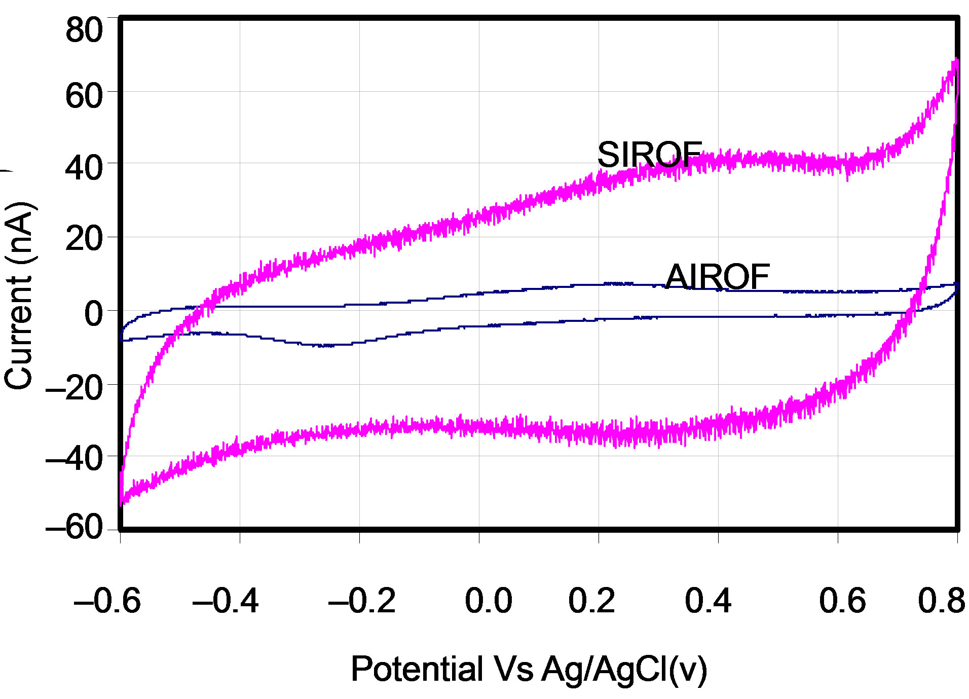
Figure 8. Representative CV curves for SIROF and AIROF coated electrodes of the UEA under similar conditions. The area and the shape of the SIROF CV are significantly different from that of AIROF CV.
 (a)
(a)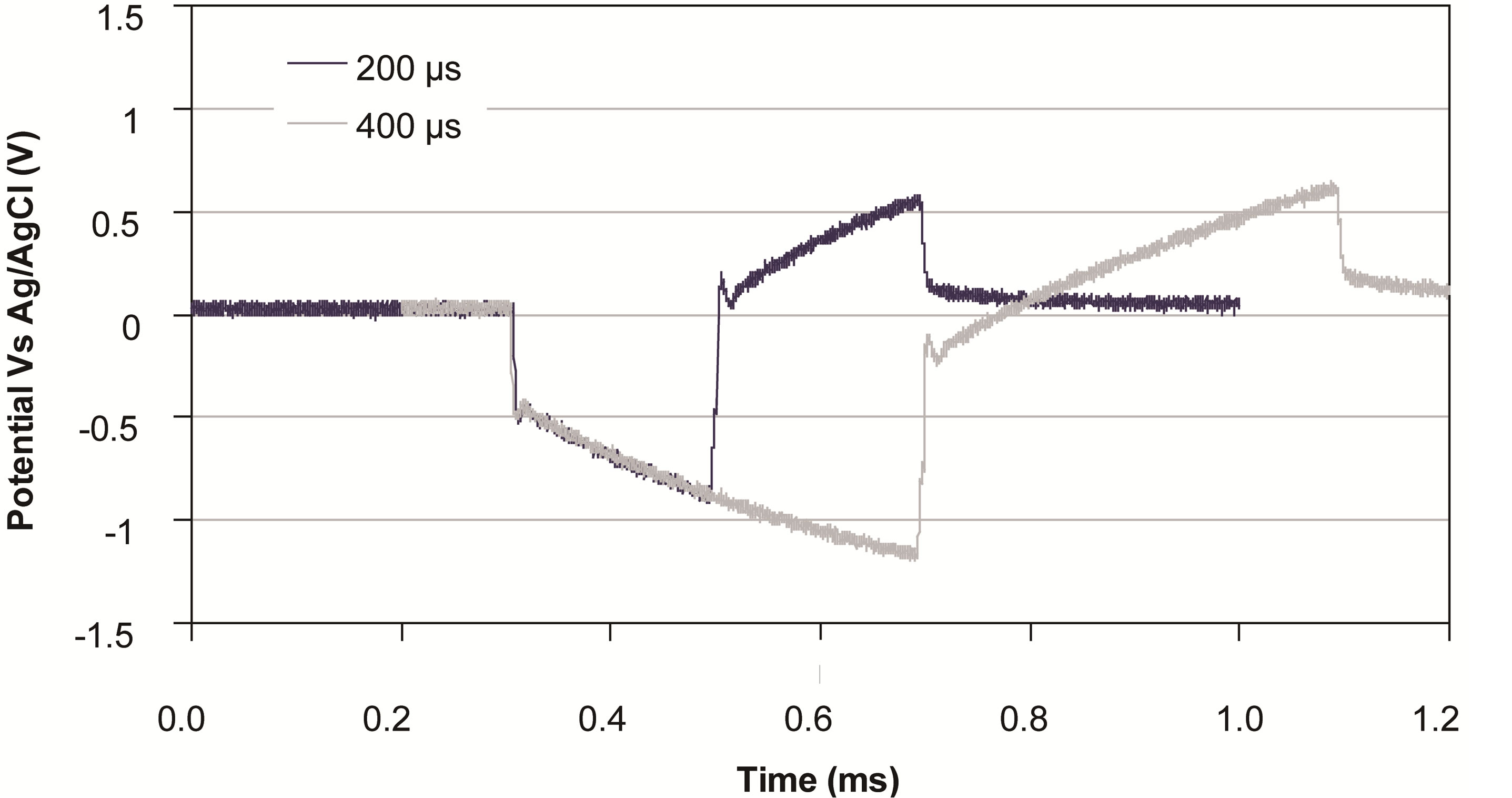 (b)
(b)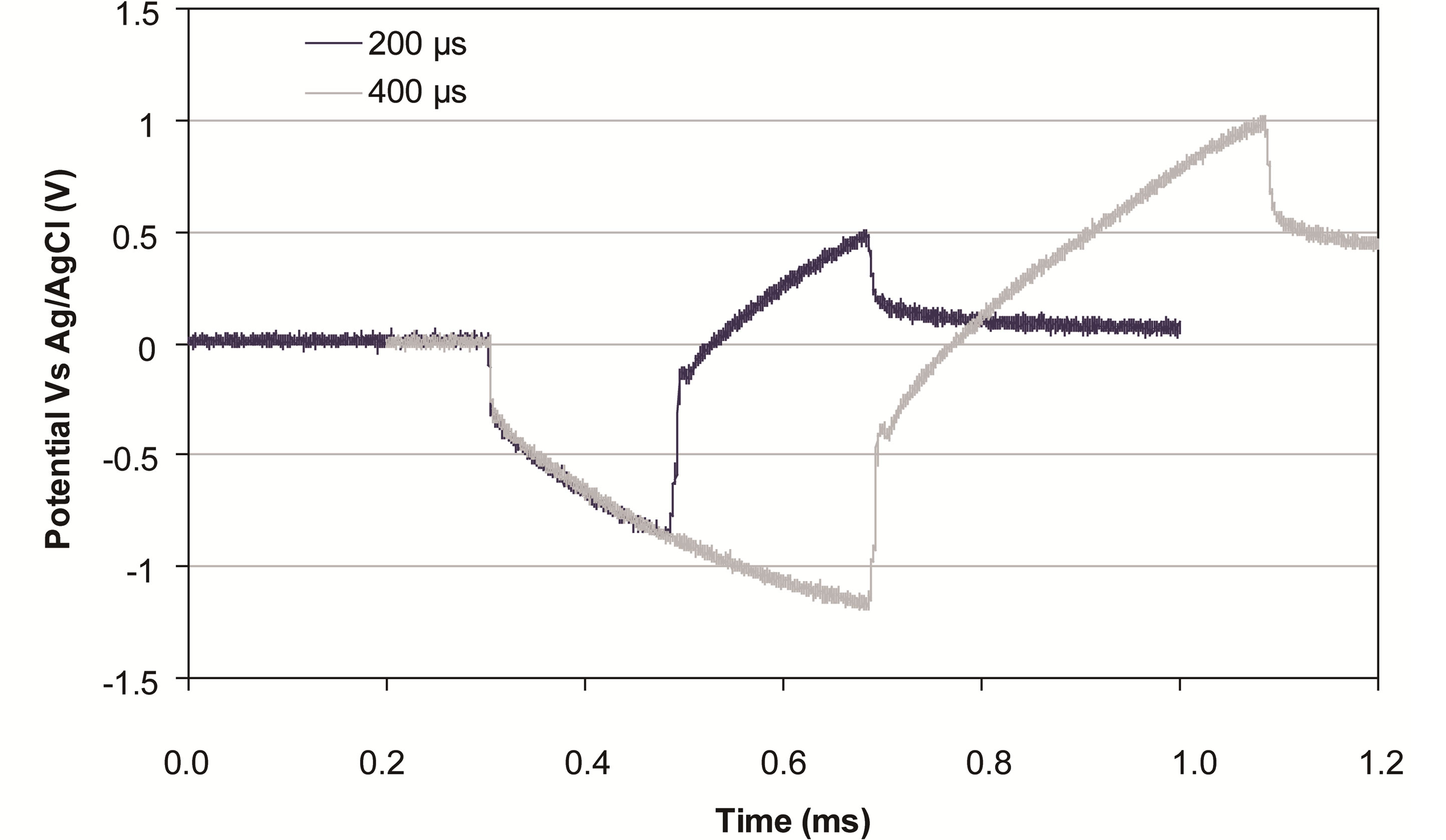 (c)
(c)
Figure 9. Voltage transient for SIROF and AIROF coated UEA in response to a biphasic current pulse. (a) Electrodes potential in response to a 100 µA and 200 µs current pulse. Potential transient of (b) AIROF in response to 100 µA and (c) SIROF in response to 200 µA pulses of varying duration.
density of SIROF and AIROF is 7 and 2 g/cm3, respectively [14]. AIROF was rougher than SIROF as deduced from the parameters (α) of CPE. CSC is measured at low frequency (in near-equilibrium condition), therefore charge carriers (electrons and ions in the electrolyte) have enough “time” to access more Ir ions in the IrOx films. Hence denser SIROF have superior CSC than AIROF. On the other hand, CIC is measured at higher frequency. Due to slow diffusion rate of ions in the electrolyte less number of Ir ions are accessed. Therefore, only small percentage of CSC is utilized in CIC. Nevertheless, unbiased SIROF has higher CIC than unbiased AIROF. Furthermore, though stability of SIROF under long term pulsing remains to be determined, preliminary studies suggest that SIROF is more tolerant of overpulsing than AIROF.
3.5. Electrode Impedance Relation to Tip Exposure
Figure 10 presents the UEA electrode impedance as a function of tip exposure. The SIROF electrodes were found to have significantly lower impedance than AIROF electrodes with tip exposures less than 100 μm. At 50 μm exposure, the SIROF and AIROF electrode impedance are 10 and 120 kOhm, respectively. The low impedance of SIROF coated electrodes is critical parameter for the efficiency of the arrays. For higher selectivity, a smaller tip exposure is required and for higher sensitivity lower impedance is required.
4. Conclusion
Iridium oxide remains the most promising stimulation
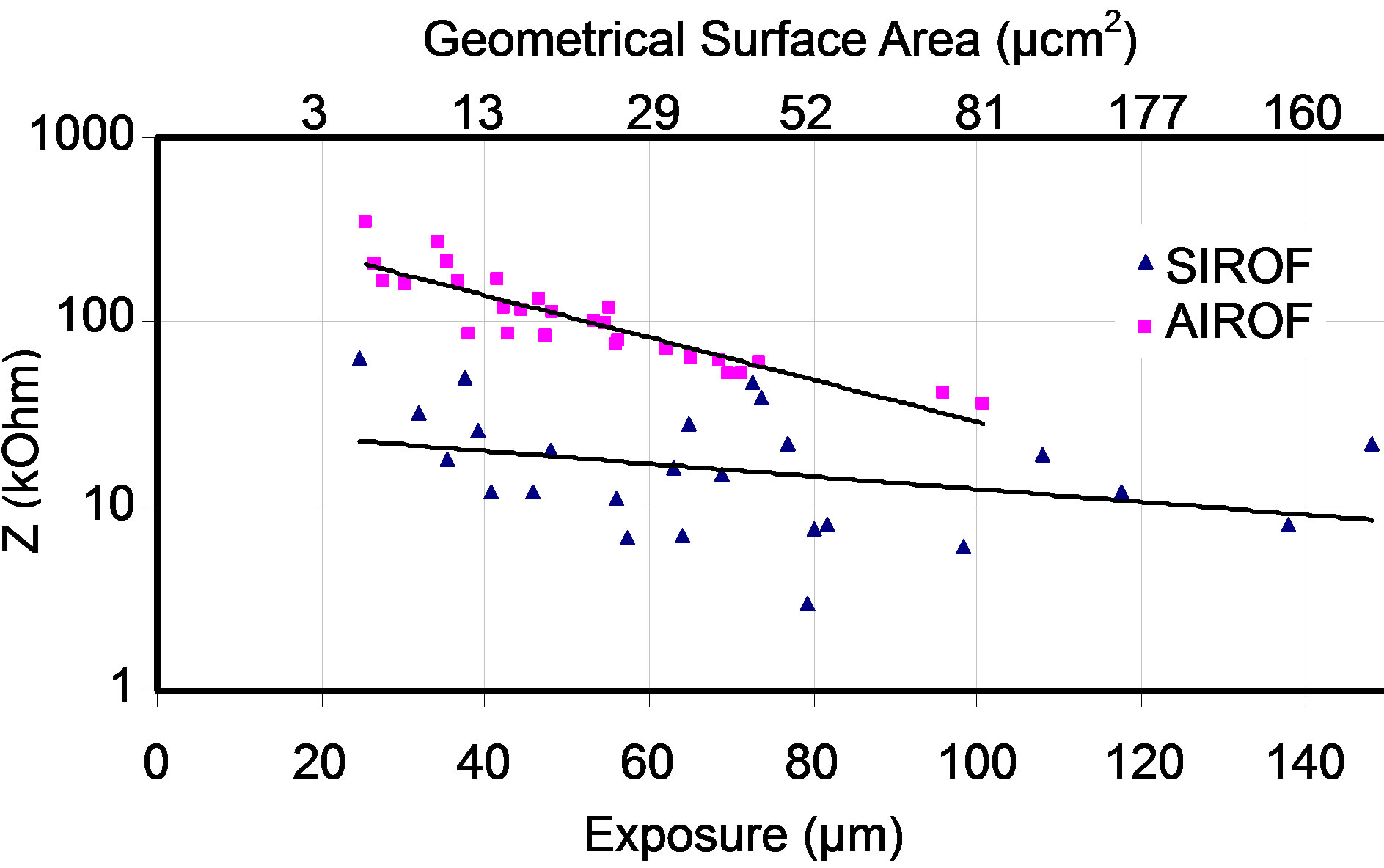
Figure 10. Electrode impedance is plotted as a function of tip exposure for SIROF and AIROF arrays. The length was measured by SEM and the solid line is the trend line with the equation.
and recording material. SIROF is well suited for deposition and patterning on non-planar substrates such as the UEA, however, an adhesion layer (Ti) is required. SIROF electrodes have higher CIC than AIROF electrodes. SIROF electrodes impedance (at 1 kHz) was ~10 times lower than that of AIROF electrodes for tip exposure of 50 μm. Although low impedance of the neural electrodes is not sufficient for good recording ability, but it is necessary requirement. SIROF will be of particular importance for wireless recording/stimulating arrays such as the integrated neural interfaces currently under development in University of Utah, which will not have wires that would be used for activation. SIROF is also more stable than AIROF when electrical pulses are applied to them [25]. It is clear that SIROF has superior electrochemical characteristics compared to that of AIROF. The higher charge capacity and lower impedance makes SIROF an attractive stimulation and recording electrode material and highly recommended for neuroprosthetic applications.
5. Acknowledgements
This project was funded by the National Institute of Neurological Disorders and Stroke (NINDS), National Institute of Health (NIH) grant number 1R43NS073162.
REFERENCES
- F. T. Hambrecht and J. Reswick, “Functional Electrical Stimulation: Application in Neural Prostheses,” Marcel Dekker, New York, 1977.
- R. A. Normann, “Technology Insight: Future Neuroprosthetic Therapies for Disorders of the Nervous System,” Nature Clinical Practice Neurology, Vol. 3, No. 8, 2007, pp. 444-452. doi:10.1038/ncpneuro0556
- J. D. Klein, S. L. Clauson and S. F. Cogan, “The Influence of Substrate Bias on the Morphology and Charge Capacity of RF-Sputtered Iridium Oxide Films,” Journal of Materials Research, Vol. 4, No. 6, 1989, pp. 1505- 1510. doi:10.1557/JMR.1989.1505
- J. D. Klein, S. L. Clauson and S. F. Cogan, “Morphology and Charge Capacity of Sputtered Iridium Oxide Films,” Journal of Vacuum Science & Technology A, Vol. 7, No. 5, 1989, pp. 3043-3047. doi:10.1116/1.576313
- J. A. Thornton, “Influence of Apparatus Geometry and Deposition Conditions on the Structure and Topography of Thick Sputtered Coatings,” Journal of Vacuum Science & Technology A, Vol. 11, No. 4, 1974, pp. 666-671. doi:10.1116/1.1312732
- H.-J. Cho, H. Horii, C. S. Hwang, J.-W. Kim, C. S. Kang, et al., “Preparation and Characterization of Iridium Oxide Thin Films Grown by DC Reactive Sputtering,” Journal of Applied Physics, Vol. 36, 1997, pp. 1722-1727. doi:10.1143/JJAP.36.1722
- C. U. Pinnow, I. Kasko, N. Nagel, S. Poppa, et al., “Influence of Deposition Conditions on Ir/IrO2 Oxygen Barrier Effectiveness,” Journal of Applied Physics, Vol. 91, No. 12, 2002, pp. 9591-9597.doi:10.1063/1.1471574
- E. Slavcheva, R. Vitushinsky, W. Mokwa and U. Schnakenberg, “Sputtered Iridium Oxide Films as Charge Injection Materials for Functional Electrostimulation,” Journal of the Electrochemical Society, Vol. 151, No. 7, 2004, pp. 226-237. doi:10.1149/1.1747881
- S. Negi, R. Bhandari, L. Rieth and F. Solzbacher, “Effect of Sputtering Pressure on Pulse-DC Sputtered Iridium Oxide Films,” Sensors and Actuators B: Chemical, Vol. 137, No. 1, 2009, pp. 370-378. doi:10.1016/j.snb.2008.11.015
- X. Beebe and T. L. Rose, “Charge Injection Limits of Activated Iridium Oxide Electrodes with 0.2 msec Pulses in Bicarbonate Buffered Saline,” IEEE Transactions on Biomedical Engineering, Vol. 35, No. 6, 1988, pp. 494- 495. doi:10.1109/10.2122
- L. S. Robblee, J. L. Lefko and S. B. Brummer, “Activated Iridium: An Electrode Suitable for Reversible Charge Injection in Saline Solution,” Journal of the Electrochemical Society, Vol. 130, No. 3, 1983, pp. 731-733. doi:10.1149/1.2119793
- P. F. Johnson and L. L. Hench, “An in Vitro Analysis of Metal Electrodes for Use in the Neural Environment,” Brain Behavior and Evolution, Vol. 14, No. 1-2, 1977, pp. 23-45. doi:10.1159/000124612
- R. Kotz, H. Neff and S. Stucki, “Anodic Iridium Oxide Films,” Journal of the Electrochemical Society, Vol. 131, 1984, pp. 72-77. doi:10.1149/1.2115548
- K. S. Kang and J. L. Shay, “Blue Sputtered Iridium Oxide Films (Blue SIROF’s),” Journal of the Electrochemical Society, Vol. 130, 1983, pp. 766-769. doi:10.1149/1.2119800
- J. D. E. McIntyre, W. F. Peck and S. Nakahara, “Oxidation State Changes and Structure of Electrochromic Iridium Oxide Films,” Journal of the Electrochemical Society, Vol. 127, 1980, pp. 1264-1268. doi:10.1149/1.2129868
- P. C. Liao, W. S. Ho, Y. S. Huang and K. K. Tiong, “Characterization of Sputtered Iridium Dioxide Thin Films,” Journal of Materials Research, Vol. 13, No. 5, 1998, pp. 1318-1326. doi:10.1557/JMR.1998.0187
- R. Bhandari, S. Negi and F. Solzbacher, “Wafer Scale Fabrication of Penetrating Neural Electrode Arrays,” Biomedical Microdevices, Vol. 12, No. 5, 2010, pp. 797-807. doi:10.1007/s10544-010-9434-1
- R. Bhandari, S. Negi, L. Rieth, R. A. Normann, et al., “A Wafer Scale Etching Technique for High Aspect Ratio Implantable MEMS Structures,” Sensors and Actuators A: Physical, Vol. 162, No. 1, 2010, pp. 130-136.
- S. Negi, R. Bhandari, L. Rieth and F. Solzbacher, “In Vitro Comparison of Sputtered Iridium Oxide and Platinum Coated Neural Implantable Microelectrode Arrays,” Biomedical Materials, Vol. 5, No. 1, 2010, Article ID: 015007.
- A. Norlin, J. Pan and C. Leygraf, “Investigation of Interfacial Capacitance of Pt, Ti and TiN Coated Electrodes by Electrochemical Impedance Spectroscopy,” Biomolecular Engineering, Vol. 19, No. 2-6, 2002, pp. 67-71. doi:10.1016/S1389-0344(02)00013-8
- B. He, “Neural Engineering: Interfacing Neural Tissue with Microsystems Bioelectric Engineering,” Kluwer Academic/Plenum Publishers, New York, 2005.
- S. F. Cogan, “Neural Stimulation and Recording Electrodes,” Annual Review of Biomedical Engineering, Vol. 10, 2008, pp. 275-309. doi:10.1146/annurev.bioeng.10.061807.160518
- S. F. Cogan, P. R. Troyk, J. Ehrlich and T. D. Plante, “In Vitro Comparison of the Charge Injection Limits of Activated Iridium Oxide (AIROF) and Platinum-Iridium Microelectrodes,” IEEE Transactions on Biomedical Engineering, Vol. 52, No. 9, 2005, pp. 1612-1614. doi:10.1109/TBME.2005.851503
- D. B. McCreery, W. F. Agnew, T. G. H. Yuen and L. Bullara, “Charge Density and Charge per Phase as Cofactors in Neural Injury Induced by Electrical Stimulation,” IEEE Transactions on Biomedical Engineering, Vol. 37, No. 10, 1990, pp. 996-1001. doi:10.1109/10.102812
- S. Negi, R. Bhandari, L. Rieth, R. V. Wagenen and F. Solzbacher, “Neural Electrode Degradation from Continuous Electrical Stimulation: Comparison of Sputtered and Activated Iridium Oxide,” Journal of Neuroscience Methods, Vol. 186, No. 1, 2010, pp. 8-17. doi:10.1016/j.jneumeth.2009.10.016
NOTES
*F. Solzbacher has a financial interest in the company Blackrock Microsystems, which develops and produces implantable neural interfaces, and electrophysiology equipments and software.
#Corresponding author.