Modern Mechanical Engineering
Vol. 3 No. 2 (2013) , Article ID: 31654 , 10 pages DOI:10.4236/mme.2013.32015
Investigation of a Pressure Sensor with Temperature Compensation Using Two Concentric Wheatstone-Bridge Circuits
1Department of Mechanical and Automation Engineering, National Kaohsiung First University of Science and Technology, Taiwan
2Department of Product Design, Shu-Te University, Taiwan
3Department of Mechanical and Automation Engineering, National Kaohsiung First University of Science and Technology, Taiwan
Email: hungcc16@stu.edu.tw
Copyright © 2013 Chi-Chang Hsieh et al. This is an open access article distributed under the Creative Commons Attribution License, which permits unrestricted use, distribution, and reproduction in any medium, provided the original work is properly cited.
Received March 4, 2013; revised April 19, 2013; accepted April 30, 2013
Keywords: Pressure Sensor; Temperature Compensation; Wheatstone-Bridge Circuit; MEMS
ABSTRACT
This study presents a silicon-based pressure sensor with temperature compensation. The eight piezoresistors were designed on the polycrystalline silicon membrane and constructed by two concentric Wheatstone-bridge circuits to perform two sets of sensors. The sensor in the central circuit measures the membrane deflection caused by the combined effects of pressure and temperature, while the outer one measures only the deflection caused by the working temperature. From this arrangement, it is reliable and accurate to measure the pressure by comparing the output signals from the two concentric Wheatstone-bridge circuits. The optimal positions of the eight piezoresistors were simulated by simulation software ANSYS. The investigated pressure sensor was fabricated by the micro electro-mechanical systems (MEMS) techniques. The measuring performance and an indication of the conventional single Wheatstone-bridge pressure sensor is easily affected under variation of different working temperature and causes a maximum absolute error up to 45.5%, while the double Wheatstone-bridge pressure sensor is able to compensate the error, and reduces it down to 1.13%. The results in this paper demonstrate an effective temperature compensation performance, and have a great performance and stability in the pressure measuring system as well.
1. Introduction
Pressure sensors have been extensively applied in the automobile industries, environmental monitoring systems, process controls and biomedical fields [1-4]. The pressure sensor was traditionally manufactured by large-scale mechanical devices, while recently the micro-electromechanical systems (MEMS) technologies have the advances and great improvements to fabricate highly-sophisticated micro-sensors with excellent repeatability characteristics and ultra-low-pressure detection capabilities [5-7]. In such devices, the pressure is generally measured by piezoelectric thin films [8,9] or the form of capacitance structures [10]. Since the capacitive-type pressure sensors have better sensitivity to the influences of the parasitic capacitance, this pressure sensors do not interfere with the test results of pressure by the outer temperature. By contrast, the sensitivity, linearity and repeatability characteristics of the piezoresistive-type pressure sensors have been greatly improved, and can be easily manufactured by mass production using standard MEMS-based techniques to reduce the cost [11,12]. Most of piezoresistive pressure sensors are easy to produce the error or deformation for test result of pressure when the outer temperature yields variations. In the conventional piezoresistive pressure sensors, the sensing element has four diffused or ion-implanted strain gauges which compose a single Wheatstone-bridge circuit on a thin silicon membrane [13]. Such devices have the drawback of zeropressure offset error due to the temperature [14]. It was shown that the zero-pressure offset error in the single Wheatstone-bridge piezoresistor was primarily caused by the thermal residual stresses due to different thermal expansion coefficients of the monocrystalline silicon substrate and the polycrystalline silicon membrane [15,16]. In Reference [15], the dual bridge pressure sensor only considers the different pressure variables will lead to what influences for the test result of the pressure sensor. However, the different pressure and temperature variables should be included in the measurement of the pressure sensor.
The purpose of this paper is to present a piezoresistive pressure sensor which composed by two concentric Wheatstone-bridge circuits on a polycrystalline silicon membrane, shown in Figure 1. This piezoresistive pressure sensor has accurately compensation of temperature, high-sensitivity, and high-reliability characteristics. The proposed pressure sensor was fabricated by conventional MEMS-based techniques, including low-pressure chemical vapor deposition (LPCVD), light-boron and heavy-boron ion implantation, dry etching, electrochemical etch-stop processing, and anodic bonding. In this investigation, the eight piezoresistors were designed on the polycrystalline silicon membrane, see Figure 1, and this design is to find out the best arrangement of the two central and the outer Wheatstone-bridge circuits to compensate the errors. For this reason, this study is to combine the pressure sensor circuit (inner piezoresistors) and temperature compensation circuit (outer piezoresistors) on the same sensor. It can not only enhance the performance, but also shrink the volume of the pressure sensor system.
The four piezoresistors of the Wheatstone-bridge circuit in the central region on the membrane measure the membrane deflection caused by the combined effects of the pressure and temperature, while the four outer ones measure only the deflection caused by the thermal load. A reliable indication of the pressure measurement can therefore be obtained by combining the output signals of the two Wheatstone-bridge circuits under different temperature surroundings. Here, the stress distributions caused by the working temperature and pressure respecttively on the membrane was simulated by finite element analysis (FEA) method and ANSYS software tool in order to establish the optimal locations of the eight piezoresistors in each Wheatstone-bridge circuits. The experi-
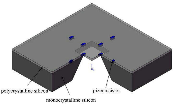
Figure 1. Illustration of the two concentric Wheatstonebridge circuits on the polycrystalline silicon membrane.
ment conditions of the introduced pressure sensor are under the pressures ranging from zero to 150 psi and the temperatures ranging from −10˚C to 75˚C.
2. Numerical Simulation and Analysis
In the practical applications of pressure sensors, the membrane deformations are caused by both the working temperature and pressure. The variations of temperature will affect the measuring result of pressure. The phenomena call thermal stress when the variations of pressure lead to the membrane deformations. Therefore, the thermal stress is a major pressure course for the membrane. And, the different materials have different values of thermal expansions and contractions that will bring about different thermal stress. Similarly, different locations of the piezoresistors will lead to different result of membrane deformations. As a result, by using the simulation to analysis the influence of pressure is absolutely to do when establish the model in the initial phase. Here, this study used the FEA as the simulation and analysis method. And, by applying the ANSYS software as the simulation and analysis tool to obtain the maximum pressure distribution, and thus, the optimal locations of the piezoresistors on the membrane will be got.
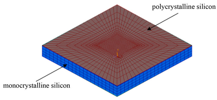
Figures 2(a) and (b) illustrate the top and bottom views of the FEA model respectively. The settings and definitions of the materials are basically monocrystalline and polycrystalline silicon. Recently, the integrated circuit trends to have more and more complex with multifunctions but smaller and smaller in size. It needs much more exact calculation and designation for electrical characteristics. Poor design and process-induced mechanical stress effect will cause serious problem during fabrication stages, especially for the packaging process in the front-end process, which make more variation to electrical characteristics and affect the quality and performance of the device in the end. Mechanical stress induced unstable and variation of electrical characteristics is one of the major factors to affect the entire performance of a device seriously. And, the different type of silicon has the different direction of etch in the process of fabrication. The different direction of etch will affect the electrical characteristics of sensor. Therefore, in this study, the monocrystalline silicon is design as the substrate, where the polycrystalline silicon is the membrane of the pressure sensor. The polycrystalline silicon membrane will deform when the pressure is loaded, and the deformation analysis due to the thermal stresses can be calculated by different thermal expansion coefficients of the monocrystalline and polycrystalline silicon materials. The properties of the materials are shown in Table 1.
Considering the boundary conditions in the ANSYS software, the displacement of each node along the X, Y, Z axes at the bottom of the substrate respectively are set
 (a)
(a)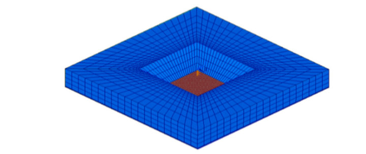 (a)
(a)
Figure 2. The (a) top view, and (b) bottom view of the ANSYS FEA model.
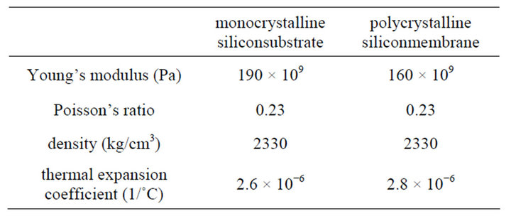
Table 1. Material properties of the monocrystalline substrate and the polysilicon membrane.
to be zero. The types of the loadings are considered as: pressure loadings and temperature loadings. The loading conditions are divided into three parts: applying temperature without pressure; applying pressure at room temperature (25˚C); and applying both pressure and temperature loadings. Under the above loading conditions, the effects and influences about the pressure and temperature to the membrane deformations can be analyzed. The values of the loading conditions are ranging from zero to 150 psi, and −10˚C to 75˚C for pressure and temperature respectively. Since the stress distributions caused by simply pressure loading, simply temperature loading, or both pressure and temperature loadings, the pressure and temperature distributions on the membrane of the pressure sensor can be known after the simulation. Furthermore, the best locations of the four inner piezoresistors can be obtained based on the maximum stress distribution to perform an effective output measurement indication.
3. Fabrication Process and Measurement
In this study, the fabrication of the proposed double Wheatstone-bridge pressure sensor is in comparison with the conventional single Wheatstone-bridge pressure sensor. Both the dimensions are  μm in length, width, and height respectively.
3.1. Fabrication of the MEMS-Based Pressure Sensors
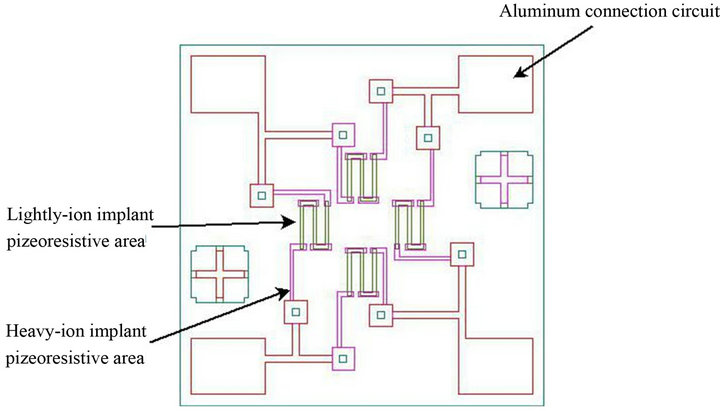
In the fabrication process, the two types of sensors were patterned using the mask designs shown in Figures 3(a) and (b) respectively. Note that the patterning process was performed using cheaper film-photo masks with 30 μm line width and only two quartz masks with 1 μm line width respectively. As a result, it was found that the application of combining the two types of masks above reduced nearly 40% of the fabricating cost.
Figure 4 illustrates a schematic overview of the fabrication processes of the two types of pressure sensors, and the only difference is the choices of the mask patterns. In the beginning, a thin (20 μm) layer of polycrystalline silicon was deposit by the LPCVD technique on the surface of monocrystalline silicon substrate. The substrate was then located in the oxidation furnace at temperature 1092˚C and pressure 1 Pa for 30 hours to form a thin (800 Å) silicon oxide layers on the top and bottom surfaces of it shown in Figure 4(a). The substrate was then patterned using a photolithography technique, and immersed in a Buffered Oxide Etch (BOE) solution to remove the silicon oxide layer from the bottom surface. Partly of the silicon oxide layer from the top surface was also removed at the same time in order to create the designed basic outline of the piezoresistor structures shown in Figure 4(b). An ion-implantation method was then utilized to implant the polycrystalline silicon layer with boron to create the piezoresistor structures. In order to establish a resistance gradient within the structure, the light-ion implantation process was initially performed with 3.2 × 10¹⁴ atom/cm3 boron implant intensity to create a thin and high-resistance boron layer shown in Figure 4(c). After this procedure, the heavy-ion implantation process was performed with 1.5 × 10¹⁶ atom/cm3 boron implant intensity to create a thicker and low-resistance layer shown in Figure 4(d). Note that in both cases of the plating processes are performed by 80 KeV implantation energy. In the following procedure, the LPVCD technique was utilized to deposit the silicon nitride layers with a thickness of 1400 Å on the top and bottom surfaces of the substrate shown in Figure 4(e). A reactive ion etching (RIE) process was then performed to remove the silicon nitride layer from the top surface shown in Figure 4(f). After this, an aluminum layer with a thickness of 900 Å was sputtered on the top surface, patterned lithographically using AZ5214N photoresist, and etched at a temperature of 65˚C in H3PO4 acid to create the electrical Wheatstone-bridge circuits shown in
 (a)
(a)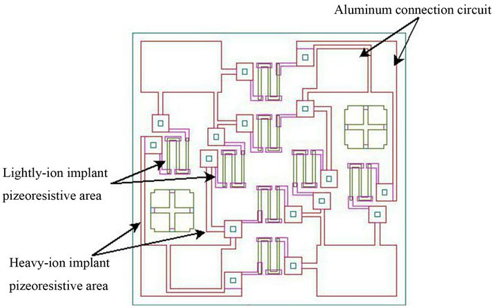 (b)
(b)
Figure 3. Mask designs of (a) the single Wheatstone-bridge, and (b) the double Wheatstone-bridge pressure sensors.
Figure 2. The silicon nitridelayer on the bottom surface of the substrate was then removed using a RIE process in order to produce an etching mask shown Figure 4(g), and the substrate was etched by KOH chemical composition to create a cavity shown in Figure 4(h). Eventually, the remaining silicon nitride layer was removed from the bottom surface of the substrate by an etching process shown in Figure 4(i), and the substrate was finally fused with 7740 glass by an anodic bonding technique at 470˚C temperature shown in Figure 4(j).
The substrate cavity was etched by an electrochemical etch-stop process to accurately control the etching depth, and not to destroy the polycrystalline silicon membrane. The criterion of etching stop depends on the etching depth. In this study, a small current was initially detected after 150 minutes etching, and a large amount of silicon substrate was removed. It was observed that the current increased radically after 250 minutes etching, and this indicates that the etching process was completed and stopped, and the polycrystalline silicon membrane was not destroyed yet. Figure 5 illustrates the variations of currents with time in the electrochemical etch-stop process. Figure 6 shows an optical microscope image of the etched cavity, and Figure 7 shows a cross-sectional scanning electron microscope (SEM) image of the pressure sensor bonded with 7740 glass.
3.2. Packaging of the Pressure Sensor
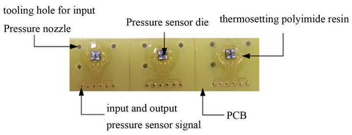
After the following fabrication process described in the above section, a total number of 1600 pressure sensor dies were manufactured. The individual pressure sensor die was then ready to be separated using a diamond cutter and assembled to a printed circuit board (PCB) by epoxy glue at temperature 80˚C for 25 minutes shown in Figure 8(a). Thereafter, the gold wires were bonded between the sensor die and the PCB, and then packaged by a thermo-setting polyimide resin at a temperature 100˚C for 30 minutes. Finally, an input pressure nozzle and an O-ring were assembled shown in Figure 8(b).
3.3. Measurement of the Pressure Sensor
Figure 97-2700704o types of the pressure sensors were tested at temperatures ranging from −10˚C to 75˚C and pressures ranging from zero to
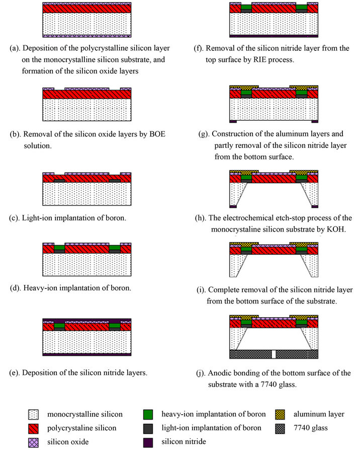
Figure 4. Overview of the pressure sensor fabrication process.
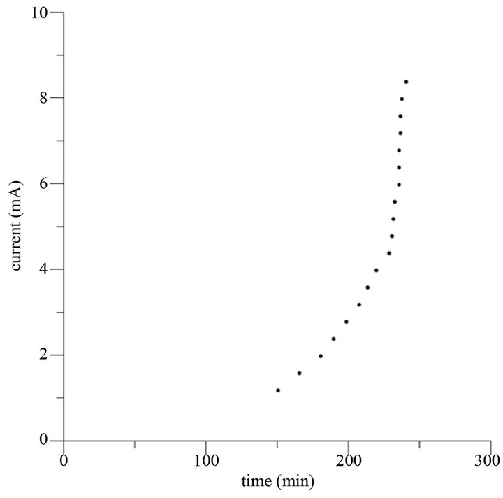
Figure 5.The variations of currents with time in the electrochemical etch-stop process.
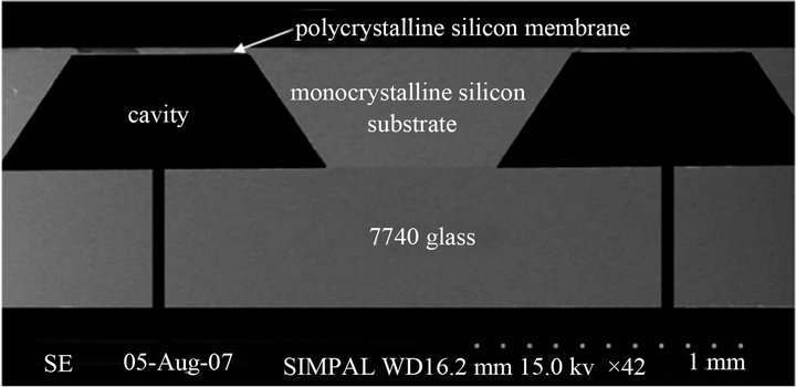
Figure 6. An optical microscope image of the etched cavity.
150 psi in the GH800 GIANT FORCE chamber, and the pressure was supplied by a high pressure gas cylinder which was controlled by the DRUCK DPI515 system. The input voltage was supplied by Agilent-E3633A DC power supply with 50V maximum output voltage and 4A current. The output signal of the pressure sensors was measured by GW-DIGITAL MULTIMETER (GDM- 8055) with a minimum 1 μV measuring accuracy.
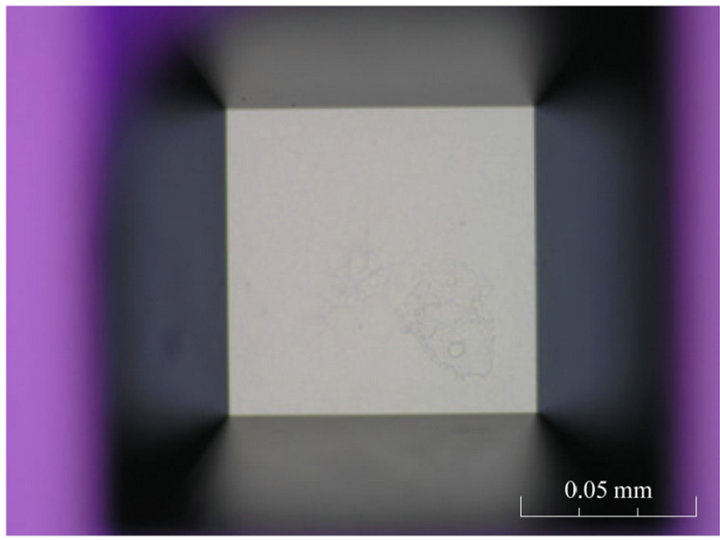
Figure 7. A cross-sectional SEM image of the pressure sensor bonded with a 7740 glass.
 (a)
(a)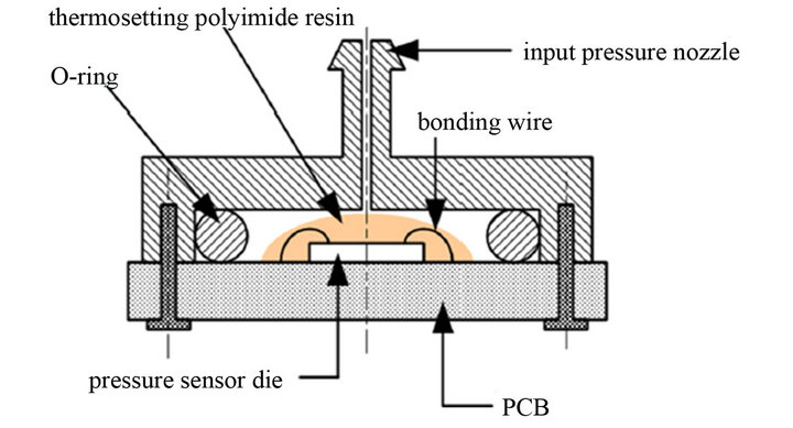 (a)
(a)
Figure 8. (a) Assembly of the pressure sensor dies to a PCB, and (b) A cross-sectional diagram of the feedback pressure sensor.
4. Results and Discussions
4.1. Design and FEA Results
Figures 10 and 11 illustrate the simulation results of the proposed pressure sensor, and show the equivalent von Mises stress distributions calculated by ANSYS software. Since the temperature has an obvious effect to the membrane and lead to it yields the deformation, the membrane deformed locations can be used to set the four outer piezoresistors in order to perform the temperature compensation. Figure 10 illustrates the simulation resultunder 75˚C thermal load without pressure in order to estimate the locations of estimate the four outer piezoresistors, and the temperature should take into consideration if the working temperature is above the 25˚C room temperature. When the pressure sensor has been pressured, the edge of middle of the membrane will be produced maximum stress. The location with the edge of middle of the membrane can be used to set the four inner piezoresistors. Figure 11 shows the equivalent von Mises stress distribution of the pressure sensor under the combination of 75˚C thermal load and 150 psi pressure load and it estimates the locations of the four inner piezoresistors. Therefore, this study in order to find out the optimal designing location of the two concentric Wheatstone-bridge circuits, it is necessary to know the maximum stress distributions which caused by the thermal and pressure loads individually, shown in the Figures 10 and 11. As a result, the centric Wheatstone-bridge circuit was selected to design in the location where the maximum von Mises stress appeared due to the pressure load. And the outer one is located where the maximum von Mises stress appeared due to the thermal load.
4.2. Analysis of the Output Voltage Affected by Temperature and Pressure
In the following subsections demonstrate that the temperature has a considerable effect to the output voltage in the conventional single Wheatstone-bridge pressure sensor. Nevertheless, the proposed pressure sensor is able to compensate the error affected by the working temperature using the double Wheatstone-bridge circuits design.
4.2.1. The Relation of the Output Voltage to the Pressure Load under Fixed Temperature
The experiment input voltage was set to be 5 V for the single Wheatstone-bridge pressure sensor at 25˚C room temperature, and the pressure values were set to be zero psi, 50 psi, 100 psi, and 150 psi as the input parameters respectively. Therefore, the 0.358 V, 0.270 V, 0.191 V, and 0.110 V output voltages were measured respectively. The diagram of the measured output voltages  to the input pressures (P) are shown in Figure 12, and their relation can be obtained as an idealized equation below:
 (1)
(1)
The idealized output voltage at 25 psi, 75 psi, and 125 psi respectively can then be calculated in advance from Equation (1) shown in Figure 13, and the 0.32%, 0.66%, and 2.63% absolute error in comparison with the measured values were analyzed respectively. It demonstrated that the pressure sensor with a single Wheatstone-bridge circuit has its accuracy and approximately linear output properties at room temperature under zero to 150 psi input pressure load.
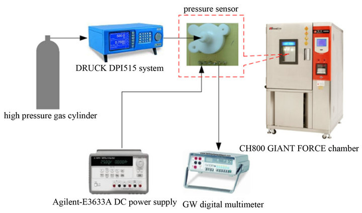
Figure 9. A schematic illustration of the layouts and equipments for the measurement.
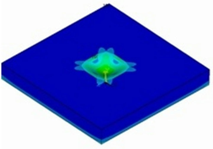
Figure 10. Results of the ANSYS FEA simulationunder 75˚C thermal load without pressure.
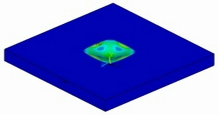
Figure 11. Results of the ANSYS FEA simulation under the combination of 75˚C thermal.
4.2.2. Analysis of the Output Voltage to the Input Pressure under Different Temperature
The output voltages of the single Wheatstone-bridge pressure sensor were then experimented and measured under different temperature circumstances. It was found in Figure 14 that the output voltage varied from 0.335V to 0.390 V under zero pressure setting with a temperature variation from −10˚C to 75˚C. The values of the output voltage without pressure loadings are the so-called zeropressure offset errors. These values are very critical and will lead to further errors. Figure 14 illustrates that the zero-pressure offset errors under different temperature conditions exist a maximum 8.2% absolute error in comparison with the standard output voltage at 25˚C room temperature. Furthermore, Figure 14 also illustrates the output voltages of the single Wheatstone-bridge pressure sensor varied from 0.060 V to 0.178 V at 150 psi pressure loading under different temperature conditions, and there exists a maximum 45.5% absolute error in comparison with the standard output voltage at 25˚C room temperature. The experiment proved that the accuracy of the single Wheatstone-bridge pressure sensor is easily affected by the surrounding temperature that leads to zeropressure offset errors.
4.3. Figures and Tables
According to the above section, the single Wheatstonebridge pressure sensor is easily to produce the zeropressure offset errors by the different surrounding temperature. The proposed pressure sensor will improve this disadvantage. From the measurement of experiments, it was found that the zero-pressure offset errors can be reduced by means of the proposed design under different working temperature shown in Figure 15. The values of the measured output voltage varied from 0.0766 V to 0.0768 V under zero pressure setting with a temperature variation from −10˚C to 75˚C. The zero-pressure offset error of the proposed design has only a maximum 0.06% absolute error in comparison with the standard output voltage at 25˚C room temperature, and has a great compensation improvement up to 99.94% caused by the surrounding temperatures. Furthermore, Figure 15 alsoillustrates the output voltages varied from 0.0745 V to 0.0747 V at 150 psi pressure loading under different temperature conditions, and there only exists a maximum 1.13% absolute error in comparison with the standard output voltage at 25˚C room temperature. It was found that the error will not increase with the increasing pres-
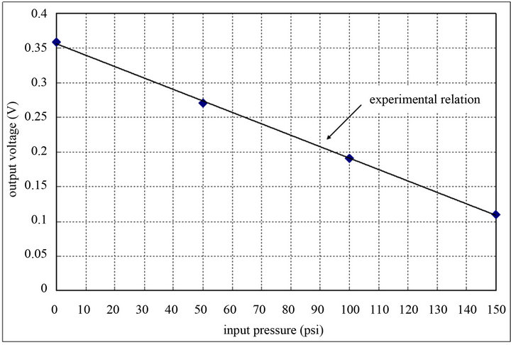
Figure 12. The relation between the measured output voltages and the input pressures under 0 psi, 50 psi, 100 psi, and 150 psi pressure loads respectively.
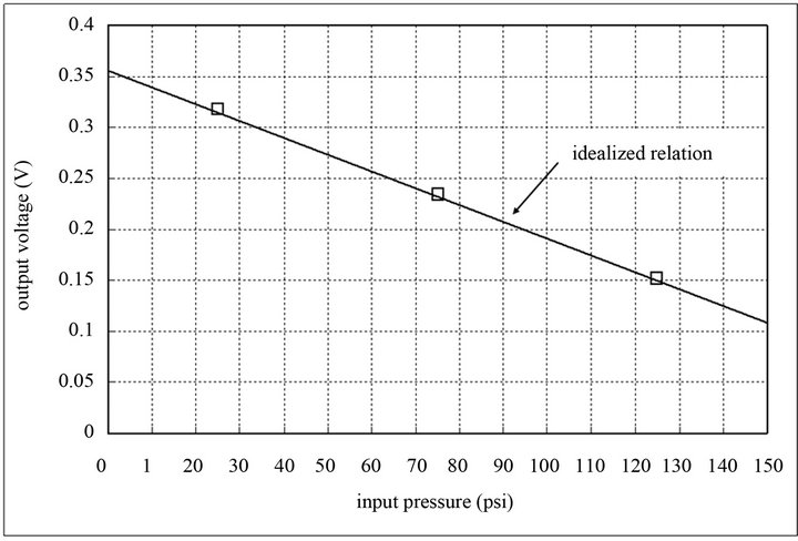
Figure 13. The relation between the measured output voltages and the input pressures under 25 psi, 75 psi, and 125 psi pressure loads respectively.
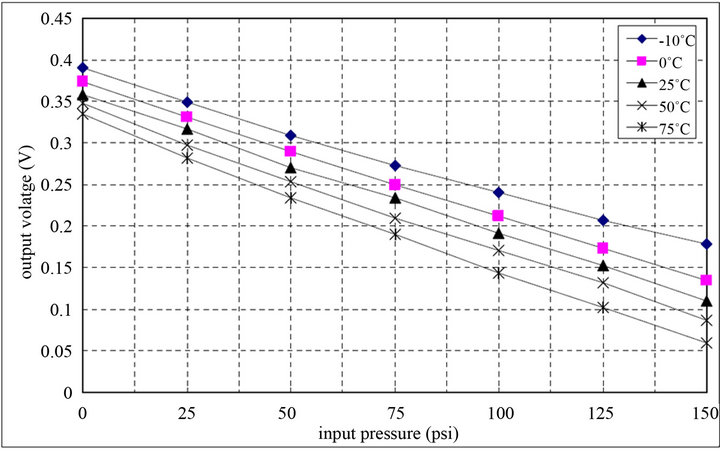
Figure 14. The relation between the measured output voltages and the input pressures of the single Wheatstone-bridge pressure sensor.
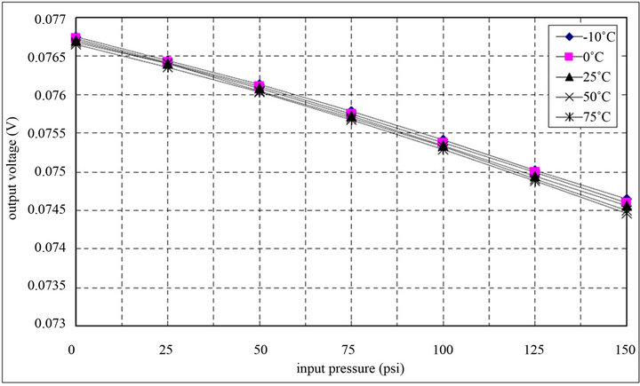
Figure 15. The relation between the measured output voltages and the input pressures of the proposed double Wheatstonebridge pressure sensor.
sure loading. The proposed pressure sensor is better than the single Wheatstone-bridge pressure sensor when compared the results between the Figures 14 and 15. Consequently, it has been proved that the proposed double Wheatstone-bridge pressure sensor has its accuracy and stability for the application to the pressure measuring system under temperatures ranging from −10˚C to 75˚C.
5. Conclusion
The double Wheatstone-bridge pressure sensor with temperature compensation that proposed in this paper is fabricated by MEMS techniques. And, it is based on FEA method and ANSYS tool to simulate and analyze the optimal locations of the inner and outer piezoresistors in the membrane. The proposed pressure sensor with temperature compensation has been proved to have a better accuracy and stability in comparison with the conventional single Wheatstone-bridge pressure sensor. And, it enables to enhance the test result of pressure effectively and exactly when the pressure sensor faces the bad surrounding temperatures. The fabrication process proposed in this study can reduce nearly 40% of the manufacturing cost by using only two quartz masks. The maximum zero-pressure offset error was found to be only 0.06% in comparison with the standard output voltage at 25˚C room temperature, and had a great improvement of temperature compensation up to 99.94%. Furthermore, maximum absolute error of the output voltage in comparison with the standard one at room temperature reduces down to 1.13%. As a result, the proposed pressure sensor with temperature compensation can be applied to the pressure measuring systems, high-tech industry, or vehicle safety systems, and it will benefit to increase the production yield rates for these industries.
6. Acknowledgements
This research was partly sponsored by the National Science Council of Taiwan under contracts NSC 98-2622- E-327-005-CC3 and NSC 98-2221-E-132-004.
REFERENCES
- S. A. Wright, H. Z. Harvey and Y. B. Gianchandani, “A Microdischarge-Based Deflecting-Cathode Pressure Sensor in a Ceramic Package,” Journal of Microelectromechanical Systems, Vol. 22, No. 1, 2013, pp. 80-86
- A. L. Kang, W. B. Wang, Y. Q. Liu and T. Han, “A Wireless Pressure Sensor Based On Surface Transverse Wave,” IEEE Conference Publications, Shenzhen, 9-11 December 2011, pp. 231-235.
- Y. Nam and J. W. Park, “Child Activity Recognition Based on Cooperative Fusion Model of a Triaxial Accelerometer and a Barometric Pressure Sensor,” IEEE Journal of Biomedical and Health Informatics, Vol. 17, No. 2, 2013, pp. 420-426.
- X. Meng, K. D. Browne, S. M. Huang, C. Mietus, D. K. Cullen, M. R. Tofighi and A. Rosen, “Dynamic Evaluation of a Digital Wireless Intracranial Pressure Sensor for the Assessment of Traumatic Brain Injury in a Swine Model,” IEEE Transactions on Microwave Theory and Techniques, Vol. 61, No. 1, 2013, pp. 316-325. doi:10.1109/TMTT.2012.2224361
- M. M. Sisto, S. García-Blanco, L. L. Noc, B. Tremblay, Y. Desroches, J.-S. Caron, F. Provencal and F. Picard, “Pressure Sensing in Vacuum Hermetic Micropackaging in MOEMS-MEMS,” Journal of Micro/Nanolithography, MEMS, and MOEMS, Vol. 9, No. 4, 2012, Article ID: 041109.
- L. Sujatha, V. S. Kale and E. Bhattacharya, “Critical Study of High-Sensitivity Pressure Sensors with Silicon/Porous Silicon Composite Membranes,” Journal of Micro/ Nanolithography, MEMS, and MOEMS, Vol. 8, No. 3, 2009, Article ID: 033070.
- Z. Wen, Z. Wen, G. Chen and S. Xu, “Fabrication of a Novel Vacuum Microelectronic Pressure Sensor,” Journal of Micro/Nanolithography, MEMS, and MOEMS, Vol. 3, No. 4, 2004, pp. 574-578.
- P. Gonzalez, B. Guo, M. Rakowski, K. D. Meyer and A. Witvrouw, “CMOS Compatible Polycrystalline SiliconGermanium Based Pressure Sensors,” Sensors and Actuators A: Physical, Vol. 188, 2012, pp. 9-18. doi:10.1016/j.sna.2011.12.018
- J. T. Huang and S. C. Cheng, “Study of Injection Molding Pressure Sensor with Low Cost and Small Probe,” Sensors and Actuators A: Physical, Vol. 101, No. 3, 2002, pp. 269-274. doi:10.1016/S0924-4247(02)00217-0
- G. Chitnis, T. Maleki, B. Samuels, L. B. Cantor and B. Ziaie, “A Minimally Invasive Implantable Wireless Pressure Sensor for Continuous IOP Monitoring,” IEEE Transactions on Biomedical Engineering, Vol. 60, No. 1, 2013, pp. 250-256. doi:10.1109/TBME.2012.2205248
- L. Kaabi, A. Kaabi, J. Sakly and M. F. Abdel Malek, “Modeling and Analysis of MEMS Sensor Based on Piezoresistive Effects,” Materials Science and Engineering: C, Vol. 27, No. 4, 2007, pp. 691-694.
- Z. Dibi, A. Boukabache and P. Pons, “Effect of the Membrane Flatness Defect on the Offset Voltage of a Silicon Piezoresistive Pressure Sensor,” ICECS Proceedings of the 10th IEEE International Conference, United Arab Emirates, 14-17 December 2003, pp. 902-905.
- J. Wang, X. Xia and X. Li, “Monolithic Integration of Pressure plus Acceleration Composite TPMS Sensors with a Single-Sided Micromachining Technology,” Journal of Microelectromechanical Systems, Vol. 21, No. 2, 2012, pp. 284-293. doi:10.1109/JMEMS.2011.2178117
- M. J. Hu, B. C. Sang and H. L. Jong, “Design of Smart Piezoresistive Pressure Sensor, Science and Technology,” The 5th Korea-Russia International Symposiumon Science and Technology, Tomsk, 26 June-31 July 2001, pp. 202-205.
- C. Pedersen, S. T. Jespersen, J. P. Krog, C. Christensen and E. V. Thomsen, “Combined Differential and Static Pressure Sensor Based on a Double-Bridged Structure,” Sensors Journal for IEEE, Vol. 5, No. 3, 2005, pp. 446-454. doi:10.1109/JSEN.2005.845199
- T. L. Young, D. S. Hee, K. Akihisa, Y. Tetsuhiro, M. Yoshinori, I. Makoto and N. Tetsuro, “Compensation Method of Offset and Its Temperature Drift in Silicon Piezoresistive Pressure Sensor Using Double WheatstoneBridge Configuration,” 8th International Conference on Solid-State Sensors and Actuators, Stockholm, 25-29 June 1995, pp. 570-573.